Panasonic EvalBoard PAN4555 User manual

CLASSIFICATION
Einstufung PRELIMINARY No.
DS-Eval4555-2400
REV.
01
SUBJECT
Thema
EvalBoard PAN4555
PAGE
Seite
1 of 16
CUSTOMER’S CODE
EvalPAN4555
PANASONIC’S CODE
DATE
Datum
30.03.2007
European Technology Center
Panasonic Electronic Devices (EUROPE) GmbH
APPROVED
genehmigt
CHECKED
geprüft
DESIGNED
Erstellt
Manual
Evaluation-Board for
PAN4555 Wireless Module
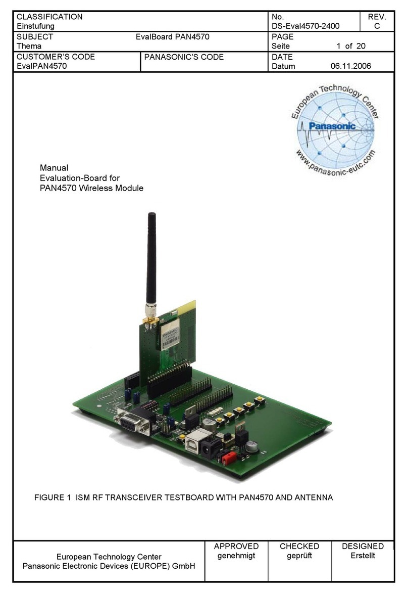
FIGURE 1 ISM RF TRANSCEIVER TESTBOARD WITH PAN4555 AND ANTENNA

CLASSIFICATION
Einstufung PRELIMINARY No.
DS-Eval4555-2400
REV.
01
SUBJECT
Thema
EvalBoard PAN4555
PAGE
Seite
2 of 16
CUSTOMER’S CODE
EvalPAN4555
PANASONIC’S CODE
DATE
Datum
30.03.2007
European Technology Center
Panasonic Electronic Devices (EUROPE) GmbH
APPROVED
genehmigt
CHECKED
geprüft
DESIGNED
Erstellt
TABLE OF CONTENTS
1. Overview .........................................................................................................................3
1.1. Contents of the Evaluation Kit: ..............................................................................3
1.2. Hardware needed ..................................................................................................3
1.3. Software needed....................................................................................................3
2. Setting up the EvalBoard ................................................................................................4
3. Testboard Layout ............................................................................................................5
4. Operation of the testboard ..............................................................................................6
5. Power Supply..................................................................................................................6
5.1. D.C. power from a power supply ...........................................................................6
5.2. D.C. power from a USB device:.............................................................................7
5.3. Power on................................................................................................................7
6. Serial Ports .....................................................................................................................8
7. Reset...............................................................................................................................8
8. BDM connector ...............................................................................................................8
8.1. Flashing and serial upload Instructions .................................................................9
9. Freescale ZigBee Implementation ................................................................................10
9.1. Development of Applications with freescale BeeStackTM.....................................10
9.2. RF Testing of PAN4555.......................................................................................11
10. Schematic of the TESTBOARD and PAN4555 pinlist...................................................12
10.1. Sheet 1 ................................................................................................................12
10.2. Sheet 2 ................................................................................................................13
10.3. PAN4555 pinlist ...................................................................................................14
11. Related Documents.......................................................................................................15
12. Document STATUS.......................................................................................................15
13. History for this Document..............................................................................................15
14. General Information ......................................................................................................16
15. Life Support Policy ........................................................................................................16

CLASSIFICATION
Einstufung PRELIMINARY No.
DS-Eval4555-2400
REV.
01
SUBJECT
Thema
EvalBoard PAN4555
PAGE
Seite
3 of 16
CUSTOMER’S CODE
EvalPAN4555
PANASONIC’S CODE
DATE
Datum
30.03.2007
European Technology Center
Panasonic Electronic Devices (EUROPE) GmbH
APPROVED
genehmigt
CHECKED
geprüft
DESIGNED
Erstellt
1. OVERVIEW
The EvalKit PAN4555 allows quick and versatile evaluation of the of the wireless module
PAN4555. Currently the Embedded Bootloader plus test software from Freescale Inc. is provided
for RF performance testing, as for example Packet Error Rate (PER). Testing requires
installation of the GUI TestToolTM from Freescale Inc. on a computer with 2 COM ports.
Remark: ZigBee sample application software for this EvalKit is under preparation and will be
provided with the next version of this CD.
1.1. CONTENTS OF THE EVALUATION KIT:
- 2 x ISM RF Transceiver Testboards
- 2 x PAN4555 mounted on a carrierboard
- 2 x 2,45GHz antennas with male SMA plugs
- 2 x RS-232 cables
- 2 x battery adaptors with cable for d. c. power supply
- 1 x CD ZigBee-Modem PAN4555 with software and documentation
1.2. HARDWARE NEEDED
- 12 x Batteries (AA size) or 2 supplies 6-9Vdc with 2mm plugs
- PC with at least 1 (preferably 2) free COM Ports
- a Flashing Device for the MC9S08GT60 (Recommended: P&E USB HCS08/HCS12 Multilink
adapter USB-ML-12 available through http://www.pemicro.com/) or at
http://www.freescale.com/ZigBee)
1.3. SOFTWARE NEEDED
a) Freescale TestToolTM from Freescale Inc. as on the CD included, folder 132xxEVKCD\Install.
The embedded bootloader is required for TestToolTM and already installed on PAN4555, for
reinstalling it with USB HCS08/HCS12 Multilink adapter USB-ML-12 use the file in the folder
\embedded_bootloader\embedded_bootloader_4555.s19.
Remark: All the files in the folder 132xxEVKCD are unchanged versions from Freescale Inc..
Because of different hardware platforms of freescale reference devices and PAN4555 they do
NOT apply to PAN4555 directly. Check for updates of this folder at
http://www.freescale.com/ZigBee)
b) Software Flash Utility; recommended is the P&E USB HCS08/HCS12 Multilink adapter
USB- ML-12 available through http://www.pemicro.com/ . See also folder
132xxEVKCD\Drivers.
c) For the development of software based on ZigBeeTM, IEEE802.15.4 or SMACTM the
Integrated Development Environment (IDE) MetrowerksTM CodeWarrior IDE from
www.metrowerks.com is required.
Important: To install and run the programs you need Administrator rights on the test PC

CLASSIFICATION
Einstufung PRELIMINARY No.
DS-Eval4555-2400
REV.
01
SUBJECT
Thema
EvalBoard PAN4555
PAGE
Seite
4 of 16
CUSTOMER’S CODE
EvalPAN4555
PANASONIC’S CODE
DATE
Datum
30.03.2007
European Technology Center
Panasonic Electronic Devices (EUROPE) GmbH
APPROVED
genehmigt
CHECKED
geprüft
DESIGNED
Erstellt
2. SETTING UP THE EVALBOARD
Plug a PAN4555 Carrierboard on one of the three 34-pins headers B,C or D as shown in Figures
1 and 2. Please take care that pin 1 of the Carrierboard connects to pin1 of the testboard
according to the “1” marking on the PCBs.
Important: Only 1 PAN4555 carrierboard may be plugged on the testboard.
The other 34-pin headers/sockets are provided for demo application boards like sensors,
actuators, etc. On slot A a socket is mounted instead of double pin rows for applications
using a plug with pins. For details on the testboard see chapter 3 and the testboard schematic in
chapter 10.
Mount the 50Ohms 2,4GHz antenna with SMA male plug on the PAN4555 SMA socket.
Set the +2,7Vdc supply jumper to the corresponding 2-pin header B-C-D.
Instead of a jumper an amperemeter for measuring the module current on VCC can be
connected.
Remark: In case of inserting an amperemeter the voltage drop at the amperemeters internal
resistor reduces the Vcc voltage applied to PAN4555 depending on the current drawn. Thus
check if the amperemeter used has an internal resistance of sufficiently low value.
In addition to a default +2,7Vdc Vcc supply a +5Vdc regulated voltage is available on the headers
(this does not apply to usage of USB as power supply) which could be useful for application
boards needing a higher supply voltage (i.e. with white LEDs). +5Vdc on the headers must be
activated by setting JP2.
Important: Do not connect the +5Vdc to PAN4555 directly.
The total available current from Vcc plus the current from +5Vdc is approximately 270mA
maximum, provided that the power source voltage applied to P1-P2-P3 does not drop below
approximately 6,6Vdc.
For the location of switches and jumpers on the Evaluation board see chapter 3.

CLASSIFICATION
Einstufung PRELIMINARY No.
DS-Eval4555-2400
REV.
01
SUBJECT
Thema
EvalBoard PAN4555 PAGE
Seite 5 of 16
MER’S CODE PANASONIC’S CODE
DATE
Datum
30.03.2007
CUSTO
EvalPAN4555
European Technology Center
Panasonic Electronic Devices (EUROPE) GmbH
APPROVED
genehmigt
CHECKED
geprüft
DESIGNED
Erstellt
3. TESTBOARD LAYOUT
power switch
power supply
inputs 7-9Vdc
JP2 for
connecting +5Vdc
to carrierboards
(not used on
PAN4551 board)
RESET button
BDM for
programming
Vcc voltage
selector, JP4 set
for 2,7Vdc
serial RS232
interface COM2
UART1: S1-1 and
S1-3 on, all others
off (no HW
handshake)
UART2: S1-2 and
S1-4 on, all others
off (no HW
handshake)
input buttons
output
LEDs
PAN4551 SMA socket
1
Figure 2 ISM RF Transceiver testboard with PAN4555 and antenna

CLASSIFICATION
Einstufung PRELIMINARY No.
DS-Eval4555-2400
REV.
01
SUBJECT
Thema
EvalBoard PAN4555
PAGE
Seite
6 of 16
CUSTOMER’S CODE
EvalPAN4555
PANASONIC’S CODE
DATE
Datum
30.03.2007
European Technology Center
Panasonic Electronic Devices (EUROPE) GmbH
APPROVED
genehmigt
CHECKED
geprüft
DESIGNED
Erstellt
4. OPERATION OF THE TESTBOARD
If not already done please follow the basic setting up instructions as in Chapter 2
Check if the jumper plugs are set as indicated in Figure 2. The functions of the jumpers are as
follows:
jumper name function to set as in Figure 2
A Vcc for module in Slot A* do not care
B Vcc for module in Slot B* do not care
C Vcc for module in Slot C* yes
D Vcc for module in Slot D* do not care
JP2 5Vdc feed to Slots A, B, C, D** no
JP3 Vcc setting 2.1-2.7-3.4V; see Table 2 no for Vcc=2.7Vdc default
JP4 Vcc setting 2.1-2.7-3.4V; see Table 2 yes for Vcc=2.7Vdc default
JP7 Vcc regulator output feed to A, B, C, D yes
(Table 1)
* An amperemeter for measuring module current can be inserted instead of the jumper
** +5Vdc supply (independent on JP3 and JP4 settings) option is provided for application demos.
It is not used on PAN4555 carrierboard.
Check if the port switches S1 near to the COM2 connector for RS232 are all set to off position
except the selected UART as noted in Figure 2/Table 3.
5. POWER SUPPLY
5.1. D.C. POWER FROM A POWER SUPPLY
Set the power switch SW7 to the position 2 = off.
Connect a power supply with 7-9VDC to one of the power inputs (P1 or P2).
In case of P1 use a plug with 5,5mm diameter and the positive terminal at the centre contact.
For use of the P2, 2mm contacts the black socket P2-X1 is the negative/ground contact and
the red socket P2-X2 is the positive terminal.
A linear regulator on the testboard regulates the input voltage down to the +5V DC board
supply. A second linear regulator regulates the +5V DC down to the module VCC supply of
2,1/2,7/3,4Vdc

CLASSIFICATION
Einstufung PRELIMINARY No.
DS-Eval4555-2400
REV.
01
SUBJECT
Thema
EvalBoard PAN4555
PAGE
Seite
7 of 16
CUSTOMER’S CODE
EvalPAN4555
PANASONIC’S CODE
DATE
Datum
30.03.2007
European Technology Center
Panasonic Electronic Devices (EUROPE) GmbH
APPROVED
genehmigt
CHECKED
geprüft
DESIGNED
Erstellt
5.2. D.C. POWER FROM A USB DEVICE:
In case no dedicated supply is available, DC supply can be taken from an USB connection.
The +5V DC from the USB feeds the linear regulator for the modules VCC supply of
2,1/2,7/3,4Vdc (see table 1).
Please note that communication via the USB connector is not possible.
Please take into account that when using the +5V DC feed to the 34-pin-headers in
combination with USB power supply the voltage is not +5V but unregulated 4.3 V DC due to
the voltage drop at a protection diode connected in series on the testboard.
Warning: Do not overload the USB power source. Check for the current available from
your USB device in order to avoid malfunction of or damage to your USB power source.
5.3. POWER ON
Set SW7 to the position 1 = on. (With power from USB position 1 is off and position 2 is on).
D7 should be lit indicating that +5Vdc supply is available on the testboard. D8 should be lit
indicating that the regulated Vcc module supply is available.
The dc regulator output voltage is set with a jumper on JP3 or JP4 as follows:
jumper on 2-pin header regulator output voltage VCC remarks
JP4 only 2,7 Vdc typical for PAN4555
JP3 only 3,4 Vdc maximum for PAN4555
no jumpers 2,1 Vdc minimum for PAN4555
(Table 2)

CLASSIFICATION
Einstufung PRELIMINARY No.
DS-Eval4555-2400
REV.
01
SUBJECT
Thema
EvalBoard PAN4555
PAGE
Seite
8 of 16
CUSTOMER’S CODE
EvalPAN4555
PANASONIC’S CODE
DATE
Datum
30.03.2007
European Technology Center
Panasonic Electronic Devices (EUROPE) GmbH
APPROVED
genehmigt
CHECKED
geprüft
DESIGNED
Erstellt
6. SERIAL PORTS
The evalboard is equipped with a serial port connector (COM2). The COM port can be linked to
either UART1 (SCI1) or UART2 (SCI2) on the module. This is done with the S1 switch, which has
to be set as follows:
UART1
active
1 2 3 4 5 6 7 8
SW1
settings
on off on off off off off off
UART2
active
1 2 3 4 5 6 7 8
SW1
settings
off on off on off off off off
(Table 3)
Remark: For PAN4555 only UART1 is used, SW1-2 and SW1-4 are have to be set to OFF.
7. RESET
Reset of the testboard and the boards at A,B,C or D can be done with the button named
“RESET” next to the USB socket.
8. BDM CONNECTOR
Reprogramming of PAN4555 can be done via the on-board BDM connector.
For programming, the P&E USB HCS08/HCS12 Multilink adapter USB-ML-12 available through
http://www.pemicro.com/ is recommended, but any programmer capable of flashing the
MC9S08GT60 Controller on the Module can be used.
The 6-pin BDM header has the same pinning as the Multilink adapter cable and is located
between the reset switch and the COM2 Connector.
Please make sure that pin1 of the plug connects to pin1 of the header. The correct device
selection for PAN4555 is a Motorola MC9S08GT60.

CLASSIFICATION
Einstufung PRELIMINARY No.
DS-Eval4555-2400
REV.
01
SUBJECT
Thema
EvalBoard PAN4555
PAGE
Seite
9 of 16
CUSTOMER’S CODE
EvalPAN4555
PANASONIC’S CODE
DATE
Datum
30.03.2007
European Technology Center
Panasonic Electronic Devices (EUROPE) GmbH
APPROVED
genehmigt
CHECKED
geprüft
DESIGNED
Erstellt
8.1. FLASHING AND SERIAL UPLOAD INSTRUCTIONS
Remark: Installation of the embedded bootloader and upload of the test software to
PAN4555 is already done and only required for re-installation
1. Download and install the required Software for USB HCS08/HCS12 Multilink adapter
USB-ML-12. See also folder 132xxEVKCD\Drivers\P&E USB device.
2. Plug the PAN4555 carrierboard on the testboard and switch the testboard power ON
3. Connect the USB HCS08/HCS12 Multilink adapter to the BDM connector on the
testboard and via USB to the PC where the flash programming software is
installed.
4. Start the HCS08 Flash Programmer and select as port the P&E HCS08/HCS12 Multilink
5. Select the 9S08GT60.S8P Algorithm to be used
6. Wait for the Flashing Utility to become ready
7. Erase the PAN4555 flash memory
8. Select the \embedded_bootloader\embedded_bootloader_4555.s19 file from the CD
9. Choose “program” to flash it into the PAN4555
10. Wait for completion of the programming algorithm
11. After removing the BDM connector push RESET on the Testboard.
The LEDs D13 and D14 should be lit permanently now.
12. Set the COM1 switch on the testboard to UART1, e. g. switch 1 and 3 ON and all others
OFF. Connect the testboard via a serial cable to the PC. Start the Freescale TestTool
13. Select Tools / Communication Settings / Add Internal with the COM Port you have the
Board connected to and as Baudrate choose 19200, then close the Window
14. Now select View / Embedded Bootloader and choose the COM Port you want to use
Wait several seconds until a board type window appears. Select 13213-NCB and OK.
From the Application files displayed select
“EVK_PTC_Demo_w_Embedded_Bootloader_V202_13213_NCB” and “UPLOAD”.
The upload progress is shown on the display with the final the message
“Firmware downloaded – resets system”
15. Close the Embedded Bootloader and open VIEW\ZigBee Radio Test
16. Check a “Device Ready”, a “Ping” has to result in “Hello”
17. Now the devices are ready for a test as in part 9.2

CLASSIFICATION
Einstufung PRELIMINARY No.
DS-Eval4555-2400
REV.
01
SUBJECT
Thema
EvalBoard PAN4555
PAGE
Seite
10 of 16
CUSTOMER’S CODE
EvalPAN4555
PANASONIC’S CODE
DATE
Datum
30.03.2007
European Technology Center
Panasonic Electronic Devices (EUROPE) GmbH
APPROVED
genehmigt
CHECKED
geprüft
DESIGNED
Erstellt
9. FREESCALE ZIGBEE IMPLEMENTATION
9.1. DEVELOPMENT OF APPLICATIONS WITH FREESCALE BEESTACKTM
PAN4555 is built around the MC13214 single package from Freescale Inc. which includes the
freescale ZigBee codebase BeeStackTM (downscaled versions of PAN4555 with MC1321x suited
for IEEE802.15.4 or SMAC only are available on demand as well).
The access to BeeStackTM is provided after registration and login at www.freescale.com/zigbee .
After login the BEEKITDOWNLOADPACKAGE.zip can be downloaded. This package contains
BeeStackTM , IEEE802.15.4 MAC and SMAC codebases. For PAN4555 PHY testing using
TestToolTM the download of the latest 1321xEVK package is recommended.
After successful installation of Beekit on a PC open BeeKit. A ZigBee sample solution *.bksln can
be created in a few steps.
Important: Before a solution may be exported for PAN4555 the MC1321x target settings have to
be changed via the “User defined target editor”. The required changes are:
1. Uncheck the “Use external Antenna Switch”
2. Adjust the port settings depending on your application, the PAN4555 datasheet and for
use of the PAN4555 carrierboard the pinlist in chapter 10.3.
For importing, compiling and debugging of the BeeKitTM solution the Integrated Development
Environment (IDE) MetrowerksTM CodeWarrior from www.metrowerks.com is required.
As device flash programmer the USB HCS08/HCS12 Multilink from www.pemicro.com is
recommended.
Important: PAN4555 is a single rf port design with MC13214, refer also to AN3248.
The Freescale reference boards 13213-NCB and 13213-SRB are dual port designs,
software for these boards will not run.
The shipping of products which use ZigBeeTM technology requires a membership of the ZigBeeTM
Alliance (www.zigbee.org), at least as an adopter member, and is mandatory for the ZigBeeTM
product certification procedure and use of the ZigBeeTM Logo.
The prices and fees as known from today are as follows:
1. IDE CodeWarrior order number CWS-H08-C64K-CX from www.metrowerks.com : US$ 995,-.
2. USB HCS08/HCS12 Multilink (www.pemicro.com), orderable at www.freescale.com/zigbee
with the ID USBMULTILINKBDM: US$ 99,-
3. BeeStackTM: The support fee after a 30 days period free of charge required by Freescale Inc.
is US$ 999,-.
4. Companies selling products using ZigBeeTM technology have to be a member of the
ZigBeeTM Alliance (www.zigbee.org). The minimum fee per year for a membership as adopter
is US$ 3500,-.
5. For adopter members the fee for listing the first product at (www.zigbee.org) is US$ 1000,-.
6. The cost of a ZigBeeTM product certification at a testhouse (TÜV Rheinland) ranges
from approximately US$ 4000,- to US$ 8000,-, depending on the implemented software.
CLASSIFICATION
Einstufung PRELIMINARY No.
DS-Eval4555-2400
REV.
01
SUBJECT
Thema
EvalBoard PAN4555
PAGE
Seite
11 of 16
CUSTOMER’S CODE
EvalPAN4555
PANASONIC’S CODE
DATE
Datum
30.03.2007
European Technology Center
Panasonic Electronic Devices (EUROPE) GmbH
APPROVED
genehmigt
CHECKED
geprüft
DESIGNED
Erstellt
9.2. RF TESTING OF PAN4555
refer also to: freescale\documentation\13213EVKUG.pdf on the CD
ZigBee radio testing can be done using the “Test Tool” on a PC. Operation and some often
used functions are described below:
1. Install TestTool (from folder 132xxEVKCD on CD) on a PC with a free COM port.
2. Set the Testboard COM port to UART1 and connect it to the PC
3. If needed (for example for PER measurements within ZigBee Radio Test
of TestTool) connect the second Testboard (set to UART1 too) to a second
free COM port of the PC. If your PC does not provide enough serial ports,
a USB to COM converter cable could help.
4. This step is only required for reprogramming:
Flash program the embedded_bootloader_4555.s19 via the BDM and upload the
EVK_PTC_Demo_w_Embedded_Bootloader_V202_13213_NCB via the serial cable to
PAN4555 as described in 8.1.
5. Push RESET on the testboard and open TestTool\View\ZigBee Radio Test.
6. Open TestToolTM and Push “PING” and “HOOK” for a device firmware test.
7. Important: In section “SPI Registers” read modem control_b register address x07,
the result is 0x4ca0. This content means dual port mode as for 13213-NCB devices.
Change this setting by writing 0x5ca0 to register x07, enabling the MC13214 internal
Rx/Tx switch for single port operation.
Remark: in case of missing rf input/output while testing with TestTool readout this
register in order to check if it is still set to 0x5ca0 .
8. RF Testing Tx mode
“ Set Continuous TX” with the result “Succeeded”. PAN4555 is set to a continuous
unmodulated carrier for testing of wanted and unwanted (e.g. harmonics)
output power or carrier frequency accuracy.
The related settings are:
- “Channel”, write for example 0x0b for the lowest frequency at 2405MHz or
0x1a for the highest frequency at 2480MHz.
- “Xtal Trim”, the readout value is 0x7e. For series production this value might be
adjusted for PAN4555
- “Spi Register 12”
The default readout 0xbc sets PAN4555 to a power of approximately –3dBm.
In order to check the harmonics power, write 0xff for maximum power of
approximately +1dBm at the carrier frequency.
9. RF Testing Rx mode
The most important parameter for Rx mode is the sensitivity determined by
increasing the path loss between transmitter and receiver until the Packet Error Rate
inrceases from 0 to 1% (with 20 bytes payload according to the IEEE802.15.4
requirements). For detailed information on how to run PER measurements refer to
the freescale documentation.
Remark: Make shure that both Transmitter and Receiver are set to single
port mode as described under point 7.

CLASSIFICATION
Einstufung PRELIMINARY No.
DS-Eval4555-2400
REV.
01
SUBJECT
Thema
EvalBoard PAN4555
PAGE
Seite
12 of 16
CUSTOMER’S CODE
EvalPAN4555
PANASONIC’S CODE
DATE
Datum
30.03.2007
European Technology Center
Panasonic Electronic Devices (EUROPE) GmbH
APPROVED
genehmigt
CHECKED
geprüft
DESIGNED
Erstellt
10. SCHEMATIC OF THE TESTBOARD AND PAN4555 PINLIST
10.1. SHEET 1

CLASSIFICATION
Einstufung PRELIMINARY No.
DS-Eval4555-2400
REV.
01
SUBJECT
Thema
EvalBoard PAN4555
PAGE
Seite
13 of 16
CUSTOMER’S CODE
EvalPAN4555
PANASONIC’S CODE
DATE
Datum
30.03.2007
European Technology Center
Panasonic Electronic Devices (EUROPE) GmbH
APPROVED
genehmigt
CHECKED
geprüft
DESIGNED
Erstellt
10.2. SHEET 2

CLASSIFICATION
Einstufung PRELIMINARY No.
DS-Eval4555-2400
REV.
01
SUBJECT
Thema
EvalBoard PAN4555
PAGE
Seite
14 of 16
CUSTOMER’S CODE
EvalPAN4555
PANASONIC’S CODE
DATE
Datum
30.03.2007
European Technology Center
Panasonic Electronic Devices (EUROPE) GmbH
APPROVED
genehmigt
CHECKED
geprüft
DESIGNED
Erstellt
10.3. PAN4555 PINLIST
The table below shows the connections provided via the PAN4555 carrierboard.
header
pin
testboard_V1_1, headers
B-D PAN4555 used on testboard as
1 5VDC not connected
2 PTG1 PTG1
3 NC7 not connected
4 NC6 not connected
5 PTE0 PTE0 TxD via S1
6 PTE1 PTE1 RxD via S1
7 PTC0 PTC0
8 PTC1 PTC1
9 PTD2 PTD2
10 NC5 not connected
11 PTC2 PTC2 D11
12 PTC5 PTC5 D12
13 PTA6 PTA6
14 PTA7 PTA7
15 PTB0 PTB0 SW2
16 PTA5 PTA5 SW3
17 PTB1 PTB1 SW4
18 PTB2 PTB2 SW5
19 VDDA VDDA
20 PTB7 PTB7
21 PTD6 PTD6 D13
22 PTD4 PTD4 D14
23 NC9 not connected
24 NC3 not connected
25 NC8 not connected
26 NC2 not connected
27 PTC3 PTC3
28 VCC VCC VCC
29 RESET RESET RESET
30 BKGD BKGD BKGD
31 NC4 not connected
32 NC1 not connected
33 GND GND
34 VREFH VREFH

CLASSIFICATION
Einstufung PRELIMINARY No.
DS-Eval4555-2400
REV.
01
SUBJECT
Thema
EvalBoard PAN4555
PAGE
Seite
15 of 16
CUSTOMER’S CODE
EvalPAN4555
PANASONIC’S CODE
DATE
Datum
30.03.2007
European Technology Center
Panasonic Electronic Devices (EUROPE) GmbH
APPROVED
genehmigt
CHECKED
geprüft
DESIGNED
Erstellt
11.RELATED DOCUMENTS
[1] Data sheet PAN4555 currently not available, under preparation,
see also PAN4555 flyer Web_PAN4555-B.pdf on the CD
[2] Data Sheet Freescale MC1321xDS - MC1320x 2.4 GHz Low Power Transceiver.pdf
[3] Data Sheet Freescale MC9S08GT60 Microcontroller
12.DOCUMENT STATUS
This information is preliminary.
13. HISTORY FOR THIS DOCUMENT
Revision
Version
Date
Datum
Modification / Remarks
Änderungen / Bemerkungen
01 30.03.2005 preliminary version

CLASSIFICATION
Einstufung PRELIMINARY No.
DS-Eval4555-2400
REV.
01
SUBJECT
Thema
EvalBoard PAN4555
PAGE
Seite
16 of 16
CUSTOMER’S CODE
EvalPAN4555
PANASONIC’S CODE
DATE
Datum
30.03.2007
European Technology Center
Panasonic Electronic Devices (EUROPE) GmbH
APPROVED
genehmigt
CHECKED
geprüft
DESIGNED
Erstellt
14.GENERAL INFORMATION
This product description does not lodge the claim to be complete and free of mistakes.
Please contact the related product manager in every case.
If we deliver samples to the customer, these samples have the status Engineering Samples.
This means, the design of this product is not yet concluded. Engineering Samples may be
partially or fully functional, and there may be differences to be published Data Sheet.
Engineering Samples are not qualified and are not to be used for reliability testing or series
production.
Waiver:
Customer acknowledges that samples may deviate from the Data Sheet and may bear defects
due to their status of development and the lack of qualification mentioned above.
Panasonic Electronic Devices (Europe) GmbH rejects any liability or product warranty for
Engineering Samples. In particular, Panasonic Electronic Devices (Europe) GmbH waives
liability for damages caused by
• the use of the Engineering Sample other than for Evaluation Purposes, particularly the
installation or integration in an other product to be sold by Customer,
• deviation or lapse in function of Engineering Sample,
• improper use of Engineering Samples.
Panasonic Electronic Devices (Europe) GmbH waives any liability for consequential and
incidental damages. In case of any questions, please contact your local sales partner or the
related product manager.
15.LIFE SUPPORT POLICY
This Panasonic Electronic Devices (Europe) GmbH product is not designed for use in life
support appliances, devices, or systems where malfunction can reasonably be expected to
result in a significant personal injury to the user, or as a critical component in any life support
device or system whose failure to perform can be reasonably expected to cause the failure of
the life support device or system, or to affect its safety or effectiveness. Customers using or
selling these products for use in such applications do so at their own risk and agree to fully
indemnify Panasonic Electronic Devices (Europe) GmbH for any damages resulting.
Table of contents
Other Panasonic Motherboard manuals

Panasonic
Panasonic PAN4570 User manual

Panasonic
Panasonic AN30182A-EVB User manual

Panasonic
Panasonic NN32251A User manual

Panasonic
Panasonic PGA26E07BA-SWEVB008 User manual

Panasonic
Panasonic EVB-NN30312A User manual

Panasonic
Panasonic AN33014UA User manual

Panasonic
Panasonic NN30320A User manual

Panasonic
Panasonic PAN9420 User manual

Panasonic
Panasonic PAN9320ETU User manual

Panasonic
Panasonic Grid-EYE User manual