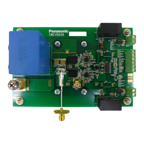
Panasonic PGA26E07BA-SWEVB006 User manual

PGA26E07BA-SWEVB006 Ver. 1.2 1
PGA26E07BA-SWEVB006
Chopper Evaluation Board consisting:
1. PGA26E07BA 600V 56mΩ X-GaN Power Transistor
2. AN34092B Single channel X-GaN Gate Driver IC
For evaluation of X-GaN Power Transistor and Driver switching characteristics
The products and product specifications described in the
document are subject to change without notice for modification
and/or improvement. At the final stage of your design,
purchasing, or use of the products, please request for the up-
to-date Product Standards in advance to ensure that the latest
specifications meet your requirements.
Panasonic Semiconductor Solutions Co. Ltd.
1 Kotari-yakemachi, Nagaokakyo, Kyoto 617-8520, Japan
http://www.semicon.panasonic.co.jp/en/

PGA26E07BA-SWEVB006 Ver. 1.2 2
Contents
Features……………………………………………………………………………………………………………………………………………………….3
Description of the Evaluation Board……………………………………………………………………………………………………………..4
Recommended Operating Conditions…………………………………………………………………………………………………………..4
Schematic Diagram……………………………………………………………………………………………………………………………………….5
Bill of Materials…………………………………………………………………………………………………………………………………………….5
Appearance………………………………………………………………………………………………………………………………………………….7
PCB Layout…………………………………………………………………………………………………………………………………………………..8
Test circuits………………………………………………………………………………………………………………………………………………….9
Equipment………………………………………………………………………………………………………………………………………………….10
Measurement Procedures………………………………………………………………………………………………………………………….11
Measurement Results………………………………………………………………………………………………………………………………..13
Important Notice……………………………………………………………………………………………………………………………………….15

PGA26E07BA-SWEVB006 Ver. 1.2 3
Features
X-GaN Gate Driver
█Supports high switching frequency (~4MHz)
█Achieved safe operation
- negative voltage source, active miller clamp
█Facilitate gate drive design
- high precision gate current source
X-GaN Transistor
█Blocking Voltage: 600V
█ Pulse Peak IDS: 61A
█IDS (cont): 31A
█ RDS(on) typ: 56mΩ
█ Normally Off Device
Source2Source1
Source
Drain
Gate
PGA26E07BA
AN34092B
Propagation
Delay
30ns

PGA26E07BA-SWEVB006 Ver. 1.2 4
Description of the Evaluation Board
The PGA26E07BA-SWEVB006 is a chopper evaluation board using a dedicated X-GaN driver
(AN34092B) for measuring the high speed switching characteristics of turn-on and turn-off of the X-
GaN power transistor. The dv/dt and di/dt using an inductive load can be measured by controlling
the X-GaN power transistor with an external signal. There are test terminals prepared for easy
monitoring of Vgs and Vds waveforms. To improve the accuracy of the current measurement, use
the mounted semi-rigid connector and connect to a 50Ω terminated oscilloscope input. The
evaluation board together with the user’s guide also serves as a reference design for the X-GaN
gate driver circuit and PCB layout.
Recommended Operating Conditions
Table 1 shows the operating conditions used to achieve the switching performance reported in the
Measurement Result. All the components used in the evaluation board are rated for the
recommended operating conditions only.
Please read the measurement procedure before starting the evaluation. It is necessary to refer to
the X-GaN transistor and driver datasheet when using this user’s guide. The detail operation of the
gate driver IC and the design of its peripheral components are described in the OPERATION
section of the datasheet.
Table 1: Recommended operating conditions
Parameter
Condition
Input voltage (DC power ①)
400V
Driver IC power supply voltage (DC power ②)
12V
External clock voltage
(pulse generator input)
5V
External clock frequency (Duty Cycle)
(pulse generator input)
Double pulse
(Do not perform continuous operation)
External inductor
95uH @ DC Current=15A
Temperature
25ºC
①② Power supply equipment number as illustrated on page 9 and 10
PGA26E07BA-SWEVB006 Ver. 1.2 5
Schematic Diagram
Refer to Figure 1 below for the circuit schematic of the evaluation board. All the terminals and
components shown are mounted on the evaluation board including the power inductor.
Figure 1: Schematic diagram of evaluation board
Bill of Materials
Table 2: Bill of Materials
Parts
Symbol
Specification
Part Number
Manufacturer
Package
Chip
Resistor
R1
8.2Ω
ERJ3GEYJ8R2V
Panasonic
SMD1608
R3
1.0Ω
ERJ3GEYJ1R0
Panasonic
SMD1608
R5
39kΩ
ERJ3EKF3902V
Panasonic
SMD1608
R9
47kΩ
ERJ3EKF4702V
Panasonic
SMD1608
R12
47mΩ
RL7520WR-R047-F
Susumu
SMD3008
Chip
Capacitor
C0
2.2uF / 450V
ECWFE2W225K
Panasonic
Radial Thru Hole
C1
0.47uF / 630V
C5750X7T2J474K
TDK
SMD5750
C2
2200pF / 50V
GRM1885C1H222JA01
Murata
SMD1608
C3
220nF / 25V
GRM188R71E224KA88
Murata
SMD1608
C4
0.47uF / 16V
GRM188R71C474KA88
Murata
SMD1608
C5
4.7uF / 16V
GRM21BB31E475K
Murata
SMD1608

PGA26E07BA-SWEVB006 Ver. 1.2 6
Parts
Symbol
Specification
Part Number
Manufacturer
Package
Chip
Capacitor
C6
1uF / 25V
GRM188B31E105KA75
Murata
SMD1608
C9
10uF / 35V
GRM32ER7YA106KA12
Murata
SMD3225
C10
0.1uF / 50V
GRJ188R71H104KE11D
Murata
SMD1608
Rectifier
Diode
D1
1200V / 12A
C4D08120E
CREE
TO-252
DPAK
Inductor
L1
95uH
LHDM010101DYBV1E
Nippon Chemicon
Screw
Terminal
CON1
-
OP-045-M4
Osada
Terminal
Block
CON2
-
1727052
Phoenix Contact
Semi-rigid
-
SMA(PJ)-X-UT47-63
APEX Technology
GaN
Transistor
Q1
600V / 56mΩ
PGA26E07BA
Panasonic
SMD (8x8)
Gate Driver
IC1
Gate driver
AN34092B
Panasonic
QFN (4x4)

PGA26E07BA-SWEVB006 Ver. 1.2 7
Appearance
Double-sided
Size: 100mm × 70mm
Copper thickness: 70um
Board thickness: 1.6mm
Figure 2: Top Side View
Figure 3: Bottom Side View
R12
Q1 Drain current sense resistor
DC power ①
Input terminal
Pulse generator
Input terminal
(Non-inverting input)
L1
Inductor
DC power ②
Input terminal
Inverting input is
connected to GND
DC power ①
Input terminal
D1
Rectifier Diode
IC1
X-GaN Driver IC
(AN34092B)
Q1
GaN Transistor
C1
Input Capacitor
C0
Input Capacitor

PGA26E07BA-SWEVB006 Ver. 1.2 8
PCB Layout
Figure 4: Top Layer
Figure 5: Bottom Layer
P
OUT
Pulse generator
connection points
DC power ①
connection points
DC power②
connection points
P
N
DC power ①
connection points
Pulse generator
connection points
GND
VCC
DC power②
connection points
IN+
GND
P
N
IN+
GND
GND
VCC

PGA26E07BA-SWEVB006 Ver. 1.2 9
Test circuits
Figure 6 shows the evaluation test circuit schematic with all the necessary connections. Figure 7
shows the actual evaluation board with all the terminals for connecting to the equipment. For detail
description of the connection, refer to Measurement Procedures on page 11.
Figure 6: Setup of Evaluation Environment
Figure 7: Connectors of Evaluation Board
Top View
Full View
DC power ①
DC power ②
(12V)
Pulse
Generator
Coil wire for
VDS monitoring
Coil wire for
VGS monitoring

PGA26E07BA-SWEVB006 Ver. 1.2 10
Equipment
The equipment used in the evaluation test circuits is shown in Table 3. This is for reference only.
Table 3: List of Equipment used
No.
Equipment
Specifications
Suggested Model
1
DC Power ①
OUTPUT
DC640V 1600W
Takasago ZX-400H
2
DC Power ②
OUTPUT
DC18V 1.5A
Kenwood PW18
3
*Pulse Generator
-
Agilent 33220A
4
**Oscilloscope
-
Tektronix DPO7104C
5
Probe
-
TCP0030 Current Probe
-
P6139B Voltage Probe
*Use only burst mode function from the pulse generator. Do not use continuous pulse mode as
this will cause damage to the components and evaluation board.
**For VGS and VDS monitoring, use the coil wire mounted on the evaluation board to minimize
any ringing in the waveform.

PGA26E07BA-SWEVB006 Ver. 1.2 11
Figure 8: Usage of coil wire
Measurement Procedures
Initial steps:
Do all the necessary connection between the
evaluation board, components and equipment.
Connect DC power ①to P/N of the board
with the terminal block.
Connect pulse generator to the IN+/GND
terminal of the board.
The IN- terminal must be shorted to GND
and not possible to input any signal.
Connect DC power ②to VCC/GND terminal
of the board.
Probe the point where you want to monitor
and observe the waveform using oscilloscope.
Be careful not to short with other parts. Use the coil wire fixture mounted on the evaluation
board for VGS, VDS1 & VDS2 monitoring.
Start-up:
Set up the pulse generator with the amplitude 0-5V and having the double pulse profile as
shown below:
Table 4: Double Pulse Setting with L=95uH
Figure 9: Double Pulse Profile
Again, ensure that the pulse generated occurs only in the burst mode. If the pulse is generated
continuously, the transistor will be damaged by high current flows.
Set the DC power ②to 12V gradually.
Check VGS waveform when a double pulse is inputted from pulse generator. Please carry out
this step with DC power ①is set to 0V.
Then, the voltage of DC power ①is gradually increased from 0V to predetermined voltage
(400V). Monitor the VDS1 voltage with oscilloscope and confirm that the VDS1 voltage rises to
the set value.
Input a double pulse with the pulse generator again and check the VGS, VDS1 and IL
waveform.
Observation of waveform will be easier if the trigger is applied at the rising / falling edge of
VGS or VDS1 as shown on Figure 9 above.
If different inductor value is used other than the one provided, please set the pulse width until
the desired IL value is achieved.
IL
#1
2.5A
0.6us
5A
1.3us
10A
2.6us
15A
3.8us
:Monitoring Point
2.5A/5A/10A/15A
IL
Drive Signal
VDS
0V
5V
#1
5u
s
0.8us

PGA26E07BA-SWEVB006 Ver. 1.2 12
T-off
400V
0V
40V
360V
VDS at
Turn Off
VDS at
Turn On
T-on
Shutdown:
Set the DC power ①slowly to 0V and then follow by the DC power ②to 0V.
Turn off the power. Check the VDS waveform and ensure that the capacitor between P/N
terminals has fully discharged. There is risk of electric shock due to the residual charge.
Measurement of dV/dt for Turn On/Off Switching Characteristics:
The range used is 10%~90%
IL condition is set at 2.5A / 5A / 10A / 15A with 16 times averaging
Therefore, the dv/dt at turn on: 320V / T-on and
the dv/dt at turn off: 320V / Toff
Figure 10: Measurement of dv/dt
Figure 11: Measurement points
VDS probe
connection
VGS probe
connection
Current probe for
IL monitoring

PGA26E07BA-SWEVB006 Ver. 1.2 13
Measurement Results
Condition: VPN=400V, VCC=12V, R1:8.2Ω, R3:1Ω, C2:2200pF
i) dV/dt Measurement Data
ii) VGS, VDS and IDS Measurement Waveform
VPN=400V,Ids=2.5A
VPN=400V,Ids=5A
Turn
ON
dV/dt =-123.1 [V/ns]
dV/dt=-114.1 [V/ns]
Turn
OFF
dV/dt=14.9 [V/ns]
dV/dt=31.3 [V/ns]
[Results are for reference only and measured data maybe different depending on evaluation environment]
VGS 4V/div
IL 5A/div
VDS 100V/div
Time scale: 10ns/div
5GS/s
Time scale: 10ns/div
5GS/s
Time scale: 10ns/div
5GS/s
Time scale: 10ns/div
5GS/s
VGS 4V/div
IL 5A/div
VDS 100V/div
VGS 4V/div
IL 5A/div
VDS 100V/div
VGS 4V/div
IL 5A/div
VDS 100V/div

PGA26E07BA-SWEVB006 Ver. 1.2 14
VPN=400V,Ids=10A
VPN=400V,Ids=15A
Turn
ON
dV/dt=-101.9 [V/ns]
dV/dt=-92.8 [V/ns]
Turn
OFF
dV/dt=62.9 [V/ns]
dV/dt=94.3 [V/ns]
Time scale: 10ns/div
5GS/s
Time scale: 10ns/div
5GS/s
Time scale: 10ns/div
5GS/s
Time scale: 10ns/div
5GS/s
VGS 4V/div
IL 5A/div
VDS 100V/div
VGS 4V/div
IL 5A/div
VDS 100V/div
VGS 4V/div
IL 5A/div
VDS 100V/div
VGS 4V/div
IL 5A/div
VDS 100V/div

PGA26E07BA-SWEVB006 Ver. 1.2 15
Important Notice
Please read and understand the following items, "Restriction", and "Caution" before using the evaluation
board:
Restriction
The evaluation board is intended for use as engineering development, verification or evaluation purposes
only.
This evaluation board is not intended for a finished end-product fit for general consumer use.
Do not operate in condition other than the recommended settings.
The evaluation board must be used only by qualified engineers and technicians that have electronics
training, familiar with handling of high-voltage electrical systems and observe good engineering practise
standards.
The evaluation board is meant to be operated in lab environment under the safe conditions.
Please use a protective case (accessory) during evaluation.
All of the specifications and evaluation data in this manual are for reference only and not guaranteed. The
information may subject to change without notice. Please contact to Panasonic representative for the
latest information.
The user assumes all responsibility and liability for proper and safe handling of this evaluation board.
Further, the user indemnifies Panasonic from all claims arising from the handling or use of the evaluation
boards.
The technical information described in this document is intended only to show the main characteristics
and application circuit examples of the products. No license is granted in and to any intellectual property
right or other right owned by Panasonic Corporation or any other company. Therefore, no responsibility is
assumed by our company as to the infringement upon any such right owned by any other company which
may arise as a result of the use of technical information described in this document.
Caution
The evaluation board carries hazardous high voltage. Do not touch when power is applied. Otherwise, it
may cause severe injury, disability or death.
Electric charge may be accumulated in the capacitors. To prevent electrical shock, please ensure all the
capacitors are properly discharged before touching the evaluation board.
It is the user’s responsibility to confirm that the voltages, isolation requirements, and rated value are
identified and understood, prior to handling the evaluation board.
Do not leave the evaluation board unattended while power is applied and do not perform other activity
near the evaluation board while power is applied.
This board contains parts that are susceptible to damage by electrostatic discharge (ESD). It is the user’s
responsibility to take any and all appropriate precautions with regard to electrostatic discharge when
using the evaluation board.
Should the evaluation board does not meet the specification indicated in the User’s Guide, the board may
be exchanged with a new one within 30 days from the date of delivery. When exchanging the evaluation
board, please return the board with all items included.
The warranty on this evaluation board is considered void once a part on the board is removed or modified.
The evaluation board does not fall within the scope of the technical requirements of the following
directives or other related directives:
- Restriction of Hazardous Substances (RoHS)
- Directive on Waste Electrical and Electronic Equipment (WEEE)
- Mandatory conformity marking for products sold in the European Economic Area (CE)
- Federal Communications Commission (FCC)
- Underwriters Laboratories, Inc. (UL)

PGA26E07BA-SWEVB006 Ver. 1.2 16

Request for your special attention and precautions
in using the technical information and semiconductors described in this book
(1) If any of the products or technical information described in this book is to be exported or provided to non-residents, the
laws and regulations of the exporting country, especially, those with regard to security export control, must be observed.
(2) The technical information described in this book is intended only to show the main characteristics and application circuit
examples of the products. No license is granted in and to any intellectual property right or other right owned by
Panasonic Corporation or any other company. Therefore, no responsibility is assumed by our company as to the
infringement upon any such right owned by any other company which may arise as a result of the use of technical
information de-scribed in this book.
(3) The products described in this book are intended to be used for general applications (such as office equipment,
communications equipment, measuring instruments and household appliances), or for specific applications as expressly
stated in this book.
Please consult with our sales staff in advance for information on the following applications, moreover please exchange
documents separately on terms of use etc.: Special applications (such as for in-vehicle equipment, airplanes, aerospace,
automotive equipment, traffic signaling equipment, combustion equipment, medical equipment and safety devices) in
which exceptional quality and reliability are required, or if the failure or malfunction of the products may directly
jeopardize life or harm the human body.
Unless exchanging documents on terms of use etc. in advance, it is to be understood that our company shall not be held
responsible for any damage incurred as a result of or in connection with your using the products described in this book
for any special application.
(4) The products and product specifications described in this book are subject to change without notice for modification
and/or improvement. At the final stage of your design, purchasing, or use of the products, therefore, ask for the most up-
to-date Product Standards in advance to make sure that the latest specifications satisfy your requirements.
(5) When designing your equipment, comply with the range of absolute maximum rating and the guaranteed operating
conditions (operating power supply voltage and operating environment etc.). Especially, please be careful not to exceed
the range of absolute maximum rating on the transient state, such as power-on, power-off and mode-switching. Other-
wise, we will not be liable for any defect which may arise later in your equipment.
Even when the products are used within the guaranteed values, take into the consideration of incidence of break down
and failure mode, possible to occur to semiconductor products. Measures on the systems such as redundant design,
arresting the spread of fire or preventing glitch are recommended in order to prevent physical injury, fire, social damages,
for example, by using the products.
(6) Comply with the instructions for use in order to prevent breakdown and characteristics change due to external factors
(ESD, EOS, thermal stress and mechanical stress) at the time of handling, mounting or at customer's process. We do
not guarantee quality for disassembled products or the product re-mounted after removing from the mounting board.
When using products for which damp-proof packing is required, satisfy the conditions, such as shelf life and the elapsed
time since first opening the packages.
(7) When reselling products described in this book to other companies without our permission and receiving any claim of
request from the resale destination, please understand that customers will bear the burden.
(8) This book may be not reprinted or reproduced whether wholly or partially, without the prior written permission of our
company.
No.010618
Table of contents
Other Panasonic Motherboard manuals

Panasonic
Panasonic Grid-EYE User manual

Panasonic
Panasonic EVB-NN30312A User manual

Panasonic
Panasonic PAN4570 User manual

Panasonic
Panasonic PAN9520 User manual

Panasonic
Panasonic PAN1311/21 USB User manual

Panasonic
Panasonic NN30320A User manual

Panasonic
Panasonic AN30182A-EVB User manual

Panasonic
Panasonic PAN9320ETU User manual

Panasonic
Panasonic EvalBoard PAN4555 User manual

Panasonic
Panasonic AN33014UA User manual