Pentek 52741 User manual

Pentek Model 52741 Installation Manual Page 1
Manual Part No: 800.52741 Rev: 2.1 −June 9, 2016
Pentek, Inc.
One Park Way
Upper Saddle River, NJ 07458
(201) 818−5900
http://www.pentek.com
Copyright © 2014−2016
INSTALLATION MANUAL
MODEL 52741
2−Channel 1.8 GHz A/D / 1−Channel 3.6 GHz D/A
with Digital Downconverter
Onyx®Family VPX Board

Page 2 Pentek Model 52741 Installation Manual
Warranty
Pentek warrants that all products manufactured by Pentek conform to published Pentek specifications and are free from defects in mate−
rials and workmanship for a period of one year from the date of delivery when used under normal operating conditions and within the
service conditions for which they were furnished. The obligation of Pentek arising from a warranty claim shall be limited to repairing or
at its option, replacing without charge, any product that in Pentek’s sole opinion proves to be defective within the scope of the warranty.
Pentek must be notified in writing of the defect or nonconformity within the warranty period and the affected product returned to Pentek
within thirty days after discovery of such defect or nonconformity. Buyer shall prepay shipping charges, taxes, duties and insurance for
products returned to Pentek for warranty service. Pentek shall pay for the return of products to buyer except for products returned from
another country.
Pentek shall have no responsibility for any defect or damage caused by improper installation, unauthorized modification, misuse, neglect,
inadequate maintenance, or accident, or for any product that has been repaired or altered by anyone other than Pentek or its authorized
representatives.
The warranty described above is buyer’s sole and exclusive remedy and no other warranty, whether written or oral, is expressed or
implied. Pentek specifically disclaims fitness for a particular purpose. Under no circumstances shall Pentek be liable for any direct, indi−
rect, special, incidental, or consequential damages, expenses, losses or delays (including loss of profits) based on contract, tort, or any
other legal theory.
Copyrights
With the exception of those items listed below, the contents of this publication are Copyright © 2014−2016, Pentek, Inc. All Rights
Reserved. Contents of this publication may not be reproduced in any form without written permission.
Trademarks
Pentek, Onyx, GateXpress, GateFlow, and ReadyFlow are registered trademarks or trademarks of Pentek, Inc.
OpenVPX is a trademark of VITA. PCI, PCI Express, PCIe, and PCI−SIG are trademarks or registered trademarks of PCI−SIG. Xilinx and
Virtex are registered trademarks or trademarks of Xilinx, Inc.
Manual Revision History
Date Revision Comments
1/6/14 1.0 Initial release.
3/13/14 1.1 Revised the default maximum speed to Gen 3 in Sect 2.4.
5/8/14 1.2 Removed references to Model 71740. Revised references to user manuals.
5/14/14 1.3 Corrected LEDs D1−D4 and JTAG connector locations on the carrier PCB by revising the following figures
and associated text: Figure 2−2, Figure 2−5, Figure 2−6, Figure 2−7, Figure 2−8.
6/6/14 1.4 Revised Sect 2.13.3 to resolve KB Case 1440.
9/15/14 1.5 Removed “factory use only” from sections about jumper JB1 and JTAG connector (Sect 2.6.1, Sect 2.9.7).
10/13/14 1.6 Sect 1.6, corrected the estimated power consumption. Sect 2.12.2, corrected analog full−scale input: +2
dBm to +4 dBm, programmable. Sect 2.12.2, corrected analog signal inputs IN2 and IN1 operation and use.
12/29/14 1.7 Corrected the number of pairs and lines from the PMC P14 connector to the VPX P2 connector (for Option
104) in Sect 1.5, Sect 1.6, Sect 2.9.2, Sect 2.9.6, Figure 1−1, Figure 2−8, and Table 2−10.
3/17/15 1.8 Sect 1.6, corrected the XMC power consumption.
4/3/15 1.9 Sect 2.9.3, added description of carrier OpenVPX Slot Profile.
6/5/15 1.10 Revised the installation procedure in Sect 2.10 to indicate that two VPX slots are required for installation.
6/18/15 2.0 Sect 1.6, changed Option 703 to 763. Sect 2.11, removed Option 703.
6/9/16 2.1 Sect 2.12.2, added value for the maximum input to the A/D to resolve KB Case 1528.
Printed in the United States of America.

Pentek Model 52741 Installation Manual Page 3
Page
Table of Contents
Rev.: 2.1
Chapter 1: Introduction
1.1 General Description..............................................................................................................................5
1.2 Features ..................................................................................................................................................5
1.3 Model 52741 Documentation ..............................................................................................................5
1.4 Block Diagram.......................................................................................................................................6
Figure 1−1: Model 52741 Block Diagram.........................................................................................6
1.5 Principle of Operation..........................................................................................................................7
1.6 Specifications.........................................................................................................................................8
Chapter 2: Installation and Connections
2.1 Inspection.............................................................................................................................................11
Figure 2−1: Model 52741 VPX Assembly.......................................................................................11
2.2 Jumper and Switch Settings ..............................................................................................................12
2.3 Removing XMC Module from VPX Carrier ..................................................................................13
Figure 2−2: Removing 71741 XMC from VPX carrier..................................................................13
2.4 XMC Module Switches ......................................................................................................................14
Figure 2−3: Model 71741 PCB Switches, Solder Side .................................................................14
Table 2−1: SW1 −FPGA Configuration ........................................................................................15
Table 2−2: FPGA Configuration Select −Switches SW1−3:4....................................................15
2.5 XMC Module LEDs ............................................................................................................................16
Figure 2−4: Model 71741 Main PCB, Solder Side LEDs.............................................................16
Table 2−3: XMC PCB LED Use........................................................................................................17
2.6 VPX Carrier Jumpers..........................................................................................................................18
Figure 2−5: Model 5201 VPX Carrier PCB, Connector Side.......................................................18
2.6.1 XMC JTAG −Jumper Block JB1 ......................................................................................19
Table 2−4: XMC JTAG −Jumper Block JB1 ................................................................19
2.6.2 XMC Reset Source −Jumper JB3 ....................................................................................19
Table 2−5: XMC Reset Source −Jumper JB3 ...............................................................19
2.6.3 XMC MVMRO −Jumper JB4 ..........................................................................................19
Table 2−6: XMC MVMRO −Jumper JB4 .....................................................................19
2.7 VPX Carrier Switches.........................................................................................................................20
Figure 2−6: Model 5201 VPX Carrier PCB, Solder Side..............................................................20
2.7.1 Clock Driver −Switch SW1 .............................................................................................21
Table 2−7: SW1 −Clock Driver Operation ..................................................................21
2.7.2 XMC Geographic Address −Switch SW2 .....................................................................21
Table 2−8: SW2 −XMC Geographic Address .............................................................21
2.8 VPX Carrier LEDs...............................................................................................................................22
Figure 2−7: Model 5201 VPX Carrier PCB, Solder Side..............................................................22

Page 4 Pentek Model 52741 Installation Manual
Page
Table of Contents
Rev.: 2.1
Chapter 2: Installation and Connections (continued)
2.9 VPX Carrier Connectors.................................................................................................................... 23
Figure 2−8: VPX Carrier Signal Connectors................................................................................. 23
2.9.1 XMC Connectors .............................................................................................................. 23
2.9.2 PMC Connector ................................................................................................................ 23
2.9.3 Carrier VPX Interface ....................................................................................................... 24
Figure 2−9: 5201 Carrier VPX Slot Profile.................................................................... 24
2.9.4 VPX P0 Utility Connector ............................................................................................... 25
2.9.5 VPX P1 Payload Connector ............................................................................................ 25
Table 2−9: VPX P1 Connector Pin Mapping ............................................................... 25
2.9.6 VPX P2 Module Connector (Option 104) ...................................................................... 26
Table 2−10: VPX P2 Connector Pin Mapping ............................................................. 26
2.9.7 Pentek JTAG Connector .................................................................................................. 27
Table 2−11: Pentek JTAG J5 Connector....................................................................... 27
2.10 Installing the Model 52741 in a VPX Card Cage............................................................................ 28
2.11 VPX Carrier Front Panels.................................................................................................................. 29
Figure 2−10: Model 52741 VPX Carrier Front Panels................................................................. 29
2.12 XMC Panel Connections.................................................................................................................... 30
Figure 2−11: 71741 XMC Front Panel............................................................................................ 30
2.12.1 PPS Input Connector ........................................................................................................ 30
2.12.2 Analog Input Connectors ................................................................................................ 30
2.12.3 Clock Input Connector ....................................................................................................31
2.12.4 Sync Bus Connector ......................................................................................................... 31
Table 2−12: SYNC/GATE Connector Pins................................................................... 31
2.13 XMC Panel LEDs................................................................................................................................ 32
2.13.1 PPS LED ............................................................................................................................. 32
2.13.2 Over Temperature LED ................................................................................................... 32
2.13.3 Link LED ............................................................................................................................ 32
2.13.4 ADC Overload LED .........................................................................................................32
2.13.5 Clock LED .......................................................................................................................... 32

Pentek Model 52741 Installation Manual Page 5
Rev: 2.1
Chapter 1: Introduction
1.1 General Description
Pentek’s Onyx®Family Model 52741 is a multichannel, high−speed analog data con−
verter. Using the VPX 3U card format, the 52741 includes a 3.6 GHz, 12−bit A/D con−
verter and four banks of memory.
The Model 52741 consists of one Pentek Model 71741 XMC module with a Pentek−sup−
plied FPGA IP core, mounted on a Pentek Model 5201 3U VPX carrier, assembled and
tested as a single board. It is ready to plug into a chassis with a single 3U VPX slot. The
FPGA core consists of a multiband digital downconverter.
1.2 Features
•1−channel mode with 3.6 GHz, 12−bit A/D
•2−channel mode with 1.8 GHz, 12−bit A/D per channel
• Xilinx®Virtex®−7 FPGA, with Pentek digital downconverter IP core
•GateXpress
®configuration manager supports dynamic FPGA reconfiguration
across the PCIe interface
• 4 GB of DDR3 SDRAM
• Sync bus for multimodule synchronization
• PCI Express®(PCIe®) (Gen 1, 2, or 3) interface up to x4 wide
• Optional user configurable gigabit serial interface
• Optional LVDS connections to the Virtex−7 FPGA for custom I/O
• VITA 42.0 XMC compatible with switched fabric interfaces
• Ruggedized and conduction−cooled versions available
1.3 Model 52741 Documentation
This Model 52741 Installation Manual describes the installation and connections for the
52741 VPX assembly. Documentation of the 71741 XMC operation and programming is
provided in the supplied Model 71741 Operating Manual, Pentek document 800.71741.
Datasheets for the programmable devices on Model 71741 are provided in the Pentek
Model 7x741 Series Supplemental Manual, part number 809.7x741. This document is
available on the CD provided by Pentek, in file 8097x741.pdf (PDF format).

Page 6 Pentek Model 52741 Installation Manual
Rev: 2.1
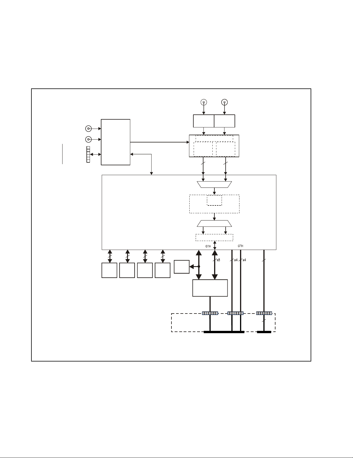
1.4 Block Diagram
The following is a simplified block diagram of Model 52741.
ClockGate/
PPS
TIMING
CONTROL
IN 1
RF In
RF
XFORMER
Gate In
Clk Reset In
RefClk In
RefClk Out
Sample Clk /
Reference Clk In
A/D Timing Bus
PPS In
IN 2
RF In
RF
XFORMER
12
1.8GHz
12-BITA/D 1.8GHz
12-BITA/D
Input Mux
A
DC12D1800
A
/D Converter
12
GATE/SYNC
DDC
ADCAcquisition Module
Interleave
PCI Express Interface
Deinterleave
Virtex-7 FPGA
GTH LVDS
32
32
DDR3
SDRAM
1 GB
DDR3
SDRAM
1 GB
32
32
DDR3
SDRAM
1 GB
DDR3
SDRAM
1 GB
24 pairs
Gigabit
Serial I/O
(option 105)
FPGA
GPIO
(option 104)
P14
PMC
P16
XMC
P15
XMC
PCIe
Gen 3
GATEXPRESS PCIe
CONFIGURATION
MANAGER
CONFIG
FLASH
1 Gb
FPGA
Config
Bus
PCIe
Gen3
P2P1
VPX VITA46 Backplane
24
pairs
x4
Model 5201
VPX Carrier
x4x4
Figure 1−1: Model 52741 Block Diagram

Pentek Model 52741 Installation Manual Page 7
Rev: 2.1
1.5 Principle of Operation
The Model 52741 consists of one Pentek Model 71741 XMC module mounted on a Pen−
tek Model 5201 VPX carrier, assembled and tested as a single board. The Model 71741
XMC has a Pentek−supplied FPGA digital downconverter IP core. The Model 52741 is
ready to plug into a chassis with a single 3U VPX slot.
The 71741 XMC includes a single−channel 3.6−GHz A/D converter or a two−channel
1.8−GHz A/D converter. Depending on the ADC operating mode (DES or non−DES),
the ADC processes either a single analog input using two A/D channels, or two analog
inputs using separate A/D channels, and sends the digital output from both channels
to the 71741 FPGA as separate data streams. The 71741 FPGA interleaves the two data
streams for processing by the ADC acquisition module and the digital downconverter
core.
The 71741 XMC features a Xilinx Virtex−7 FPGA for signal interfaces and processing.
The FPGA is pre−configured with a digital down−converter IP core. This FPGA also
provides board interfaces including PCIe and XMC. Custom I/O connections are pro−
vided to the FPGA through the optional PMC P14 connector (Option 104). Custom
gigabit serial interfaces may be implemented through the optional XMC P16 connector
(Option 105).
The 71741 includes 4 GBytes of DDR3 SDRAM. This memory is controlled by the
FPGA and is organized as four banks. Separate banks (separate address and data per
bank) allow simultaneous access to all banks. This memory can be used as data cap−
ture, as buffer memory when transferring data between board resources or to off−
board resources, or as a memory resource for custom FPGA applications.
The 71741 XMC can accept an external clock through front panel connectors. The 71741
is also equipped with an front panel sync bus that allows synchronizing A/D process−
ing on multiple modules.
The 5201 VPX carrier interface is configured in accordance with the VITA 65 OpenVPX
standard, which defines VPX Slot Profiles for various signal connections. The 5201
provides one x4 full−duplex serial connection between the 71741 XMC P15 connector
and the VPX−P1 connector, allowing high−speed data transfer to and from the XMC
module’s PCIe interface. For 71741 Option 105, the 5201 carrier provides one x8 (or two
x4) full−duplex, VITA 42.0 compliant, serial connection between the 71741 XMC P16
connector and the VPX−P1 connector. For 71741 Option 104 user I/O, the 5201 carrier
provides 24 differential pairs between the 71741 PMC P14 connector and the VPX−P2
connector.

Page 8 Pentek Model 52741 Installation Manual
Rev: 2.1
1.6 Specifications
71741 XMC Module Specifications
Refer to the Model 71741 Operating Manual, Pentek document 800.71741.
Carrier XMC Interface
Primary XMC Interface
XMC Connector: J15, 114−pin XMC J15 connector, per VITA 42.3
J15 Connectivity: PCIe x4 link to VPX−P1 connector
Speed: x4 link supports PCIe Gen 3
Secondary XMC Interface (Option 105)
XMC Connector: J16, 114−pin XMC J16 connector, per VITA 42.0
J16 Connectivity: Two x4 links to VPX−P1 connector
Speed: x4 links support data rates up to 3.125 Gbps
Carrier PMC Interface (Option 104)
PMC Connector: J14, 64−pin PMC standard J14 connector
J14 Connectivity: 48 I/O lines directly wired to VPX−P2 connector
for 71741 user I/O
Carrier VPX Interface
Utility Connector: P0, pinout per VITA 46.0
Payload Connector: P1, one PCIe x4 link to XMC J15, per VITA 46.4
two x4 Gbit Serial links to XMC J16, per VITA 65
Module Connector: P2, 48 I/O lines direct to XMC J14, per VITA 46.9
Power Consumption
5201 Carrier: 2.5 Watts
71741 XMC: +3.3V 12V or 5V Total Power 1
XC7VX330T (Option 073) 3.22 A 2.54A@12V or 6.1A@5V 41.12W
XC7VX690T (Option 076) 3.05 A 2.79A@12V or 6.7A@5V 43.52W
Physical
Form Factor: 3U VPX
Weight:
VPX Carrier: 110 grams (3.9 oz)
XMC Module: Approximately 14 oz (400 grams), with 2−slot heat sink
1. With factory IP at the maximum clock rate.

Pentek Model 52741 Installation Manual Page 9
Rev: 2.1
1.6 Specifications (continued)
Environmental
Pentek Ruggedization Level L1 (Option −701, default)
Cooling Method Forced Air
Operating Temperature: 0° to +50°C
Storage Temperature: −40° to +100°C
Relative Humidity: 0 to 95% non−condensing
Sine Vibration: 2g, 20−500 Hz
Random Vibration: 0.01g2, 20−2000 Hz
Shock: 10g, 11mS
Pentek Ruggedization Level L2 (Option −702)
Cooling Method: Forced Air
Operating Temperature: −20° to +60°C
Storage Temperature: −40° to +100°C
Relative Humidity:
No conformal coating: 0% to 95% non−condensing
Conformal coating (Option 720): 0% to 100% non−condensing
Sine Vibration: 2g, 20−500 Hz
Random Vibration: 0.04g2, 20−2000 Hz
Shock: 20g, 11mS
Pentek Ruggedization Level L3 (Option −763)
Cooling Method (operational): Conduction Cooled
Operating Temperature: −40° to +70°C
Storage Temperature: −50° to +100°C
Relative Humidity:
No conformal coating: 0% to 95% non−condensing
Conformal coating (Option 720): 0% to 100% non−condensing
Sine Vibration: 10g, 20−2000 Hz
Random Vibration: 0.1g2, 20−2000 Hz
Shock: 30g, 11mS

Page 10 Pentek Model 52741 Installation Manual
Rev: 2.1
This page is intentionally blank

Pentek Model 52741 Installation Manual Page 11
Rev: 2.1
Chapter 2: Installation and Connections
2.1 Inspection
After unpacking, inspect the unit carefully for possible damage to connectors or com−
ponents. If any damage is discovered, contact Pentek immediately at (201) 818−5900.
Please save the shipping container and packing material in case reshipment is required.
The Model 52741 assembly includes one Pentek 71741 XMC module mounted on a
Pentek 5201 VPX carrier, as illustrated below. As shipped, the 71741 XMC is mounted
onto the 5201 carrier.
Note that a cooling assembly/heat−sink may be mounted on the 71741 XMC module as
shipped from the factory.
VPX P0
VPX P1
VPX P2
VPX Aligment
Keys
XMC ModuleFront
Panel
5201 VPX Carrier
Figure 2−1: Model 52741 VPX Assembly

Page 12 Pentek Model 52741 Installation Manual
Rev: 2.1
2.2 Jumper and Switch Settings
The following sections describe user operating parameters that are set by shorting
jumpers or switches on the Model 52741.
The shorting jumpers used on the Model 52741 are for 0.020" (0.51 mm) square pins
spaced on 0.079" (2.00 mm) centers. These jumpers are NorComp part number 810−
002−LP1R001, or equivalent. Pentek’s part number for these jumpers is 356.00015.
The Model 52741 assembly includes one Pentek 71741 XMC module mounted on a
Pentek Model 5201 VPX carrier as illustrated in Figure 2−1on the prior page. As
shipped, the 71741 XMC module is mounted onto the 5201 VPX carrier.
As shipped from the factory, all jumpers and switches are installed in default positions
on your board. The default operating parameters selected may or may not meet your
requirements. Before installing your Model 52741 assembly, please review the follow−
ing sections to determine whether you need to change any of these settings.
Refer to Section 2.4 for the switch settings on the 71741 XMC. All switches are
accessible in the shipped configuration.
Refer to Section 2.6 for the jumper settings and Section 2.7 for the switch settings on
the VPX carrier. All switches are accessible in the shipped configuration. If you need
to access the jumpers on the VPX carrier, you must first remove the XMC module
from the VPX carrier, as described in Section 2.3.
Note
Do not change jumpers or switches that are not described in this chapter—
those are reserved for factory test and setup purposes only.

Pentek Model 52741 Installation Manual Page 13
Rev: 2.1
2.3 Removing XMC Module from VPX Carrier
1) From the solder side of the VPX carrier (side opposite the 71741 XMC), unscrew the
four pan−head Phillips mounting screws, as identified below.
2) From the XMC module side, GENTLY, pull on the XMC card to disengage the card’s
connectors from the VPX carrier’s XMC connectors.
After jumper or switch changes, replace the XMC onto the VPX carrier as follows.
1) Position the 71741 XMC module’s front panel into the VPX carrier’s panel opening
from behind the VPX carrier slot panel, and align the 71741 XMC module so that the
connectors on the XMC card are aligned over the connectors on the VPX carrier.
2) GENTLY but firmly, press down on the areas of the XMC opposite the connectors to
fully seat the card’s connectors into the carrier. The connectors on the XMC should
connect smoothly with the corresponding connectors on the carrier.
3) From the solder side of the VPX carrier, secure the XMC to the carrier by screwing the
four pan−head Phillips mounting screws (those removed above) through the VPX
carrier into the XMC, as illustrated above.
CAUTION
Perform all steps at a static−controlled work workstation.
Front
Panel
XMC
Mounting
Screws
XMC
Front Panel
Mounting
Screws
P2
P1
P0
ON
12 34
ON
12 34
Figure 2−2: Removing 71741 XMC from VPX carrier

Page 14 Pentek Model 52741 Installation Manual
Rev: 2.1
2.4 XMC Module Switches
The following sections describe user operating parameters that are set by the DIP
switch, identified as SW1 on the Model 71741 main PCB (Pentek part number 320−
71701). As shipped from the factory, all switches are set in default positions on your
board. The default operating parameters they select may or may not meet your
requirements. Before installing your Model 52741 assembly, please review the follow−
ing subsections to determine whether you need to change any of these settings.
You should not change any switches that are not described in the following sections.
Those are reserved for factory test and setup purposes only.
Switch block SW1 is located on the solder side of the Model 71741 PCB and is accessible
while the 71741 is mounted onto the PCIe carrier. An assembly drawing of the solder
side of the main PCB is provided below, showing the location of SW1 on the PCB. Note
that several user LEDs are located on the solder side of the 71741 PCB. Refer to Section
2.5 for a description of these LEDs.
Note that several user LEDs are located on the solder side of the 71741 PCB. Refer to
Section 2.5 for a description of these LEDs.
CAUTION
Use ballpoint tip only for setting DIP switches.
DO NOT USE paper clips, tweezers, or any other sharp
objects, as they may damage the switch.
Switch S 1
W
Figure 2−3: Model 71741 PCB Switches, Solder Side

Pentek Model 52741 Installation Manual Page 15
Rev: 2.1
2.4 XMC Module Switches (continued)
Switch SW1 provides user control over the FPGA MGT clocks used for the XMC inter−
face. The following table shows the settings for this switch.
Model 71741 is shipped with a default FPGA configuration on FLASH memory, which
is loaded at power−up. Up to four FPGA configurations can be stored in FLASH, iden−
tified as Version 0, Version 1, Version 2, and Version 3. The default FPGA configuration
is located in the Version 0 space. The other three positions are empty. The board is
shipped with the FPGA configuration SW (SW1-2) set to ON, which sets the board’s
maximum speed to Gen 3 x8. However, the model 5201 carrier limits the number of
lanes to x4. The board can negotiate down to Gen 2 or Gen 1 x4, as needed.
Table 2−1: SW1 −FPGA Configuration
Switch Function ON OFF
SW1−1FLASH Memory Write Protect/Write Enable Write Protected * Write Enabled
SW1−2PLX PCIe Switch Maximum Speed Select Max. Speed = Gen 3 * Max. Speed = Gen 2
SW1−3Select Boot Configuration at power on See Table 2−2below
SW1−4
SW1−5PCIe Clock Select XMC P15 Clock * Oscillator
SW1−6P16 Clock Select XMC P16 Clock * Oscillator
SW1−7JTAG Source Select XMC JTAG Board JTAG *
SW1−8GateXpress JTAG Bypass
(Factory Setting Only)a
a.SW1−8(factory use only) selects whether all JTAG-linked components on the board are inserted into the JTAG
chain or whether only the Virtex-7 is in the JTAG chain. Only the Virtex-7 can be user modified. Customers
should maintain the factory setting of “bypassed”. When not bypassed, JTAG activity may affect the PCIe link.
Not Bypassed Bypassed *
SW1−9GateXpress Disable S6 is Disabled S6 is Enabled *
SW1−10 Spare
* Factory Default Settings
Note: For Model 78741, JTAG Source Select will be set to ON (XMC JTAG) by default.
Table 2−2: FPGA Configuration Select −Switches SW1−3:4
SW1−3SW1−4Configuration Select (FLASH)
ON * ON * Version 0 Boot Code −Gen 3 x8 PCIe
OFF ON Version 1 Boot Code
ON OFF Version 2 Boot Code
OFF OFF Version 3 Boot Code
* Factory Default Setting
See the Model 71741 Operating Manual for a description of FLASH Memory use.

Page 16 Pentek Model 52741 Installation Manual
Rev: 2.1
2.5 XMC Module LEDs
The following describes the Model 71741 PCB LEDs, labeled Dnn, that provide general
operating status of the board. These LEDs are positioned on the solder side of the PCB,
as shown in Figure 2−4below, and are visible through the heat−sink mounted on the
PCB.
The use of each LED is indicated in Table 2−3on the following page.
Switch S 1
W
D11
D10 D9
D8
D7
D6
D24
D5
D38
D30
D29
D25
D26 D25
D27
D28
D23
D40
D39
D41
D31
D34
D33
D32
D37
D36 D35
D21
D20
D22
D12
D15
D19 D18
D17
Figure 2−4: Model 71741 Main PCB, Solder Side LEDs

Pentek Model 52741 Installation Manual Page 17
Rev: 2.1
2.5 XMC Module LEDs (continued)
Table 2−3: XMC PCB LED Use
LED USE
D5 Blue indicates PCIe PORT0 is functioning (host port).
D6 Blue indicates PCIe PORT1 is functioning (Virtex−7 to GateXpress).
D7 Not used.
D8 Not used.
D9 Not used.
D10 Blue indicates PCIe PORT5 is functioning (x1 Gen1 GateXpress only).
D11 Not used.
D12 Red LED indicates a 1.0 V power failure (LED is off if power is OK).
D15 Red LED indicates a 3.6 V power failure (LED is off if power is OK).
D17 Red LED indicates a 1.5 V power failure (LED is off if power is OK).
D18 Red LED indicates a 1.8 V power failure (LED is off if power is OK).
D19 Red LED indicates a 2.5 V power failure (LED is off if power is OK).
D20 Red LED indicates a Serializer/Deserializer (SerDes) power failure (LED is off if
power is OK).
D21 Red LED indicates a 6.0 V power failure (LED is off if power is OK).
D22 Red LED indicates a 0.75 V power failure (LED is off if power is OK).
D23 Green LED indicates GateXpress operation.
D24 Red LED indicates GateXpress initialization.
D25 Green LED indicates Virtex−7 operation.
D26 Red LED indicates Virtex−7 initialization.
D27 Blue LED indicates GateXpress link has been established.
D28 Blue LED indicates Virtex−7 link has been established.
D29 &
D30
Yellow LEDs indicate Virtex−7 active lanes
(LED0 = D29 and LED1 = D30):
D31 Blue LED indicates that the P16 link has been established.
D32 Blue LED indicates the user−selected signal source is functioning.
D33 Red LED indicates a system monitor alarm.
D34 Red LED indicates a temperature alarm.
D35 Blue LED indicates that the CDC VCXO is OK.
D36 Blue LED indicates that the CDC is locked.
D37 Blue LED indicates that the DCD reference clock is OK.
D38 Orange LED indicates PCIe link power alarm.
D39 Blue LED indicates PCIe link power on.
D40 Red LED indicates PCIe link fatal error.
D41 Orange LED indicates PCIe link interrupt A.
x1 x2 x4 x8
D29 Off On Off On
D30 Off Off On On

Page 18 Pentek Model 52741 Installation Manual
Rev: 2.1
2.6 VPX Carrier Jumpers
The following subsections describe user operating parameters that are set by shorting
jumpers on the 5201 VPX carrier PCB. Refer to Section 2.7 for the switch settings on the
carrier PCB.
NOTE: To access all jumpers, you must remove the XMC module from the carrier,
as described in Section 2.3.
The following assembly drawing shows the location of all jumpers, which are located
on the connector side of the Model 5201 carrier PCB.
The following page describes the use and settings of these jumper blocks.
Refer to Section 2.8, VPX Carrier LEDs, for a description of carrier PCB LED D5 identi−
fied in the illustration above. Note that LED D5 is not visible when the XMC is
mounted on the carrier.
Figure 2−5: Model 5201 VPX Carrier PCB, Connector Side
P0
P1
JB1
P2
JB4
JB3
D5
J15
J16 J14
JB3
JB1
JB4
LED D5

Pentek Model 52741 Installation Manual Page 19
Rev: 2.1
2.6 VPX Carrier Jumpers (continued)
2.6.1 XMC JTAG −Jumper Block JB1
Jumper block JB1 (showin in Figure 2−5) includes or bypasses the 71741 XMC
as part of the JTAG chain from connector J5 (Section 2.9.7). The following
table shows the jumper settings.
2.6.2 XMC Reset Source −Jumper JB3
Jumper block JB3 (showin in Figure 2−5) selects the source of the reset signal
sent to the XMC interface. The following table shows the jumper settings.
2.6.3 XMC MVMRO −Jumper JB4
Jumper block JB4 (showin in Figure 2−5) enables/disables MVMRO (XMC
Write Prohibit) for the XMC interface. The following table shows the jumper
settings.
Table 2−4: XMC JTAG −Jumper Block JB1
Jumper Position XMC JTAG
Pins 1 −2 Include XMC JTAG JTDI
Pins 3 −4 Include XMC JTAG JTDO
Pins 2 −4 * Bypass XMC JTAG
* Factory Default Setting −jumper on pins 2−4
Table 2−5: XMC Reset Source −Jumper JB3
Jumper Position Reset Source
Pins 1 −2 VPX SYSRESET
Pins 2 −3 * Board Power On
* Factory Default Setting
Table 2−6: XMC MVMRO −Jumper JB4
Jumper Position MVMRO State
Pins 1 −2 XMC MVMRO Disabled
Pins 2 −3 * XMC MVMRO Enabled
* Factory Default Setting

Page 20 Pentek Model 52741 Installation Manual
Rev: 2.1
2.7 VPX Carrier Switches
The following subsections describe operating parameters that are set by DIP switches,
labeled SWn on the 5201 VPX carrier PCB. Refer to Section 2.6 for the jumper settings
on the carrier PCB.
The DIP switches are located on the solder side of the 5201 PCB and are accessible
while the 71741 is mounted on the VPX carrier. The following assembly drawing
shows the location of these DIP switches, on the solder side of the 5201 PCB.
The following page describes the use and settings of these DIP switches.
Refer to Section 2.8, VPX Carrier LEDs, for descriptions of the carrier PCB LEDs (D1,
D2, D3, and D4) depicted in the illustration above.
Figure 2−6: Model 5201 VPX Carrier PCB, Solder Side
P2
P1
P0
SW1 SW2
ON
1234
ON
1234
J5
D3
D1
D2
D4
SW1, SW2
Table of contents
Other Pentek Media Converter manuals
Popular Media Converter manuals by other brands

Speaka Professional
Speaka Professional 1423062 operating instructions

Schindler
Schindler Cube Plus user manual

Vicon
Vicon VN-901T installation guide

pumpa
pumpa E-LINE DRIVE-02M Translation of the original instruction manual

Sumavision
Sumavision EMR3.0 operating instructions

Trycom Technology
Trycom Technology TRP-C08H user manual