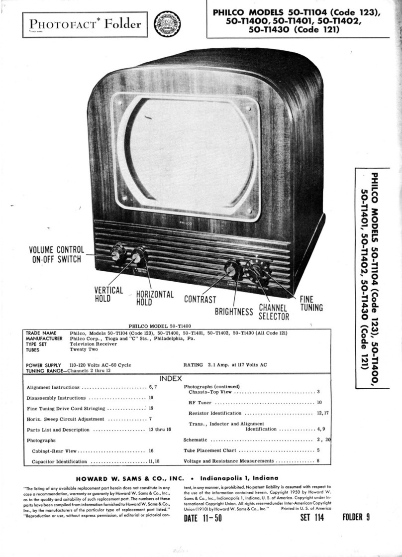
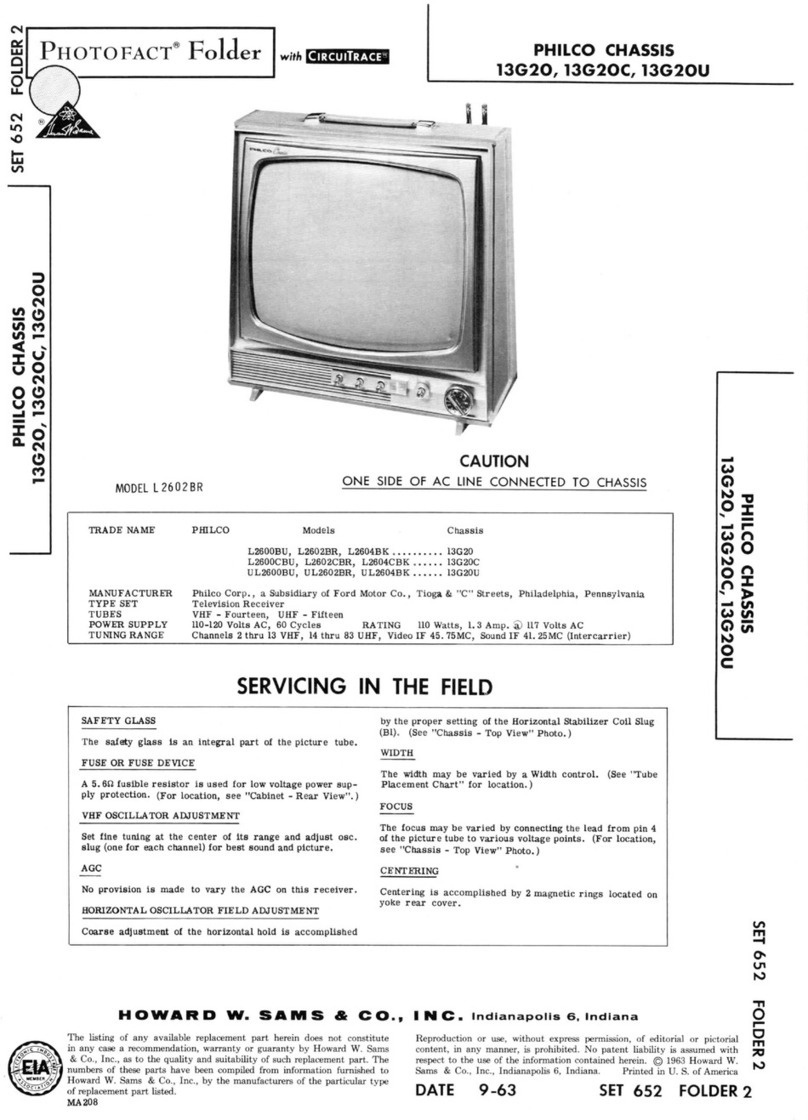
Philco 50-T1443 User manual

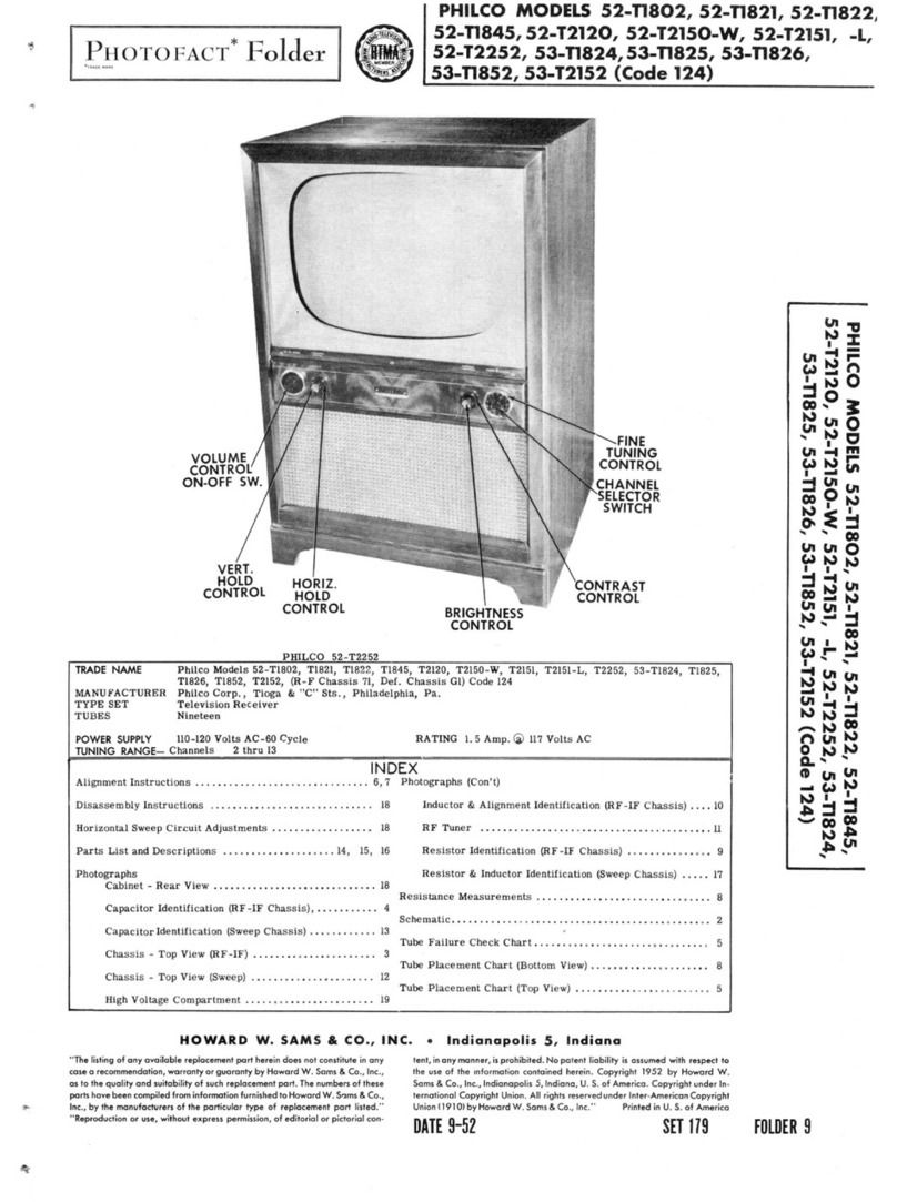
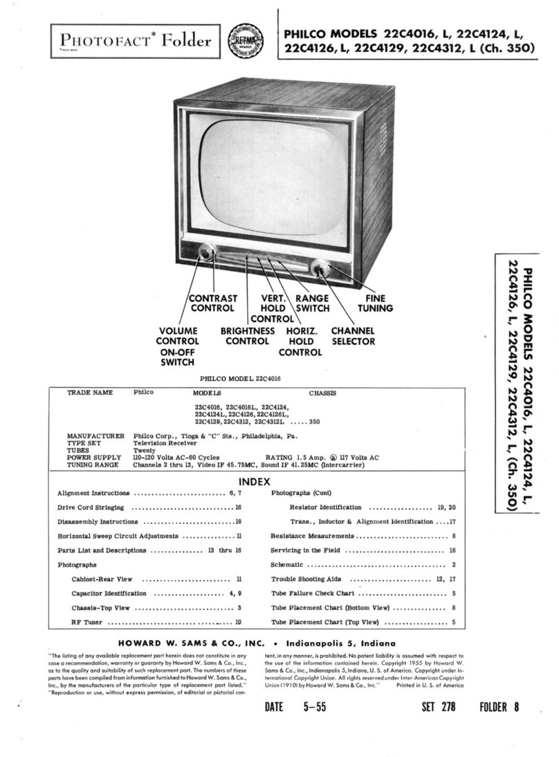
PHOTOFACT*
Folder
PHILCO
MODEL
50-T1443
(CODES
122,123)
HGRIZ.
HOLD
CONT.
VERT.
HOLD
CONT.
V
YWSS
Uis
VOLUMECONT.
ON-OFF
SWITCH
CHANNEL
SEL.
FINE
TUNING
BRIGHT
CONT.
CONTRAST
CONT.
PHILCO
MODEL50-T1443(Code
123)
TRADE
NAME
PhilcoModel50-T1443(Codes
122,
MANUFACTURER
Philco
Corp.
,
Tioga
and
"C"
Sts.
,
TYPE
SET
Television
Receiver
TUBES
Twenty
Six
POWERSUPPLY
110-120
VoltsAC-60Cycle
TUNING
RANGE-Channels
2
thru
13
Photographs
Chassis-Top
View
6,7
20
19
19
13,14
19
11,18
3
123)
Philadelphia,
Pa.
RATING
2
Amp.
® 117
Volts
AC
INDEX
Photographs(continued)
RF
Tuner
10
Resistor
Identification
12,
17
Trans.
,
Inductor
and
Alignment
,15,16
Schematic(AlternateTuner)
16
Voltage
and
Resistance
Measurements
8
o
o
in
O
is
CO
5
•
•
iS
0°
a
m
(/I
to
to
to
CJ
HOWARD
W.
SAMS
&
CO.,
INC.
•
Indianapolis
1,
Indiana
"Thelisting
ofany
available
replacementparthereindoes
not
constitute
inany
case
a
recommendation,warranty
or
guaranty
by
Howard
W.
Sams
&
Co.,Inc.,
as
to the
quality
and
suitability
of
such
replacement
part.
The
numbers
of
these
parts
havebeencompiledfrominformationfurnished
to
Howard
W.
Sams
&
Co.,
Inc.,
bythe
manufacturers
ofthe
particulartype
of
replacementpart
listed."
"Reproduction
or
use,without
express
permission,
of
editorial
or
pictorial
con-
tent,
inany
manner,
is
prohibited.
No
patent
liability
is
assumed
with
respect
to
the
useofthe
informationcontainedherein.Copyright
1950
by
Howard
W.
Sams
&
Co.,Inc.,Indianapolis
1,
Indiana,
U.S.of
America.Copyrightunder
In-
ternationalCopyrightUnion.
All
rights
reserved
under
Inter-American
Copyright
Union(l910)
by
HowardW.Sams&Co.,
Inc."
Printed
inU.S.of
America
DATE
5-50
SET
94
FOLDER
/
®
®i
A
PHOTOFACTSTANDARD
NOTATION
SCHEMATIC
©Howard
W.
Sams
&
Co.,Inc.
1950
PAGE
2

SOUND
IF
AMP
6BA6
®6K

AUDIO
OUTPUT
BLUE
W4GT
94-7

PHILCO
MODEL
5O-T1443
(CODES
122,
123)
/VGIA
dOl
SISSVHO
n
Ul
I

CHASSIS
BOTTOM
VIEW-TRANS.,
INDUC
PAGE
4

U-
TORAND
ALIGNMENT
IDENTIFICATION
PAGE
9

PHILCO
MODEL
5O-T1443
(CODES
122,
123)
1HVHO

ALIGNMENTINSTRUCTIONS
To
eliminate
the
high
voltage
shockhazardremove
the
horizontal
oscillator
tube (V19)
from
its
socket
and
disconnect
the
lead
connectedbetween
pin
3
ofthe
horizontal
output
tube(V20)
andthe
TELEVISION-PHONO
switch.Thiswill
place
the
100J2
resistor
(R126)
inthe
cathodecircuit
to
provide
bias
for
V20and
reduce
the
placecurrent
to
normal.
Do
not
attempt
to
operate
theset
without
the
focus
and
deflection
coils
connected.
Pre-set
the
following
adjustments:
A10
fully
counter-clockwise.
All
andA12
fully
clockwise
.
A8
A3andA7
until
thetopofthe
screws
are
approximately
5/8
inch
from
thetopofthe
coilmount.
Remove
the
converter
tube
(V2)
.
IfV2isa
6J6
replace
it
with
a 6J6
which
haspin1
removed,
ifV2
is
a 7F8
replace
it
with
a 7F8
which
has
pm
6
removed.Thiswilldisable
the
local
oscillator
and
preventerroneousindications.
During
video
IF
alignmentattenuate
signal
generator
to
maintain
2
volt
deflection
on
VTVM.
Turn
the
contrast
control
to
maximumcounter-clockwise.
DUMMY
ANTENNA
.
01MFD
.
01MFD
.
01MFD
.01MFD
.01MFD
Direct
Direct
Direct
SIGNAL
GENERATOR
COUPLING
High
side
topin1
(Grid)
of
6AG5
(V6).
Low
side
to
chassis.
High
side
topin1
(Grid)
of
6AG5
(V5).
Low
side
to
chassis.
High
side
topin1
(Grid)
of
6AG5
(V4).
Low
side
to
chassis.
High
side
topin1
(Grid)
of
6AG5
(V3)
.
Low
side
to
chassis.
High
side
toan
unground-
ed
tube shield
floating
overconvertertube
(V2)
Low
side
to
chassis.
SIGNAL
GENERATOR
FREQUENCY
25.
SMC
(Unmod.)
24.
SMC
(Unmod.)
25MC
(Unmod.)
26.6MC
(Unmod.)
23.25MC
(Unmod.)
28.
IMC
(Unmod.)
22.
IMC
(Unmod.)
24.25MC
(Unmod.)
CHANNEL
Any
"
CONNECT
VTVM
DC
Probe
to
PoinU^\n
to
chassis.
»
ADJUST
Al
A2
A3
A4
A5
A6
A7,A8
A9
REMARKS
Adjust
for
maximumdeflection.
Usethe
peak
with
the
slug
farthestout.
"
"
!•
Adjust
for
MINIMUM
deflection.
Adjust
A7for
MINIMUM
deflection.
If
nodipcanbe
found
adjust
A7
counter-clockwise
until
a
sharp
increase
is
noted,
thenclockwise
tothe
pointjust
before
the
increase
began.
Then
adjust
A8for
minimum
deflection.
Adjust
for
maximumdeflection.
OVERA
L
VIDEO
IF
RESPONSECHECK
Connect
the
synchronizedsweepvoltage
from
the
signalgenera
Connect
a
lOKft
resistor
in
series
with
the
oscilloscope
vertica
DUMMY
ANTENNA
Direct
SWEEP
GENERATOR
COUPLING
High
side
toanun-
grounded
tubeshield
floating
overconverter
tube
(V2)
.
Low
side
to
chassis.
SWEEP
GENERATOR
FREQUENCY
25MC
(10MC
SWP)
MARKER
GENERATOR
FREQUENCY
23.
2
SMC
23.
SMC
25.75MC
26.6MC
tortothe
horizontal
input
ofthe
oscilloscope
ofor
horizontal
deflection,
input.
CHANNEL
Any
CONNECT
SCOPE
Vert.
Amp.
to
Point
^O.
Low
side
to
cnassis.
ADJUST
A10
REMARKS
Adjust
AlO
for
responsecurvewithin
the
limits
shown
inFig1.If
necessary
retouch
Al,A2,A3,A4,
A5,
A9andAlO
for
properresponse.
SOUND
IF
ALIGNMENT
Connect
the
synchronizedsweepvoltage
from
the
signalgenerator
tothe
horizontal
input
ofthe
oscilloscope
for
horizontaldeflection.
Attenuate
the
sweepgenerator
to
maintain
.5
volt peak
to
peakindication.
DUMMY
ANTENNA
Direct
Direct
Direct
DUMMY
ANTENNA
.01MFD
SWEEP
GENERATOR
COUPLING
High
side
toanun-
grounded
tubeshield
floating
overconverter
tube
(V2)
.
Low
side
to
chassis
.
"
SWEEP
GENERATOR
COUPLING
High
side
to
Point
A .
Low
side
to
chassis.
SWEEP
GENERATOR
FREQUENCY
22.
IMC
(IMC
SWP)
"
SWEEP
GENERATOR
FREQUENCY
Not
used
MARKER
GENERATOR
FREQUENCY
22.
IMC
(400
% AM
Mod.)
"
22.
IMC
(Unmod.)
4.5M
MARKER
GENERATOR
FREQUENCY
4.
SMC
(400
t
AM
Mod.)
CHANNEL
Any
"
•'
TRAP
ADJ
CHANNEL
Any
CONNECT
SCOPE
Vert.Amp.
to
Point
X*/-
Low
side
to
cnassis.
"
JSTMENT
CONNECT
SCOPE
Vert.Amp.
topin
2
of
picturetube.
ADJUST
All,
A12
A13.A14
All,
A12
ADJUST
A15
REMARKS
Adjust
AllandA12
slightlyclockwiseuntil
an
indication
is
observed
onthe
scope.
Adjust
A13for
minimum
AM
indication
.
Adjust
A14
for
symmetrical
"S"
curve
similar
toFig2.
Adjust
for
maximumamplitude
and
symmetry
of
pattern.
REMARKS
Adjust
for
minimum
400
^
indication
on
scope.
3.
4.
FIG.2
FIG.3
FIG.4
PAGE
6

OSCILLATOR
ALIGNMENT
(TUNER
76-5411-3)
Connect
two
matched
lOOKfi
(
-
1%)
resistors
in
series
from
point
A to
chassis.
The
junction
of
these
two
resistors
is
alignment
point<6\.s
shown
on
the
schematic.
"
Complete
oscillator
alignment
maynotbe
necessary.
If
the
oscillator
seem
tobeoff
frequency
approximately
the
same
amount
fora
majority
ofthe
channels,
itmaybe
possible
to
correct
them
inone
step
using
A16.
It
should
be
notedthat
this
is an
all
channel
oscillator
circuitadjustment
and
should
not be
adjusted
for any
individualchannel.
If
adjustment
of A16
will
not
bring
all
channels
within
the
range
ofthe
fine
tuning
control,
it
will
be
necessary
to
adjust
the
individual
channel
oscillator
adjustment
for
each
channel
that
is
off
frequency.
The
individualchannel
oscillator
adjustment
screws
are
reachedthru
a
holejust
tothe
right
ofthe
channelswitchshaft.
The
correct
adjustmentscrew
is
accessible
thru
this
hole
asthe
channelswitch
is
turned
to
eachchannel.
Remove
the
dummy
convertertube
and
replace
the
originaltube.
The
sweep
generator
output
lead
should
be
terminated
with
its
characteristic
impedance,
usually
50
ohms.
Setthe
fine
tuning
control
tothe
mid-position
ofits
range.
DUMMY
ANTENNA
Two
120S2
carbon
res.
SIGNAL
GENERATOR
COUPLING
Across
antennatermin-
als
with
120O
in
each
lead.
SIGNAL
GENERATOR
FREQUENCY
215.75MC
(Unmod.)
209.75MC
(Unmod.)
293.75MC
(Unmod.)
197.75MC
(Unmod.)
191.75MC
(Unmod.)
185.75MC
(Unmod.)
179.75MC
(Unmod.)
87.75MC
(Unmod.)
81.75MC
(Unmod.)
71.75MC
(Unmod.)
65.75MC
(Unmod.)
59.
7
SMC
(Unmod.)
CHANNEL
13
12
11
10
9
8
7
6
5
4
3
2
CONNECT
VTVM
DC
Probe
to
Point/b}
Common
to
Point<v*>
ADJUST
A17
A18
A19
A20
A21
A22
A23
A24
A25
A26
A27
A28
REMARKS
Adjust
for
zero
reading.
A
positive
and
negative
reading
will
be
obtained
on
either
side
ofthe
correct
setting.
RF
ALIGNMENT
(
TUNER
76-5411-3)
The
sweepgenerator
output
leadshould
be
termnated
with
its
characteristic
impedance,usually
50
ohms.
Connect
the
synchronizedsweepvoltage
from
the
signalgenerator
tothe
horizontal
input
ofthe
oscilloscope
for
horizontaldeflection.
DUMMY
ANTENNA
Two
120ft
carbon
res.
SWEEP
GENERATOR
COUPLING
Across
antennatermin-
als
with
120SJ
in
each
lead.
SWEEP
GENERATOR
FREQUENCY
207MC
(10MC
SWP)
213MC
(10MC
SWP)
201MC
(10MC
SWP)
195MC
(10MC
SWP)
189MC
(10MC
SWP)
183MC
(10MC
SWP)
177MC
(10MC
SWP)
85MC
(10MC
SWP)
79MC
(10MC
SWP)
69MC
(10MC
SWP)
63MC
(10MC
SWP)
57MC
(10MC
SWP)
MARKER
GENERATOR
FREQUENCY
205.25MC
209.75MC
211.
2
SMC
215.75MC
199.25MC
203.
7
SMC
193.25MC
197.75MC
187.25MC
191.75MC
181.25MC
185.75MC
175.25MC
79.75MC
83.25MC
87.75MC
77.
2
SMC
81.75MC
67.25MC
.71.75MC
61.
2
SMC
65.75MC
55.25MC
59.75MC
CHANNEL
12
13
11
10
9
8
7
6
5
4
3
2
CONNECT
SCOPE
Vert.
Amp.
to
Point
<m
Low
side
to
cnassis.
ADJUST
A29,
A30,
A31
REMARKS
Adjust
for
response
curve
similar
to
Fig
3
with
markers
above90%.check
all
channels
for
response
similar
toFig3.
If
markers
fallbelow
70%onany
channel
,
make
slight
adjustment
of
A29,
A30and
A31
withchannelswitch
setfor
thatchannel.
Recheck
all
channels
tosee
thattheyhave
not
beenseriously
effected.
OSCILLATOR
ALIGNMENT
(TUNER
76-4402-5)
Remove
the
dummy
convertertube
and
replace
the
original
tube.
The
sweepgenerator
output
leadshould
be
terminated
with
its
characteristic
impedance,
usually
50
ohms.
Setthe
fine
tuning
control
tothe
mid-position
ofits
range.
DUMMY
ANTENNA
Two
120S2
carbon
res.
SIGNAL
GENERATOR
COUPLING
Across
antenna
termin-
als
with
120ft
in
each
lead.
SIGNAL
GENERATOR
FREQUENCY
59.
7
SMC
(Unmod)
65.75MC
(Unmod)
71.
7
SMC
(Unmod.)
81.75MC
(Unmod)
87.
7
SMC
(Unmod)
179.75MC
(Unmod)
185.75MC
(Unmod)
191.
75MC
Unmod)
197.75MC
(Unmod)
203.75MC
(Unmod)
209.75MC
(Unmod.)
215.75MC
(Unmod.)
CHANNEL
2
3
4
5
6
7
8
9
10
11
12
13
CONNECT
VTVM
DC
Probe
to
point<0?>
Common
to
chassis.
ADJUST
A32
A33
A34
ASS
A36
A37
A38
A39
A40
A41
A42
A43
REMARKS
Adjust
for
zero
reading.
A
positive
and
negative
reading
will
be
obtained
on
either
side
ofthe
correct
setting.
RF
ALIGNMENT
(TUNER
76-4402-5)
Push
a
piece
of
solder
into
the
holeadjacent
to A9 so
that
the
terminal
under
the
hole
is
shorted
to
chassis.
The
sweep
generator
outputleadshould
be
terminatedwith
its
characteristic
impedance,
usually
50
ohms.
Connect
the
synchronizedsweep
voltage
from
the
signal
generator
tothe
horizontalinput
ofthe
oscilloscope
for
horizontaldeflection.
DUMMY
ANTENNA
Two
120ft
carbon
res.
••
SWEEP
GENERATOR
COUPLING
Across
antenna
termin-
als
with
120ft
in
each
ead.
SWEEP
GENERATOR
FREQUENCY
57MC
(10MC
SWP)
8SMC
(10MC
SWP)
213MC
(10MC
SWP
MARKER
GENERATOR
FREQUENCY
54MC
60MC
82MC
88MC
210MC
216MC
CHANNEL
2
6
13
CONNECT
SCOPE
€
..
Amp.
to
Point
Low
side
to
sis.
••
••
ADJUST
A44
A45
A46.A47
REMARKS
Adjust
for
response
curve
similar
to
Fig4
with
markers
at
70%.
Adjust
for
maximumamplitude
and
symmetry.
PAGE
7
o
o
m
r-
in
*x
§i
z
KJ
io

•o
S
VOLTAGE
AND
RESISTANCE
MEASUREMENTS
VOLTAGEREADINGS
RESISTANCE
READINGS
Item
V
1
V2
V
3
V
4
V
5
V
6
V7
V
8
V9
V
10
V
1 1
V
12
V13
V
14
V
15
V16
V
17
V
18
V
19
V20
V21
V22
V23
V24
V25
V26
Tube
6BC5
6J6
6BC5
6BC5
6BC5
6BC5
6AL5
6ATJ6
7C5
7F7
6BA6
6AU6
6AL5
6AU6
6K6GT
7N7
7N7
6K6GT
7N7
6BG6G
6W4GT
1B3GT
1B3GT
5U4G
7Z4
12LP4
Pin1
-.4VDC
95VDC
-2.
5VDC
-2.
1VDC
-.4VDC
0V.
0V.
0V.
0V.
6.
3VAC
0V.
-.4VDC
-4.2VDC
-.4VDC
0V.
6.
3VAC
6.
3VAC
6.
3VAC
6.
3VAC
0V.
OV.
Pin
2
0V.
120VDC
.6VDC
.9VDC
.4VDC
1.
2VDC
-2.8VDC
0V.
340VDC
5.4VDC
0V.
0V:
-.3VDC
0V.
6.
3
VAC
0V.
5.4VDC
0V.
-12VDC
6.
3VAC
0V.
Pin
3
6.
3
VAC
ov.
ov.
ov.
ov.
ov.
ov.
6.
3VAC
125VDC
160VDC
OV.
OV.
6.
3VAC
OV.
275VDC
160VDC
340VDC
340VDC
44VDC
OV.
430VDC
Pin
4
OV.
6.
3VAC
6.
3VAC
6.
3VAC
6.
3VAC
6.3VAC
6.
3VAC
OV.
-3VDC
5.
4VDC
6.
3
VAC
6.
3VAC
OV.
6.
3VAC
295VDC
-1VDC
-75VDC
340VDC
-9VDC
-20VDC
OV.
Pin
5
165VDC
-1.
6VDC
150VDC
150VDC
150VDC
100VDC
.1VDC
250VDC
OV.
ov.
120VDC
65VDC
OV.
220VDC
OV.
-.7VDC
-75VDC
OV.
-55VDC
-20VDC
360VDC
Pin
6
165VDC
§-6.8VDC
150VDC
150VDC
150VDC
140VDC
OV.
140VDC
-1VDC
OV.
120VDC
65VDC
OV.
44VDC
295VDC
33VDC
80VDC
260VDC
6.3VAC
Pin
7
OV.
OV.
.6VDC
.9VDC
.4VDC
1.
2VDC
-1.
5VDC
1
VDC
9VDC
1.2VDC
1.
3VDC
OV.
-2.9VDC
OV.
OV.
OV.
OV.
6.3VAC
155VDC
|
OV.
335VDC
!ov.
ov.
1
ov.
Pin
8
8.3VAC
OV.
20
VDC
OV.
OV.
24
VDC
51VDC
OV.
240VDC
280VDC
6.
3VAC
Pin
9
TOPCAP
*
*DONOT
MEASURE.
»
DONOT
MEASURE.
0V.
6.3VAC
6.
3
VAC
390VDC
0V.
.4VDC
OV.'
210VAC
PIN10
275VDC
330VAC
OV.
PIN11
145VDC
OV.
OV.
PIN12
OV.
330VAC
210VAC
OV.
200VDC
390VDC
OV.
i
TAKENWITHVACUUM
*DONOT
MEASURE.
TUBE
VOLTMETER.
Item
V1
V
2
V
3
V
4
V
5
V
6
V
7
V
8
V9
V
10
V1 1
V
12
V
13
V14
V15
V
16
V
17
V18
V
1 9
V20
V
21
V22
V23
V24
V25
V
26
Tube
6BC5
6J6
6BC5
6BC5
6BC5
6BC5
6AL5
6AU6
7C5
7F7
6BA6
6AU6
6AL5
6AU6
6K6GT
7N7
7N7
6K6GT
7N7
6BG6G
6W4GT
1B3GT
1B3GT
5U4G
7Z4
12LP4
Pin1
200KSZ
TSKn
leoKn
165KSJ
165KS2
.2£l
.2n
IMeg.
on
.in
470KSJ
68Kfi
Inf.
4.
7
Meg.
Inf.
JB
.in
.in
.in
Inf.
Inf.
Inf.
Inf.
Inf.
.in
an
Pin
2
on
tiOKn
6sn
i2on
68n
loon
120KS1
on
#3.
5M
woon
on
on
Inf.
on
JO
on
1.
2Kn
on
290Kn
.in
Inf.
Inf.
Inf.
12.
5Kn
Inf.
1.5
Meg.
Pin
3
.in
on
on
on
on
on
on
.in
»20Kn
#47Kn
on
on
.in
on
|2.6Kn
#15.4Kn
*ioOKn
#1.
2Kn
*42Kn
on
*
on
Inf.
Inf.
Inf.
4on
PIN10
*5Kn
Pin
4
on
.in
.in
.in
.in
.in
an
on
38Kn
IMeg.
an
an
on
an
#2.iKn
56DKn
2
Meg.
#1.
2Kn
750Kn
350Kn
Inf.
Inf.
Inf.
52H
Inf.
PIN11
lOOKn
Pin
5
|2.6Kn
225Kn
t825n
t4son
t48on
t7Kn
8Kn
*i3Kn
Inf.
on
ti.
sxn
tiucn
on
*49Kn
IMeg.
4.7
Meg.
2
Meg.
2.
2
Meg.
IBOKn
350Kn
M30n
Inf.
Inf.
Inf.
_,
Inf.
PIN
12
on
Pin
6
t2.6Kn
losn
t82sn
t4son
t4son
ti.
5Kn
Inf.
tioxn
ssoxn
on
ti.
8Kn
nucn
Inf.
#560Kn
K.iKn
«8Kn
i
sooKn
i
3
Mez.
an
#80Kn
550Kn
Inf.
Inf.
Inf.
52n
4on
Pin
7
on
on
esn
I2on
esn
won
3
soon
I2on
issn
IMeg.
68P,
on
46Kn
on
on
on
on
an
on
on
on
Inf.
Inf.
Inf.
24Kn
Pin
8
an
on
seon
on
on
eooon
looon
on
#4.5Kn
#iOKn
an
Inf.
Inf.
12.
5Kn
on
ALL
MEASUREMENTSTAKENWITH
TV-PHONO
SWITCH
IN
"TV"
POSITION,
t
MEASURED
FROM
PIN7 OF
V25.
»
MEASURED
FROM
PIN8 OF
V24.
i
MEASURED
FROM
PIN3 OF
V21.
Pin
9
TOPCAP
iiion
TOPCAP
•
soon
TOPCAP
A
Inf.
1.
DC
Voltage
measurements
areat
20,000
ohms
per
volt;
AC
Voltage
measured
at
1,000
ohms.
2.Pin
numbers
are
counted
ina
clockwise
direc-
tion
on
bottom
of
socket.
3.
Measured
values
ore
from
socket
pinto
com-
mon
negative
unless
otherwise
stated.
4.
Line
voltage
maintained
at
117
volts
for
volt-
age
readings,
5.
Front
panels
controls
set
at
minimum.
6.
Where
readings
may
varyaccording
to
the
setting
ofthe
service
Controls,
both
minimum
and
maximum
readingsare
given.

RF
TUNER-RIGHT
SIDE
RF
TUNER-LEFT
SIDE
PAGE
1O

CHASSIS
BOTTOM
VIEW-CAF
PAGE
18

>ACITOR
IDENTIFICATION
PAGE
11

CHASSIS
BOTTOM
VIEW-RES
PAGE
12

BISTOR
IDENTIFICATION
PAGE
17

PARTSLIST
AND
DESCRIPTIONS
TUBES
(SYLVANIA
or
Equivalent)
ITEM
No.
VIA
B
V2A
B
V3A
B
V4A
B
V5A
B
V6A
B
V7
V8
V9
V10
Vll
V12
V13
V14
V15
V16
V17
V18
V19
V20
V21
V22
V23
V24
V25
V26
USE
RF
Amp.
RF
Amp.
Converter
Converter
1st
Video
IF
1st
Video
IF
2nd
Video
IF
2nd
Video
IF
3rd
Video
IF
3rd
Video
IF
4th
Video
IF
4th
Video
IF
Video
Del.
-AGC
Rect.
Video
Amp.
VideoOutput
DC
Rest.
-Sync.
Amp.
1st
Sound
IF
2nd
Sound
IF
Ratio
Det.
AF
Amp.
Audio
Output
Sync.
Amp.
-Sync.
Sep.
Vert.
Osc.-Vert.
Dlsch.
Vert.
Output
Hor.
AFC
-Hor.
Oscillator
'*
Hor
.
Output
Damper
HV
Rect.
HV
Rect.
LV
Rect.
LV
Rect.
Picture
Tube
REPLACEMENT
DATA
PH1LCO
PART
No.
6BC5
BAG
5
616
7F8
6BC5
6AG5
6BC5
6AG5
6BC5
6
AC
5
SBC
5
6AG5
6AL5
6AU6
7C5
7F7
6BA6
6AU6
6AL5
6AU6
6K6GT
7N7
7N7
6K6GT
7N7
6BG6G
6W4GT
1B3GT
1B3GT
5U4G
7Z4
12LP4
STANDARD
REPLACEMENT
6BC5
6AG5
6J6
7F8
6BC5
6AG5
6BC5
6AG5
6BC5
6AG5
6BC5
6AG5
6AL5
6AU6
7C5
7F7
6BA6
6AU6
6AL5
6AU6
6K6GT
7N7
7N7
6K6GT
7N7
6BG6G
6W4GT
1B3GT
1B3GT
5U4G
7Z4
12LP4
RMA
BASE
TYPE
7BD
7BD
7BF
8BW
7BD
7BD
7BD
7BD
7BD
7BD
7BD
7BD
6BT
7BK
6AA
8AC
7BK
7BK
6BT
7BK
7S
SAC
8AC
7S
8AC
5BT
4CG
3C
3C
5T
SAB
12D
NOTES
Used
in
code
0123
Used
in
code#122
Used
in
code
#123
Used
in
code
#122
Used
in
code
#123
Used
in
code
#122
Used
in
code
1123
Used
in
code
#122
Used
in
code
#123
Used
in
code
#122
Used
in
code
#123
Used
in
code#122
CAPACITORS
Capacity
values
given
inthe
rating
column
arein
mfd.
(or
Electrolytic
and
Paper
Capacitors,
andin
mmfd.
for
Mica
and
CeramicCapacitors.
ITEM
No.
Cl
C2A
B
C
D
C3
C4A
B
C
C5A
B
C6A
B
C
D
C7A
B
C
C8
C9
CIO
Cll
C12
C13
C14
CIS
C16A
B
C17
CIS
C19
C20
C21
C22
C23
C24
C25
C26
C27
C28
C29
C30
C31
C32
C33
C34
C35
C36
C37
C38
C39
C40
C41
C42
C43
C44
C45
C46
RATING
CAP.
30
40
20
10
10
30
10
10
40
10
40
10
10
10
10
10
10
10
10
2
5
120
1000
100
20
10
1000
1000
10
1000
100
120
51
51
1500
1503
1500
1500
470
1503
10
470
1500
1500
10
470
51
51
1503
1500
470
100
1500
1500
100
100
10
.047
VOLT
475
475
475
475
475
250
450
450
50
450
50
475
475
475
475
475
475
475
25
50
300
400
REPLACEMENT
DATA
PHILCO
PART
No.
30-2568-19
30-2570-8
30-2568-19
30-2579-16
30-2570-16
30-2570-10
30-2570-10
30-2417-1
30-2417-7
30-1224-5
60-10125237
45-3505-52
62-215001011
60-00205307
62-010009001
45-3505-52
45-3505-52
62-010009001
45-3505-52
62-21500101
60-10125237
30-1224-2
30-1224-2
62-215001011
62-215001311
62-215001011
62-215001011
62-147301001
62-215301011
62-010009001
62-147001001
62-215001011
62-215001011
62-010009001
62-147001001
30-1224-2
30-1224-2
62-215001011
62-215001011
62-147001001
62-110009001
62-215001011
62-215001011
62-110009001
62-110009001
62-010009001
45-3505-28
AEROVOX
PART
No.
AF6X
AF8422J
AF6F
[-AF22J
LpRS
50/50
rAF22J
LPRS
so/so
AF2222X
AFH2222X
E26A274
E26K6
SI5CNPO
GP120M
GP1000M
GP100M
SI20JNPO
SI10JN750
GP1000M
GP1000M
CN10JNPO
GP1000M
GP100M
GP120K
SI51JN220
SI51JN220
GP1500M
GP1500M
GP1500M
GP1500M
GP470M
GP1500M
GP10K
GP470M
GP1500M
GP1500M
GP10K
GP1500M
SI51JN220
SI51JN220
GP1500M
GP1500M
GP470M
GP100M
GP1500M
GP1500M
GP100M
GP100M
GP10K
P488-047
CENTRALAB
PART
No.
D2-4.7
D6-121
D6-102
D6-101
D2-20
DN-10
D6-102
D6-102
D2-10
D6-102
D6-101
D6-121
D2-51
D2-51
D6-152
D6-152
D6-152
D6-152
D6-471
D6-152
D6-100
D6-471
D6-152
D6-152
D6-100
D6-471
D2-51
D2-51
D6-152
D6-152
D6-471
D6-101
D6-152
D6-152
D6-101
D6-101
D6-100
ERIE
PART
No.
NPOK-5
GP2K-120
GP2L-001
GP1K-100
NPOK-20
N750K-10
GP2L-001
GP2L-001
NPOK-10
GP2L-001
GP1K-100
GP2K-120
NPOM-50
NPOM-50
GP2L-0015
GP2L-0015
GP2L-0015
GP2L-0015
GP2K-470
GP2L-0015
GP1K-10
GP2K-470
GP2L-0015
GP2L-0015
GP1K-10
GP2K-470
NPOM-50
NPOM-50
GP2L-0015
GP2L-0015
GP2K-470
GP1K-100
GP2L-0015
GP2L-0015
GP1K-100
GPIK^IOO
GP1K-10
SPRAGUE
PART
No.
TVL-7
TVL-40
TVL-63
TVL-52
TVL-52
TVL-39
TVL-39
TVA-5
TVA-12
\
29C7
29C4
MS
-45
MS-45
1FM-215
1FM-215
1FM-215
1FM-215
1FM-35
1FM-215
MS
-41
1FM-35
1FM-215
1FM-215
MS
-41
1FM-35
MS-45
MS-45
1FM-215
1FM-215
1FM-35
1FM-31
1FM-215
1FM-215
1FM-31
1FM-31
MS
-41
TM-15
IDENTIFICATION
CODES
AND
INSTALLATION
NOTES
Filter
.
Filter
•
Filter
i
Filter
Filter
Filter
•
Decoupling
A
Decoupling
Output
Cathode
Bypass
•
Vert.
Osc.
Decoupling
Vert.
OutputCath.
Bypass
•
Vert.
Osc.
Plate
Decoup.
•
Sync.
Amp.
Plate
Decoup.
*
Decoupling
Decoupling
.
V.
Output
Screen
Bypass
A
V.
Output
Plate
Decoup.
Decoupling
AGC
Filter
Stabilizing
Cap.
Fixed
Trimmer
*
RF
Decoupling
RF
Filament
Bypass
RF
Coupling
Osc.
Grid
Cap.
Fixed
Trimmer
RF
Bypass
Conv.
Filament
Bypass
Fixed
Trimmer
Conv.
Plate
Decoupling
*
Filament
Bypass
*
IF
Coupling
Fixed
Trimmer
Fixed
Trimmer
AGC
Filter
AGC
Filter
RF
Bypass
1stV.IF
Decoupling
IF
Coupling
2nd
V.IF
Decoupling
2nd
V. IF
Decoupling
IF
Coupling
AGC
Filter
3rd
V.IF
Decoupling
3rdV.IF
Decoupling
IF
Coupling
Fixed
Trimmer
Fixed
Trimmer
4th
V.IFCath.
Bypass
4th
V.IF
Decoupling
IF
Coupling
IF
Coupling
DAGC
Decoupling
AGC
Filter
AGC
Filter
Bias
Filter
V.
Diode
Filter
VideoCoupling
i
o
p
01
si
O
0?
Jo
KJ
w
CJ
PAGE
13

CAPACITORS
CCONT.J
PARTS
LIST
AND
DES<
RESISTOR.
ITEM
No.
C47
C48
C49
C50
C51
C52
C53
C54
C55
C56
C57
C58
C59
C60
C61
C62
C63
C64
C65
C66
C67
C68
C69
C70
C71
C72
C73
C74
C75
C76
C77
C78
C79
C80
C81
C82
C83
C84
C85
C86
C87
C88
C89
C90
C91
C92
C93
C94
C95
C96
C97
C98
C99
C100
C101
C102
C103
C104
CIO
5
C106
RATING
CAP.
680
470
56
.1
.047
.0047
56
.01
470
1500
56
1500
1500
1500
100
1500
100
.01
100
.0022
.01
.1
.01
.0068
.047
330
22
.047
220
.082
.0022
.0047
.0047
.0022
.0047
.047
.068
.1
150
180
.0022
.022
.22
5
.047
270
1500
390
.047
.047
.047
.47
500
500
500
.47
.1
.01
.01
470
VOLT
400
400
600
100
400
400
400
400
600
1000
400
500
500
400
500
400
600
600
600
600
600
400
400
400
500
500
600
400
400
500
400
500
500
500
400
400
400
200
20000
20000
20000
200
200
600
600
REPLACEMENT
DATA
PHILCO
PART
No.
60-10685401
62-147001001
62-056409001
45-3505-47
45-3505-28
45-3505-56
62-056409001
45-3505-41
62-147001001
62-215001011
62-056409001
62-215001001
62-215001001
62-215001001
62-110009001
62-215001001
62-110009001
45-3505-41
62-110009001
45-3505-54
45-3505-41
45-3505-47
45-3505-41
45-3505-57
45-3505-45
60-10335407
62-322009001
61-0122
62-122001001
30-4651-3
45-3505-54
45-3505-56
45-3505-56
45-3505-54
45-3505-56
45-3505-62
45-3501
45-3505-47
60-10155407
30-1220-30
45-3505-54
61-0108
45-3505-49
60-90505007
45-3505-45
60-10275407
60-20155014
60-10395407
45-3505-62
45-3505-62
45-3505-62
61-0133
30-1229-2
30-1229-2
30-1229-2
61-0137
45-3505-30
45-3505-41
45-3505-41
62-147001001
AEROVOX
PAST
No.
GP680M
GP470M
GP51K
P488-1
P488-047
P688-0047
GP51K
P488-01
GP470M
GP1500M
GP51K
GP1500M
GP1500M
GP1500M
GP100M
GP1500M
GP100M
P488-01
GP100M
P488-0022
P488-01
P488-1
P688-01
P1088-0068
P488-047
1468-00035
1468-000025
P488-047
1468-00025
P488-075
P688-0022
P688-0047
P688-0047
P688-0022
P688-0047
P488-047
P488-068
P488-1
1469-00015
1469-00015
P688-0022
P488-022
P488-22
1468-000005
P488-047
1469-00025
1464-0015
1468-0004
P488-047
P488-047
P488-047
P288-47
P288-47
P288-1
P688-01
P688-01
GP470M
CENTRALAB
PART
No.
D6-681
D6-471
D2-56
D6-472
D6-560
D6-103
D6-471
D6-152
D6-560
D6-152
D6-152
D6-152
D6-101
D6-152
D6-101
D6-103
D6-101
D6-222
D6-103
D6-103
D6-682
B6-3J1
D6-220
D6-221
D6-222
D6-472
D6-472
D6-222
D6-472
D6-151
D6-181
D6-222
D2-4.7
D6-271
D6-152
D6-391
TV1-502
TV1-502
TV1-502
D6-103
D6-103
D6-470
ERIE
PART
No.
GP2K-680
GP2K-470
GP1K-56
GP2M-0047
GP1K-56
821-01
GP2K-470
GP2L-0015
GP1K-56
GP2L-0015
GP2L-0015
GP2L-0015
GP1K-100
GP2L-0015
GP1K-100
821-01
GP1K-100
GP2M-0022
821-01
821-01
GP2K-330
GP1K-22
GP2K-220
GP2M-0022
GP2M-0047
GP2M-0047
GP2M-0022
GP2M-0047
GP2K-150
GP2K-180
GP2M-0022
NPOK-5
GP2K-270
GP2L-0015
GP2K-390
821-01
821-01
GP2K-470
SPRAGUE
PART
No.
1FM-37
1FM-35
MS-45
TM-1
TM-15
TM-25
MS-45
TM-11
1FM-35
1FM-215
1FM-45
1FM-215
1FM-215
1FM-215
1FM-31
1FM-215
1FM-31
TM-11
1FM-31
TM-22
TM-11
TM-1
TM-11
MB-27
TM-15
1FM-335
MS
-425
TM-15
1FM-325
TM-1
TM-22
TM-25
TM-25
TM-22
TM-25
TM-15
TM-1
MS-315
MS-315
TM-22
TM-12
TC-2
MS-55
TM-15
MS-325
1FM-215
1FM-34
TM-15
TM-15
TM-15
TC-5
TC-5
TM-1
TM-E
TM-11
1FM-35
IDENTIFICATION
CODES
AND
INSTALLATION
NOTES
V.
Amp.
Cath.
Bypass
t
Filament
Bypass
Fixed
Trimmer
Video
Coupling
Video
Coupling
Video
Coupling
Fixed
Trimmer
S.IF
Coupling
1st
S
.
IF
Cathode
Bypass
1st
S.
IF
Decoupling
S.
IF
Coupling
RF
Bypass
RF
Bypass
2nd
S.IF
Decoupling
DiodeLoadCap.
RF
Bypass
RF
Bypass
Audio
Coupling
ToneCompensation
ToneCompensation
Audio
Coupling
AF
Amp.
Screen
Bypass
Audio
Coupling
Output
Plate
Bypass
Sync.Coupling
Sync.
Coupling
Sync.Sep.Grid
Bypass
Sync.Coupling
RF
Bypass
2nd
Sync.
Amp.
Cath.
Bypass
Integrator
Net.
Integrator
Net.
Integrator
Net.
Fixed
Trimmer
Vert.Osc.GridCap.
Vert.
Discharge
Vert.
Discharge
Vert.SweepCoupling
Hor.Sync.Coupling
VoltageDivider
Hor.Sync.Coupling
AFC
Filter
AFC
Filter
Hor.Feedback
Hor.
AFC
Plate
Bypass
Hor.Osc.GridCap.
Hor.
Discharge
Hor.SweepCoupling
Hor.Output
Screen
Bypass
Damper
Filter
Damper
Filter
Hor.Sweep
Coupling
VoltageDoublerCap.
HV
Filter
HV
Filter
Pic.TubeCath.
Bypass
Bias
Filter
Line
Filter
Line
Filter
RF
Bypass
*
'
Not
used
inall
models.
t
Model
50-T1443
code
123
before
run
5
uses
.0033MFD
in
this
application.
Part
No.
45-5305-:
CONTROLS
ITEM
No.
R1A
B
C
R2A
B
R3
R4
R5
R6
R7
R8
RATING
RESIST-
ANCE
SOKfi
IMeg.
Shaft
End
2
Meg.
Switch
2000!!
100K!2
lOKtl
5000S1
soon
2.5
Meg.
WATTS
i
a
I
JL
2
i
4
2
25
^
REPLACEMENT
DATA
PHILCO
PART
No.
^
1
(
33-5563-3
{
)
I
33-5564-1
NotReq.
33-5546-33
33-5539-43
33-5546-18
33-5546-10
33-5547-5
33-5565-10
IRC
PART
No.
Bll-123
*
Bll-137
*
E-187
*
Q18-139X
76-1
W-2000
Qll-128
W-5000
PR
-25-500
QU-239
CLAROSTAT
PART
No.
T-116
SW-A
43-2000
M-49-S
10-10K
43-5000
PW-25-500
M-84-S
CENTRALAB
PART
No.
BT-78-S
NotReq.
V-110
B-40
V-135
B-83
INSTALLATION
NOTES
Horiz.
hold control,panel
Vert,
hold
control,
rear
Attach
per
instructions
in
"Concentrikit"
Volume
control,
tapped©
1
Meg.
Attach
toR2Aper
instructions
Contrast
control-Wire
Wound
Brightness
control
Deflection
control-Wire
Wound
Vert,
linearity
control-Wire
Wound
Focus
control-Wire
Wound
Height
control
*
Additonal
parts
tobe
used
with
"Concentrikit"
RESISTORS
ITEM
No.
R9
RIO
Rll
R12
R13
R14
R15
R16
R17
R18
R19
R20
R21
R22
R23
R24
R25
R26
R27
RATING
RESISTANCE
3900!!
47Kt!
10KS1
2200!!
4700!!
220KS1
15K!!
10K!1
10KS!
4700!!
1000!!
5600!i
5%
15K!!
68!!
330H
33001!
20%
3300!!
20%
5600!!
120!!
WATTS
1
\
»
2
I
2
1
2
Z
±
-£
i
~z
~z
L
i
I
i
i-
i
^
REPLACEMENT
DATA
PHILCO
PART
No.
66-2398340
66-3478340
66-3108340
66-2228340
66-2478340
66-4228340
66-3158340
66-3108340
66-3108340
66-2478340
66-2018340
66-2568340
66-3158340
66-0688340
66-1338340
66-2338340
66-2338340
66-2568340
66-1128340
IRC
PART
No.
BTS-3900
BTS-2200
BTS-4700
BTS-4700
BTS-5600-5%
BTS-15K
BW-j-330
BTS-3300
BTS-3300
IDENTIFICATION
CODES
ALL
RESISTORS
ARE±10%
UNLESSOTHERWISE
STATED
.
Ant.CoilShunt
AGC
Network
RF
Plate
CoilShunt
RF
Decoupling
Conv.
Grid
Conv,
Grid
Conv,
Plate
Coil
Shunt
Conv.
Plate
Decoupling
Osc.
Grid
Osc.
Plate
Parasitic
Supp.
-SeeNote
1
IF
Filter
Network
-See
Note
2
1st
Video
IF
Transformer
Shunt
1st
Video
IF
Cathode
1st
Video
IF
Decoupling-wire
Wound
AGC
Network
AGC
Network
2nd
Video
IF
Grid
2nd
Video
IF
Cathode
ITEM
No.
R28
R29
R30
£31
R32
R33
R34
R35
R36
R37
R38
R39
R40
R41
R42
R43
R44
R45
R46
H47
R43
R49
R50
R51
R52
R53
R54
R55
H56
H57
R58
R59
R60
R61
R62
R63
R64
R65
R66
R67
R68
R69
H70
R71
R72
R73
R74
R75
R76
R77
R78
R79
R80
R81
R82
R83
R84
R85
R86
H87
R88
H89
R90
R91
R92
R93
R94
H95
R96
R97
R98
R99
R100
R101
R102
R103
R104
R105
R106
R107
R108
R109
R110
Rill
R112
R113
R114
R115
R116
H117
R118
R119
R120
R121
R122
R123
R124
R125
H126
R127
R128
R129
R130
R131
R132
R133
RATING
RESISTANCE
3300!!
20%
5600H
68SJ
5600
a
5100!!
5%
5K£2
oo
a
5600!!
ooora
27KS2
20KS2
ooon
6800!!
20%
OOOS2
OKI!
3300O
Meg.
2on
OKS1
2700«
5%
470KSJ
20%
10£!
6800!J
68KSJ
2500S2
470!!
5KSJ
OK!!
looon
100KH
20%
27KS!
OKSJ
470KSJ
20%
Meg.
20%
470KQ
20%
Ban
ooon
330S1
68K!2
20%
10KS2
22KSJ
47!!
4.7H
330SJ
47KS2
10KSJ
97KS2
20%
4.7
Meg.
20?
560KS2
47K!!
1
Meg.
20%
560S2
1900!!
330!!
270S1
470K!J
20%
10KSJ
5100B
10KS!
4.7
Meg.
6800!!
33001!
56KJi
IMeg.
4700SJ
1200!!
10KS!
3900!!
33K!2
22KSJ
8200SJ
8200SJ
10KS!
68KS!
1
Meg.
100KS2
lOOKSJ
470KSJ
820K£2
3900SJ
2.2
Meg.
20%
looon
560KSJ
180KIJ
lOOKfl
5%
8200H
3.3
Meg.
5%
82KS1
42KSJ
560KSJ
5%
220KS!
10KS1
10K!!
82KS2
5%
10KSJ
5%
68KS2
5%
100!!
20%
330KS!
won
3900SJ
2
Meg.
47KSJ
12Si
act
220KSJ
20%
18KS2
WATTS
a
i
1
1
I
I
A
a
I
a
1
2
f
T
r
|
|
L
1
|
I
i
5
1
1
2
2
S
2
I
~
a
I
I
I
~a
1
1
f
i
2
f
2
1
1
2
I
z
2
10
1
2
i
2
5
I
I
X
1
2
JL
I
I
4
~
1
?
i
\
\
2
1
1
I
z
1
1
4
i
1
i
1
1
i
1
~
i
\
1
^
\
2
2
i
2
2
2
10
REPLACEMENT
DATA
PHILCO
PART
No.
66-2338340
66-2568340
66-0688340
66-2568340
66-2518240
66-3158340
66-1108340
66-2568340
66-2018340
66-3278340
66-4128340
66-2018340
66-2688340
66-2018340
66-3108340
66-2338340
66-5108340
66-1124340
66-3108340
66-2274340
6-4478340
66-0108340
66-2688340
66-3684340
3-1335-87
66-1474340
66-3154340
66-3105340
66-2104340
66-4108340
66-3278340
66-3108340
66-4478340
66-5108340
66-4478340
66-0688340
66-2108340
66-1338340
66-3688340
66-3108340
66-3228340
66-0478340
66-9478340
66-1338340
66-3478340
66-3108340
66-3478340
66-5478340
66-4568340
66-3474340
66-5108340
66-1564340
33-3435-15
66-1338340
66-1274340
66-4478340
66-3104340
33-1335-18
66-3108340
66-5478340
66-2688340
66-2338340
66-3564340
66-5108340
66-2478340
66-2128340
66-3108340
66-2398340
66-3334340
66-3228340
66-2828340
66-2828340
66-3108340
66-3688340
66-5108340
66-4108340
66-4108340
66-4474340
66-4828340
66-2398340
66-5228340
66-2108340
66-4568340
66-4188340
66-4108340
66-2828340
66-5338340
66-3824340
33-1343-2
36-4568340
66-4228340
66-3108340
66-3108340
66-3108340
66-3688340
66-1108340
66-4338340
66-1105340
66-2395340
33-1338
66-3478340
66-0125340
66-0125340
66-4224340
33-1335-85
IRC
PART
No.
BTS-3300
BTS-5600
BTS-5600
BTS-15K
BTS-5600
BTS-1000
BTS-27K
BTS-120K
BTS-1000
BTS-6800
BTS-1000
BTS-10K
BTS-3300
BTS-1
Meg.
BTS-10K
BTA-2700-5',
BTS-470K
BW-i-10
BTS-6800
BTA-6800
AB-2500
BTA-470
BTA-15K
BT-2-10K
BT-2-1000
BTS-100K
BTS-27K
BTS-10K
BTS-470K
BTS-1Meg.
BTS-470K
BTS-1000
BW-i-330
BTA-10K
BTA-22K
BW-i-4.7
BTS-47K
BTS-10K
BTS-47K
BTS-4.7Mee
BTS-560K
BTA-47K
BTS-1Meg.
BT-2-560
BTA-330
BW-2-270
BTS-470K
BT-2-10K
BTS-10K
BTS-4.7Meg
BTS-6800
BTS-3300
BT-2-56K
BTS-1
Meg.
BTS-4700
BTS-120&
BTS-10K
BTS-3900
BTA-33K
BTS-22K
BTS-8200
BTS-8200
BTS-10K
BTS-68K
BTS-1Meg.
BTS-100K
BTA-100K
BTA-470K
BTS-820K
BTS-3900
BTS-2.2
Meg
BTA-1000
BTS-560K
BTS-180K
BTA-100K-5C
BTS-8200
BTA-3.3MBJ
5%
BTA-82K
BTS-560K-51
BTS-220K
BTS-10K
BTS-10K
BTA-82K-5?
BTS-10K-5%
BTA-68K-5%
BTS-330K
BW-2-100
BT-2-3900
BTS-47K
BW-2-12
BW-2-12
BT-2-220K
AB-18,000
PAGE
14

PARTS
LIST
AND
DESCRIPTIONS
(Continued)
RESISTORS
CCONT.
3
IDENTIFICATION
CODES
AND
INSTALLATION
NOTES
V.
Amp-
Cath.
Bypass
t
Filament
Bypass
Fixed
Trimmer
VideoCoupling
VideoCoupling
Video Coupling
Fixed
Trimmer
S. IF
Coupling
1stS.IF
Cathode
Bypass
IstS.
IF
Decoupling
S.IF
Coupling
RF
Bypass
RF
Bypass
2nd
S.IF
Decoupling
Diode
Load
Cap.
RF
Bypass
RF
Bypass
AudioCoupling
Tone
Compensation
Tone
Compensation
Audio
Coupling
AF
Amp.
Screen
Bypass
Audio
Coupling
Output
Plate
Bypass
Sync.
Coupling
Sync.
Coupling
Sync.Sep.
Grid
Bypass
Sync.
Coupling
RF
Bypass
2nd
Sync.
Amp.
Cath.
Bypass
Integrator
Net.
Integrator
Net.
Integrator
Net.
Fixed
Trimmer
Ve
Ve
Ve
Ve
Ho
.
Sync.Coupling
Voltage
Divider
Hor.
Sync.
Coupling
AFC
Filter
AFC
Filter
Hor.
Feedback
Hor.
AFC
Plate
Bypass
Hor.
Osc.
GridCap.
Hor.
Discharge
Hor.
Sweep
Coupling
Hor.Output
Screen
Bypass
Damper
Filter
Damper
Filter
Hor.
Sweep
Coupling
Voltage
DoublerCap.
HV
Filter
HV
Filter
Pic.
Tube
Cath.
Bypass
Bias
Filter
Line
Filter
Line
Filter
RF
Bypass
*
t.
Osc.
Grid
Cap.
t.
Discharge
t.
Discharge
t.
Sweep
Coupling
ALLATION
NOTES
..
hold
control,
panel
hold
control,
rear
ti
per
instructions
in
"Concentrikit"
ne
control,
tapped®
1
Meg.
h
toR2Aper
instructions
ast
control-Wire
Wound
tness
control
ction
control-Wire
Wound
linearity
control-Wire
Wound
;
control-Wire
Wound
,t
control
CATION
CODES
UNLESS
OTHERWISESTATED.
2
hunt
ITEM
No.
R28
R29
R30
R31
R32
R33
R34
R35
R36
R37
R38
R39
R40
R41
R42
R43
R44
R45
R46
R47
R48
R49
R50
R51
R52
R53
R54
R55
R56
R57
R58
R59
R60
R61
R62
R63
R64
R65
R66
R67
R68
R69
R70
R71
R72
R73
R74
R75
R76
H77
H78
R79
R80
R81
R82
R83
R84
R85
R86
R87
H88
R89
H90
R91
R92
R93
H94
R95
R96
R97
R98
R99
R100
R101
R102
R103
R104
R105
R106
R107
R108
R109
RUO
Rill
R112
R113
R114
R115
R116
H117
R118
R119
R120
H121
R122
R123
R124
R125
R126
R127
R128
R129
R130
R131
R132
R133
RATING
RESISTANCE
3300n
20%
5600(2
68!!
5600n
5100n
5%
15M!
loon
5600n
lOOOn
27Kn
120IO1
lOOOn
6800n
20%
looon
lOKSt
3300n
IMeg.
120H
lOKn
2700!!
5%
470kn
20%
ion
680011
68KI!
2500S2
470n
15KS2
lOKn
1000(2
100KS!
20%
27KSJ
10IO!
4701O!
20%
1
Meg.
20%
470KS!
20%
68n
1000S!
330SJ
68KS1
20%
lOKn
22KS!
47S1
330n
47IC!
10KS2
47Kn
20%
4.7
Meg.
20%
560KS!
47KS!
1
Meg.
20%
560S2
1900n
330!!
270SJ
470KSJ
20%
1010!
5100n
10KS!
4.7
Meg.
6800S1
3300n
561O!
IMeg.
4700n
1200n
lOKn
3900SJ
33KSJ
22KSJ
82000
8200!]
lOKn
68Kn
1
Meg.
100KS2
lOOKn
470Kn
820Kn
3900!}
2.2
Meg.
20%
lOOOn
560KS2
180KI!
lOOKn
5%
8200n
3.3
Meg.
5%
82WI
42Kn
560Kn
5%
220KS2
lOKn
lOKn
82KIJ
5%
lOKn
5%
68KH
5%
100B
20%
330IOI
won
3900n
2
Meg.
47K!J
12
Si
12n
22010!
20%
18KS2
WATTS
\
\
3
I
i
t
a
i
f
f
J
f
1
\
A
S
\
A
2
I
1
5
1
1
2
2
2
4
2
I
a
1
i
1
1
f
i
j
t
"a
5
|
|
i
1
2
2
10
1
2
i
2
5
•i
I
2
|
"5
2
A
2
1
2
t
5
|
1
|
a
I
J
\
1
1
1
i
i
1
-'-
1
1
1
1
1
J
~
2
2
J.
i
1
2
1
A
^
2
2
2
4
2
2
2
10
REPLACEMENT
DATA
PHILCO
PART
No.
66-2338340
66-2568340
66-0688340
66-2568340
66-2518240
66-3158340
66-1108340
66-2568340
66-2018340
66-3278340
66-4128340
66-2018340
66-2688340
66-2018340
66-3108340
66-2338340
66-5108340
66-1124340
66-3108340
66-2274340
66-4478340
66-0108340
66-2688340
66-3684340
33-1335-87
66-1474340
66-3154340
66-3105340
66-2104340
66-4108340
66-3278340
66-3108340
66-4478340
66-5108340
66-4478340
66-0688340
66-2108340
66-1338340
66-3688340
66-3108340
66-3228340
66-0478340
66-1338340
66-3478340
66-3108340
66-3478340
66-5478340
66-4568340
66-3474340
66-5108340
66-1564340
33-3435-15
66-1338340
66-1274340
66-4478340
66-3104340
33-1335-18
66-3108340
66-5478340
66-2688340
66-2338340
66-3564340
66-5108340
66-2478340
66-2128340
66-3108340
66-2398340
66-3334340
66-3228340
66-2828340
66-2828340
66-3108340
66-3688340
66-5108340
66-4108340
66-4108340
66-4474340
66-4828340
66-2398340
66-5228340
66-2108340
66-4568340
66-4188340
66-4108340
66-2828340
66-5338340
66-3824340
33-1343-2
66-4568340
66-4228340
66-3108340
66-3108340
66-3108340
66-3688340
66-1108340
66-4338340
66-1105340
66-2395340
33-1338
66-3478340
66-0125340
66-0125340
66-4224340
33-1335-85
IRC
PART
No.
BTS-3300
BTS-5600
BTS-5600
BTS-15K
BTS-5600
BTS-1000
BTS-27K
BTS-120K
BTS-1000
BTS-6800
BTS-1000
BTS-10K
BTS-3300
BTS-1
Meg.
BTS-10K
BTA-2700-5%
BTS-470K
BW-i-10
BTS-6800
BTA-6800
AB-2500
BTA-470
BTA-15K
BT-2-10K
BT-2-1000
BTS-100K
BTS-27K
BTS-10K
BTS-470K
BTS-1Meg.
BTS-470K
BTS-1000
BW-i-330
BTA-10K
BTA-22K
,
B
^
BTS-47K
BTS-10K
BTS-47K
BTS-4.7
Meg.
BTS-560K
BTA-47K
BTS-1
Meg,
BT-2-560
BTA-330
BW-2-270
BTS-470K
BT-2-10K
BTS-10K
BTS-4.7
Meg.
BTS-6800
BTS-3300
BT-2-56K
BTS-1
Meg.
BTS-4700
BTS-1206
BTS-10K
BTS-3900
BTA-33K
BTS-22K
BTS-8200
BTS-8200
BTS-10K
BTS-68K
BTS-1Meg.
BTS-100K
BTA-100K
BTA-470K
BTS-820K
BTS-3900
BTS-2.2
Meg.
BTA-1000
BTS-560K
BTS-180K
BTA-100K-5%
BTS-8200
BTA-3.3Meg.
5%
BTA-82K
BTS-560K-5%
BTS-220K
BTS-10K
BTS-10K
BTA-82K-5%
BTS-10K-5%
BTA-68K-5%
BTS-330K
BW-2-100
BT-2-3900
BTS-47K
BW-2-12
BW-2-12
BT-2-220K
AB-18,000
IDENTIFICATION
CODES
AGC
Network
3rd
Video
IF
Grid
3rd
Video
IF
Cathode
4th
Video
IF
Transformer
Shunt
IF
Filter
Network
4th
Video
IF
Grid
4th
Video
IF
Cathode
4th
Video
IF
Plate
4th
Video
IF
Decoupling
AGC
Network
AGC
Rect.
Diode
Load
Delayed
AGC
Network
Delayed
AGC
Network-See
Note
1
Bias
Network
AGC
Network
Video Det.Diode
Load
VideoAmp.
Grid
Video
Amp.
Cathode
VideoAmp.
Screen
Video
Amp.
Plate
VideoOutput
Grid
Video
OutputCathode-WireWound-SeeNote
3
Voltage
Divider
-See
Note
1
Video Output
Screen
VideoOutput
Plate-
Wire
Wound
Video
Output
Plate
Video
Output
Plate
-See
Note
1
Video
Output
Screen
Decoupling
VideoOutput
Plate
Decoupling
Voltage
Divider
Peaking
CoilShunt
Isolation
Picture
Tube
Grid
DC
Rest.
Load
.st
Sound
IF
Grid
1st
Sound
IF
Cathode
1st
Sound
IF
Decoupling
Decoupling-Wire
Wound
2nd
Sound
IF
Grid
2nd
Sound
IF
Decoupling
Voltage
Divider
Balancing
Balancing-See
Note
4
Ratio
Det.Diode
Load
De
-emphasis
Tone
Compensation
AF
Amp.Grid
AF
Amp.
Screen
AF
Amp.
Plate
Output
Grid
Output
Cathode
Decoupling-Wire
Wound
Decoupling
Filter
Sync.Amp.
Grid
Sync.Amp.
Plate
Decoupling-Wire
Wound
Isolation
Sync.
Sep.Grid
Sync.Sep.
Grid
Voltage
Divider
Sync.Sep.
Plate
VoltageDivider
Sync.Amp.Grid
Sync.Amp.Cathode
Sync.
Amp.
Plate
Sync.Amp.
Plate
Sync.Amp.
Plate
Decoupling
Integrator
Network
Integrator
Network
Integrator
Network
Voltage
Divider
Voltage
Divider
Vert.
Osc.Grid
Voltage
Divider
-See
Note
1
Vert.
Osc.
Plate
Vert.
Osc.
Plate
Vert.
Peaking
Vert.
Peaking
Vert.
Output
Grid
Vert.
Output
Cathode
Horiz.
AFC
Grid
Horiz.
AFC
Cathode
Horiz.
AFC
Cathode
Horiz.
AFC
Filter
Network
Voltage
Divider
•
Voltage
Divider
Voltage
Divider-Temp.
Compensating
.
'
Feedback
Network
Horiz.
AFC
Filter
Network
Filter
Decoupling
Horiz.
Osc.
Grid
Horiz.
Osc.
Transformer
Shunt
Horiz.Osc.
Plate
Parasitic
Supp.
Horiz.
OutputGrid
Horiz.
Output
Cathode
-Wire
Wound
Horiz.Output
Screen
HV
Rect.
Load-Wire
Wound
Bias
Network
Bias
Network
Bias
Network
Voltage
Divider
Bleeder
-Wire
Wound
ITEM
No.
R134
R135
R136
R137
R138
R139
RATING
RESISTANCE
5600!J
5600!!
5600!2
56!!
47K!J
82K!2
WATTS
2
2
2
2
2
1
PHILCC
PART
66-2564
66-2564
66-2564
66-0568
66-3478
66-3824
Note
1. Not
used
in all
models.
Note
2.
Some
models
use
18KS2
resi
Note
3.
Some
models
use
4712
resi:
Note
4.
Somemodels
use
2200&
re
ITEM
No.
Tl
RATING
PRI.
117VAC
S2A
SEC.
1
700VCT
.
190ADC
400VCT
.093ADC
SEC.
2
5VAC
®3A
TF
ITEM
No.
T2
T3
T4
T5A
B
T6
RATING
DC
RESISTANCE
PRI.
166!!
28011
Tap
®
40Si
940!!
13.5!!
68!!
160!!
SEC.
320H
9.3!!
Tap
®
.91!
SEC.
2
on
SEC.
3
on
10.
in
PHIL<
PART
32-8304
32-8398
32-8405-
*
Drill
onenew
mounting
hole.
ITEM
No.
T7
HATING
IMPEt
ANCE
PRI.
4.6Kn
SEC.
4n
DC
RES.
PRI.
sion
SEC.
.4n
ITEM
No.
SP1
SP2
RATINGS
FIELD
RES.
PM
CONE
DIA.
5"
V.C.
IMP.
4K
V.C.
DIA.
9/16"
ITEM
No.
LI
L2
RATINGS
TOTAL
DIRECT
CURRENT
.190A
.093A
DC
RESISTANCE
7811
153n
INDL
(0C
10
6.11
6
He
ITEM
No.
L3
L4
L5
L6
L7
L8
L9
L10
Lll
L12
USE
Ant.
& RF
Grid
Fil.
Choke
RF,
Mixer
Grid
Si
Osc.
Fll.
Choke
Mixer
Plate
Adj.
Channel
Sound
Trap
RF
Choke
1st
Video
IF
Fil.Choke
2nd
Video
IF
DC
RES.
PRI.
on
.in
on
an
on
.in
.2!!
.in
.2n
SEC

OPTIONS
(Continued)
CONTJ
IDENTIFICATION
CODES
AGC
Network
3rd
Video
IF
Grid
3rd
Video
IF
Cathode
4th
Video
IF
Transformer
Shunt
IF
Filter
Network
4th
Video
IF
Grid
4th
Video
IF
Cathode
4th
Video
IF
Plate
4th
Video
IF
Decoupling
AGC
Network
AGC
Rect.Diode
Load
Delayed
AGC
Network
Delayed
AGC
Network-SeeNote
1
Bias
Network
AGC
Network
Video
Det.Diode
Load
Video
Amp.
Grid
Video
Amp.Cathode
.
Video
Amp.
Screen
Video
Amp.
Plate
Video
Output
Grid
Video
Output
Cathode-WireWound-SeeNote
3
Voltage
Divider-See
Note
1
Video
Output
Screen
Video
Output
Plate-
Wire
Wound
Video
Output
Plate
Video
Output
Plate-See
Note
i
Video
Output
ScreenDecoupling
Video
Output
Plate
Decoupling
Voltage
Divider
Peaking
CoilShunt
Isolation
Picture
TubeGrid
DC
Rest.
Load
1st
Sound
IF
Grid
1st
Sound
IF
Cathode
it
Sound
IF
Decoupling
Decoupling-Wire
Wound
2nd
Sound
IF
Grid
2nd
Sound
IF
Decoupling
Voltage
Divider
Balancing
Ratio
Det.Filament-Wire
Wound
Balancing-See
Note
4
Ratio
Det.DiodeLoad
De-emphasis
Tone
Compensation
AF
Amp.Grid
AF
Amp.Screen
AF
Amp.
Plate
Output
Grid
Output
Cathode
)ecoupling-Wire
Wound
)e
coupling
Filter
Sync.
Amp-Grid
Sync.
Amp.
Plate
)ecoupling-Wire
Wound
Isolation
Sync.
Sep.Grid
Sync.
Sep.Grid
Voltage
Divider
iync.
Sep.
Plate
foliage
Divider
Sync.
Amp.Grid
Sync.
Amp.Cathode
Sync.
Amp.
Plate
Sync.
Amp.
Plate
Sync.
Amp.
Plate
Decoupling
ntegrator
Network
ntegrator
Network
ntegratorNetwork
Voltage
Divider
Voltage
Divider
Vert.
Osc.
Grid
Voltage
Divider-See
Note
1
Vert.
Osc.
Plate
Vert.
Osc.
Plate
Vert.
Peaking
Vert.
Peaking
Vert.
Output
Grid
Vert.
Output
Cathode
Horiz.
AFC
Grid
Horiz.
AFC
Cathode
Horiz.
AFC
Cathode
Horiz.
AFC
Filter
Network
Voltage
Divider
Voltage
Divider
Voltage
Divider-Temp.Compensating
- '
FeedbackNetwork
Horiz.
AFC
Filter
Network
Filter
De
coupling
Horiz.
Osc. Grid
Horiz.
Osc.
Transformer
Shunt
Soriz.
Osc.
Plate
Parasitic
Supp.
Horiz.
OutputGrid
iz.
Output
Cathode-Wire
Wound
Horiz.
Output
Screen
HV
Rect.Load-Wire
Wound
BiasNetwork
Bias
Network
BiasNetwork
VoltageDivider
Bleeder-Wire
Wound
RESISTORS
CCONT.
3
ITEM
No.
R134
R135
R136
R137
R138
R139
RATING
RESISTANCE
5600ft
5600ft
5600ft
sen
47Kft
82Kft
WATTS
2
2
2
2
1
REPLACEMENT
DATA
PHILCO
PART
No.
66-2564340
66-2564340
66-2564340
66-0568340
66-3478340
66-3824340
IRC
PART
No.
BT-2-5600
BT-2-5600
BT-2-5600
BTS-47K
BTS-82K
IDENTIFICATION
CODES
Filter
Network-SeeNote
1
Filter
Network-SeeNote
1
Filter
Network-SeeNote
1
Surge
Limiter
Peaking
Coil
Shunt
-See
Note
1
Voltage
Divider
-See
Note
1
Note
1.Not
used
in
aU
models.
Note
2.
Some
models
use
18KS2
resistor
in
this
application.
Note
3.
Somemodels
use
47J2
resistor
in
this
application.
Note
4.
Somemodels
use
2200^
resistor
in
this
application.
TRANSFORMER
(POWER)
ITEM
No.
Tl
RATING
PRI.
117VAC
Si
2A
SEC.
1
700VCT
.
190ADC
400VCT
.093
ADC
SEC.
2
5VAC
@3A
SEC.
3
6.3VAC
®
11A
REPLACEMENT
DATA
PHILCO
PART
No.
32-8391
STANCOR
PART
No.
MERIT
PART
No.
P-3067
CHICAGO
PART
No.
TRANSFORMER
(SWEEP
CIRCUITS)
ITEM
No.
T2
T3
T4
T5A
B
T6
RATING
DC
RESISTANCE
PRI.
166ft
280ft
Tap
@
4QO
940ft
13.
5n
68ft
160ft
SEC.
320ft
9.3n
Tap
®
.9n
SEC.
2
on
SEC.
3
on
10.
in
REPLACEMENT
DATA
PHILCO
PART
No.
32-8304-3
.32-8398
32-8405-1
STANCOR
PART
No.
A-8112'
MERIT
PART
No.
HVO-6
A-3036
CHICAGO
PART
No.
TSO-5
NOTES
Vert.
Block
Osc.
Trans.
Horiz.
Output
Trans.
Vert.
Output
Trans.
Horiz.
Deflection
Coil
Vert.
Deflection
Coil
Focus
Coil
§
o
01
O
*
Drill
onenew
mounting
hole.
TRANSFORMER
(AUDIO
OUTPUT)
ITEM
No.
T7
HATING
IMPEt
ANCf
PRI.
4.6Kn
SEC.
4ft
DC
RES.
PRI.
5ion
SEC.
.4n
REPLACEMENT
DATA
PHILCO
PART
No.
32-8356
STANCOR
PART
No.
A-3877
MERIT
PART
No.
A-2930
CHICAGO
PART
No.
RO-8
•
INSTALLATION
NOTES
•
Drill
new
mounting
holes.
SPEAKER
ITEM
No.
SP1
SP2
RATINGS
FIELD
RES.
PM
CONE
DIA.
5"
V.C.
IMP.
4n
V.C.
DIA.
9/16"
REPLACEMENT
DATA
PHILCO
PART
No.
36-1629-2
VIKING
PART
No.
52514
OUAM
PART
No.
52A21
NOTES
o
O
m
to
to
>
rO
FILTER
CHOKE
ITEM
No.
LI
L2
RATINGS
TOTAL
DIRECT
CURRENT
.190A
.093
A
D.C.
RESISTANCE
78n
I53n
INDUCTANCE
(0
CURRENT
1000
>/>)
6.1
Henries
6
Henries
REPLACEMENT
DATA
PHILCO
PART
No.
32-8399
32-8355-1
STANCOR
PART
No.
C-1646
1
C-2303
•
MERIT
PART
No.
C-3196
C-2974
*
CHICAGO
PART
No.
R-7200
R-885'«
INSTALLATION
NOTES
f
Drill
new
mount-
ing
holes.
*
Drill
one
new
mounting
hole.
COILS
(RF-IF)
ITEM
No.
L3
L4
L5
L6
L7
IAS
L9
L10
Lll
L12
USE
Ant.
& RF
Grid
Fil.
Choke
RF,
Mixer
Grid
&
Osc.
Fil.
Choke
Mixer
Plate
Adj
.
Channel
Sound
Trap
RF
Choke
1st
Video
IF
Fil.Choke
2nd
Video
IF
DC
RES.
PRI.
on
.ift
on
.in
on
.ift
.zn
.in
.2ft
SEC.
REPLACEMENT
DATA
PHILCO
PART
No.
32-4112-15
32-4112-15
32-4234-4
32-4112-11
32-4233-4
32-4112-15
32-4359
MEI5SNER
PART
No.
NOTES
Code
123
only.
Part
of
76-5411-3
Part
of
76-5411-3.
Code
123
only.
Part
of
76-5411-3.
Code
123
only.
PAGE
15
This manual suits for next models
2
Table of contents
Other Philco TV manuals

Philco
Philco HLS78D-I User manual

Philco
Philco PF2907 User manual

Philco
Philco 22C4020 User manual

Philco
Philco PH2190 User manual

Philco
Philco 2C4O16 User manual

Philco
Philco PFS2908 User manual

Philco
Philco PF2908 User manual

Philco
Philco DTH-14V1FSN User manual

Philco
Philco PHOTOFACT 50-T1104 User manual

Philco
Philco PF2175 User manual