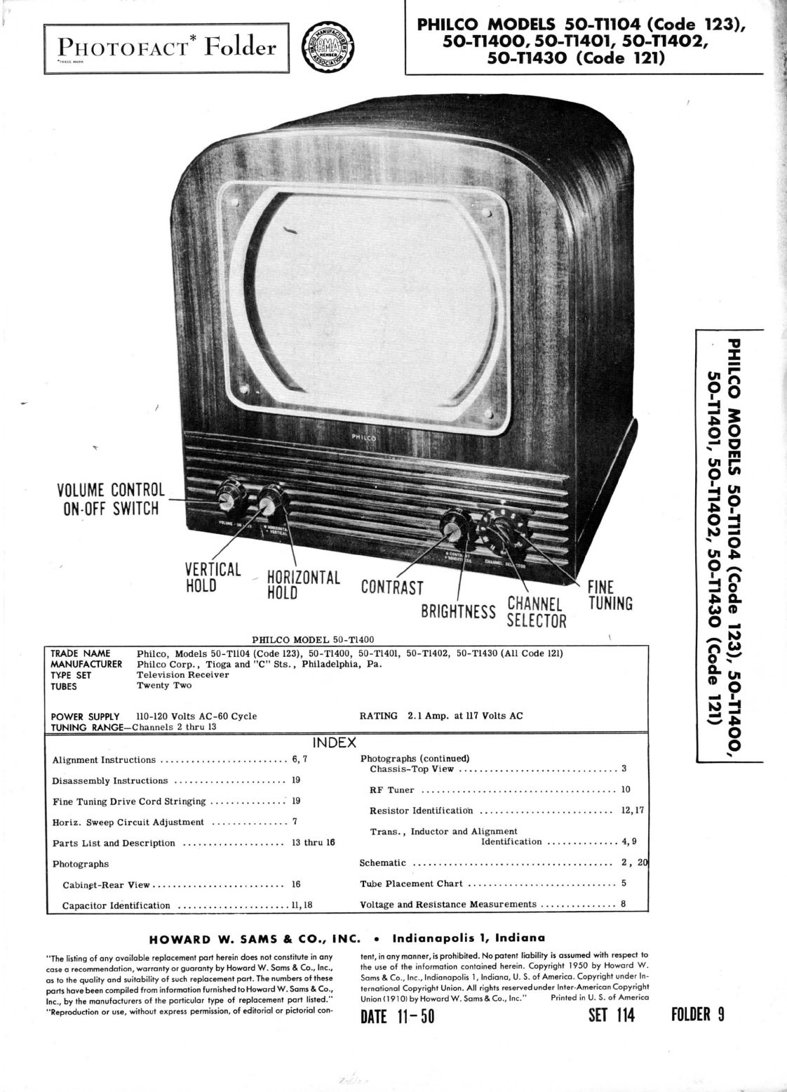
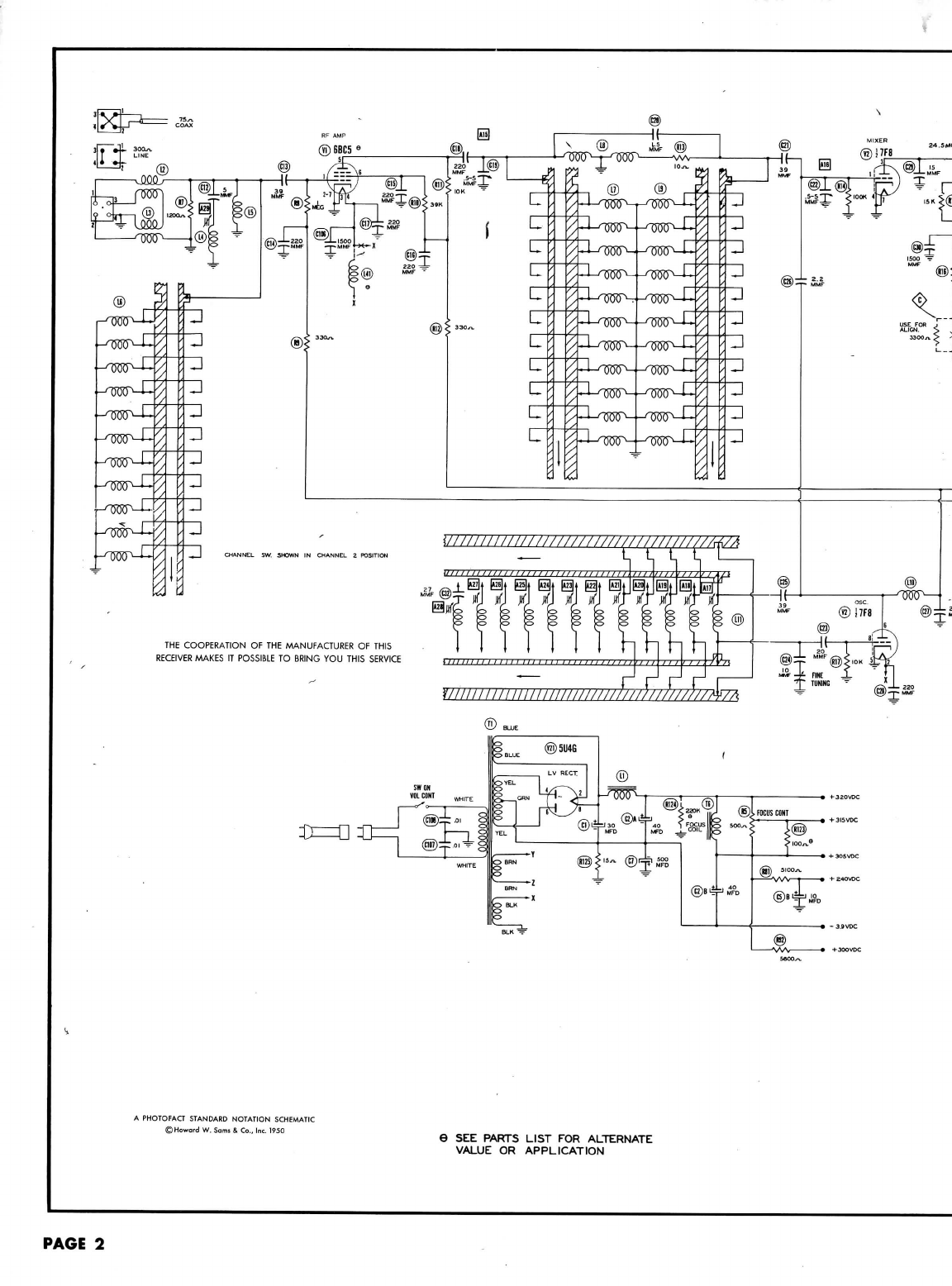
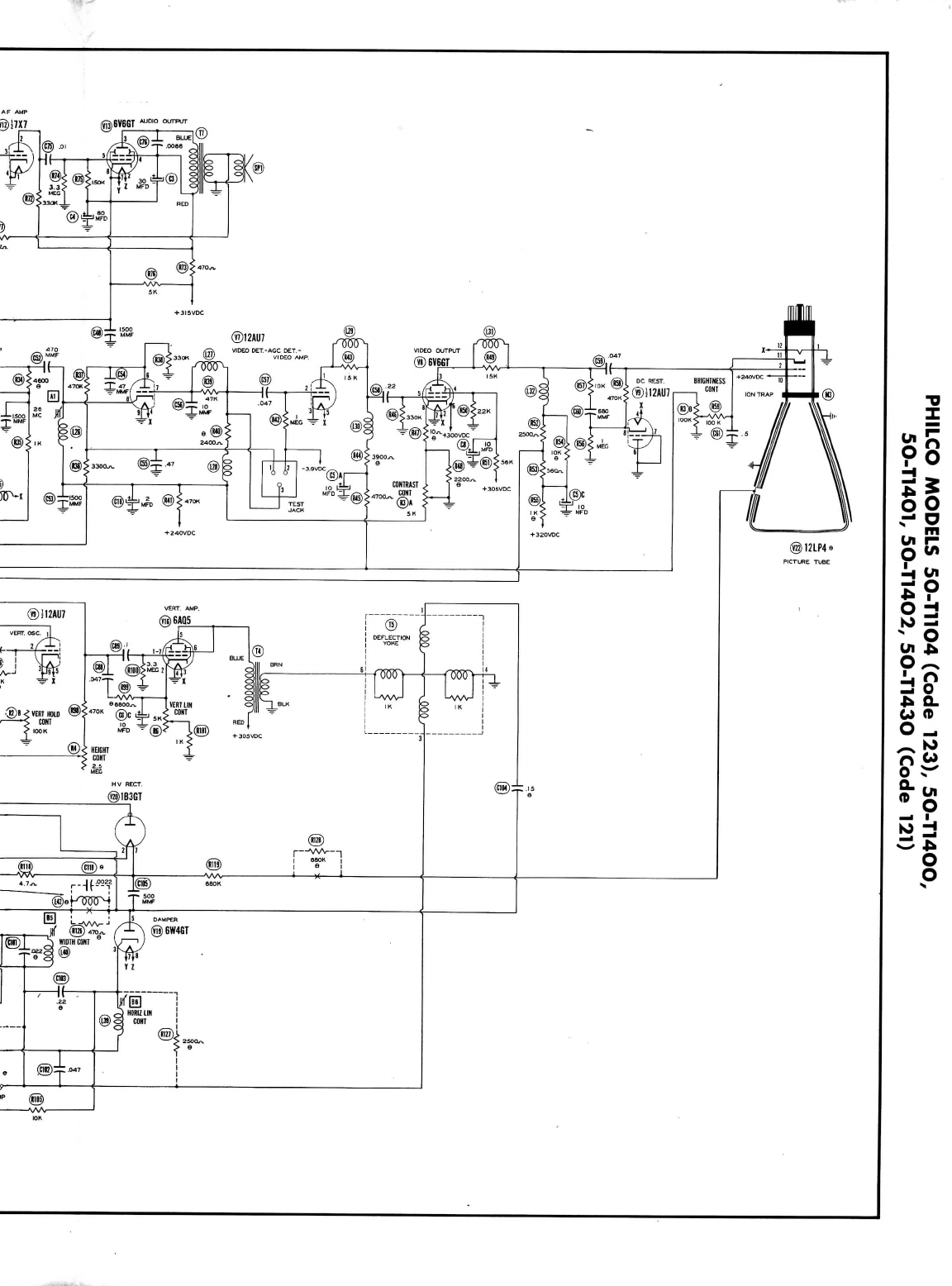
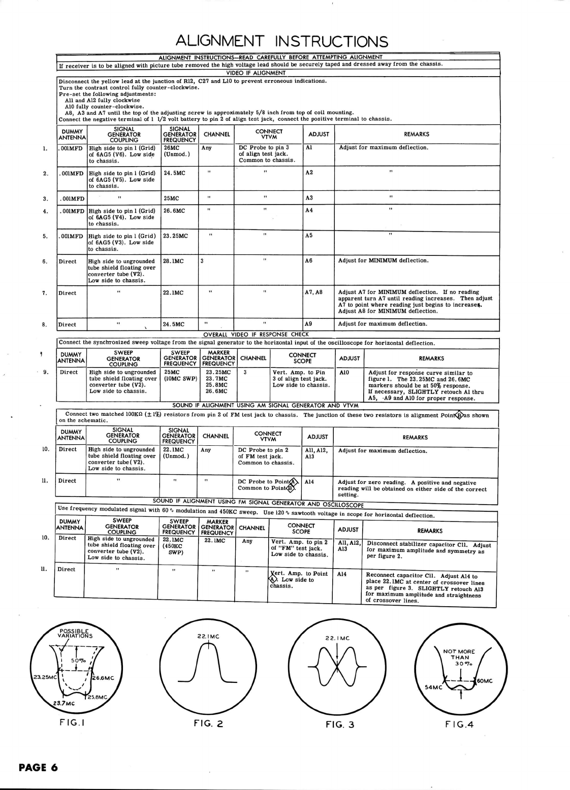
ALIGNMENT
INSTRUCTIONS
CCONTJ
RF
ALIGNMENT
Insert
a
piece
of
solder
into
hole
adjacent
to
tuning
core
A9.
Allow
the
solder
to
makecontact
with
thelug
under
the
hole
and
chassis.
Connect
a
3300n
resistor
in
series
with
150
volt
BH-
lead
to
R16.
The
junction
of
these
resistors
will
be
alignment
PoinK^.
The
sweep"
generator
output
leadshould
be
terminated
with
its
characteristic
impedance,usually
50
ohms.
DUMMY
ANTENNA
Two
120SJ
carbon
res.
SWEEP
GENERATOR
COUPLING
Across
antennatermin-
als
with
120S2
in
each
lead.
"
SWEEP
GENERATOR
FREQUENCY
57MC
(10MC
SWP)
213MC
(10MC
SWP)
MARKER
GENERATOR
FREQUENCY
54MC
60MC
Not
used
CHANNEL
2
13
CONNECT
SCOPE
Vert.
Amp.
to
Point
^^.
Low
side
to
chassis.
ADJUST
REMARKS
A15
Adjust
for
properbandwidth
of
6MC
to
14MC
as
shown
in
figure
4
with
markers
as
shown.
The
markers
should
notbe
less
than
70%of
maximumamplitude
of
response
curve.
A16
Adjust
for
maximum
amplitude
and
symmetry
asper
figure
4.
OSCILLATOR
ALIGNMENT
Reconnect
the
yellowlead
tothe
junction
of
R12,
C27and
L10.
The
signal
generator
output
lead
should
be
terminated
with
its
characteristic
impedance,usually
50
ohms.
Setthe
fine
tuning
control
tothe
mid-position
ofits
range.
DUMMY
ANTENNA
Two
120n
carbon
res.
SIGNAL
GENERATOR
COUPLING
Across
antenna
termin-
als
with
120S2
in
each
lead.
SIGNAL
GENERATOR
FREQUENCY
59.
75MC
(Unmod.)
65.75MC
71.75MC
81.75MC
87.75MC
179.
75MC
185.
75MC
191.
7
SMC
197.75MC
203.75MC
209.
75MC
215.75MC
CHANNEL
2
3
4
5
6
7
8
9
10
11
12
13
CONNECT
VTVM
DC
Probe
to
PoinK/p>.
Common
to
Point<K>.
ADJUST
A17
A18
A19
A20
A21
A22
A23
A24
A25
A26
A27
A28
REMARKS
Adjust
for
zero
reading.
A
positive
and
negative
reading
will
be
obtained
on
eitherside
ofthe
correct
setting.
FM
TRAP
ADJUSTMENT
TheFM
trap
is
adjusted
atthe
factory
to
100MC
and
normally
should
notbe
adjusted
unless
anFM
station
with
a
frequencyother
than
100MC
causes
interference.
Tune
intheTV
station
which
theFM
interferenceoccurs
and
adjust
A29for
minimum
interference.
If
theFM
station
notonthe
air,connect
anAM
signal
generator
tothe
antenna
terminals
asin
oscillator
alignment,
andset
generator
to
frequency
of
FM
stationcausinginterference,
and
turn
the
channel
selector
tothe
channel
on
which
interference
occurs.
Connect
the
vertical
input
lead
ofan
oscilloscope
to
alignmentPoint
C and
chassis.
Adjust
A29for
minimum
indication
on
scope.
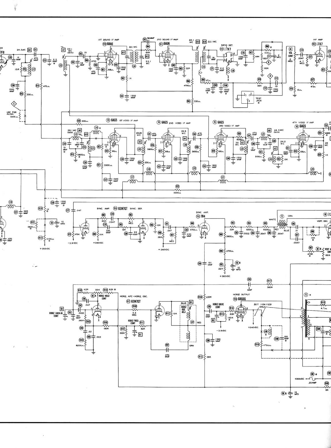
HORIZONTAL
SWEEP
CIRCUIT
ADJUSTMENTS
The
horizontal
hold
control
has
sufficient
range
to
compensate
for
normalvariations
and
still
provide
horizontal
synchronization.
If
replacement
of
tubes,
or
components,makes
it
necessary
to
make
further
adjustment,
they
should
be
made
as
follows:
1.
Turn
the
horizontal
frequency
trimmer
(Bl)
1 1/2
turnscounter-clockwise
from
fully
clockwiseposition.Turn
the
horizontaldrive
trimmer
(B2)
two
turnscounter-clockwise
from
fully
clockwiseposition.Turn
the
horizontallock-intrimmer(B3)
1/2
turncounter-clockwise
from
fully
clockwiseposition.Turn
the
horizontal
hold
control
tothe
midposition
ofits
range.
2.
Turn
thesetonand
tune
ina TV
station,
preferably
a
test
pattern,
and
adjust
the
horizontal
oscillator
coilslug(B4)
until
picture
synchronizeshorizontally.
3.
Turn
the
horizontal
hold
control
fully
clockwise,
and
adjust
B4
until
8 to10
horizontal
blanking
bars
are
visible
sloping
downward
to
the
right.
If
this
cannot
be
accomplished,
turn
Bl
anotherturncounter-clockwise
and
repeatthis
step.
4.
Turn
the
hold
controlcounter-clockwise
until
picture
isin
sync,
and
continue
rotation
of
hold
control
until
picturefalls
outof
sync.
The
picture
maynotgooutof
sync,
with
the
hold
control
atits
fully
counter-clockwiseposition.
If
this
is
true,
momentarilyremove
the
signal
by
switching
to
another
channel
and
backagain.
The
picture
should
beoutof
sync.Turn
the
holdcontrolslowlyclockwise
and
note
the
number
of
blanking
bars
presentjustbefore
picture
pulls
into
sync.There
should
be3 1/2to4 1/2
bars
present
justbeforepull-in.
If
there
are
more
than
4 1/2
bars,
turn
B31/4
turnclockwise
and
repeat
steps
3 and4.If
there
is
less
than
3 1/2
bars
present,turn
B3
another
1/4
turncounter-clockwise
and
repeat
steps
3 and4
until
this
condition
exists.
X
o
o
-g
•H
Ul
SP
o
ij
K>
—
-
o
01
J>
O
~_
JL
n
±
o
*
a.
CO
9
o
_
/-^
>»»
ft "
0
«.
o
o
HORIZONTAL
WIDTH
AND
LINEARITY
ADJUSTMENTS
Adjust
the
width
slug(B5)
until
picturefills
the
maskhorizontally.
Adjust
the
horizontallinearityslug(B6)untilpicture
is
symmetricalfrom
left
to
right.
PAGE
7