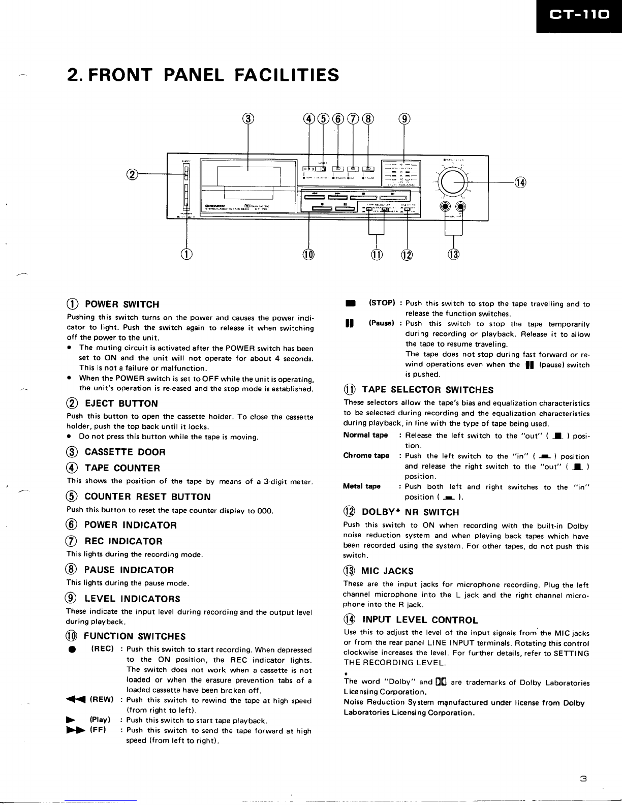
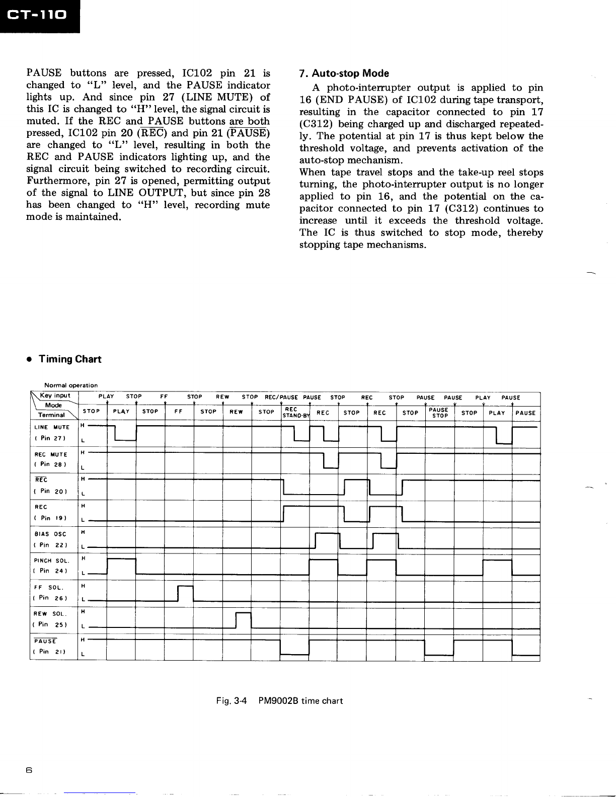
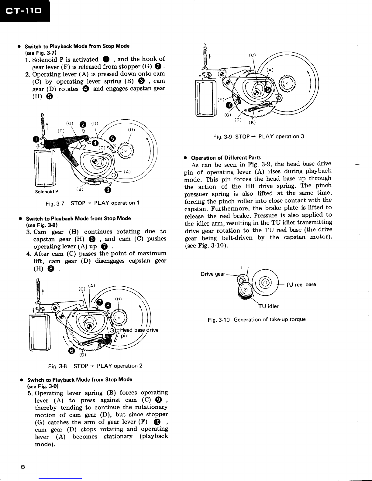
3.
CIRCUIT
DESCRIPTIONS
3.1 PLAYBACK
CIRCUIT
The signal from the playback head is amplified
by the Q102/Q103 2-stagedirect-coupled ampli-
fier. In the NORM position, the playback equali-
zation (120ps) compensation is achieved by the
NF circuit between the Q103 collector and Q102
emitter. In the METAL and CrOz positions,Q104
is turned on, and the equalization characteristics
switched from 120ps to 70ps to compensatethe
frequency response. The level of the EQ AMP
output is set by a variable resistor, and further
amplified by the Q401 flat amplifier before being
parised
through the MPX filter and applied to pin
2 of the Dolby IC.
This Dolby circuit consistsof IC401 (HA11226),
and the Dolby ON/OFF switch is linked to the
MPX filter ON/OFF switch. When the Dolby
switch is OFF, the 19kHz filter is bypassed.
The Dolby circuit output appears at pin 8 of
IC401, and is passed to LINE OUTPUT via a
switchingIC (IC402).
3.2 RECORDINGCIRCUIT
The input signal from the microphone jack is
amplified by the microphone amplifier IC101, and
passed via the MIC/LINE selector switch to the
INPUT volume control where the input level is
adjusted. This adjusted signal is passedvia IC103
to flat amplifierQ40l. D313 andD314 in the stage
before IC103 form a protector circuit designed
to protect IC103 from large input signals. The
signal amplified by the flat amplifier is pa.ssed
via
the MPX filter to pin 2 of the Dolby IC, the output
appearing at pin 8. The level of this output is
adjusted by variable resistor. Then after equaliza-
tion in the REC AMP (Q106) in accordance
to
the type of tape being used, the signal is passed
to the recordinghead. +g
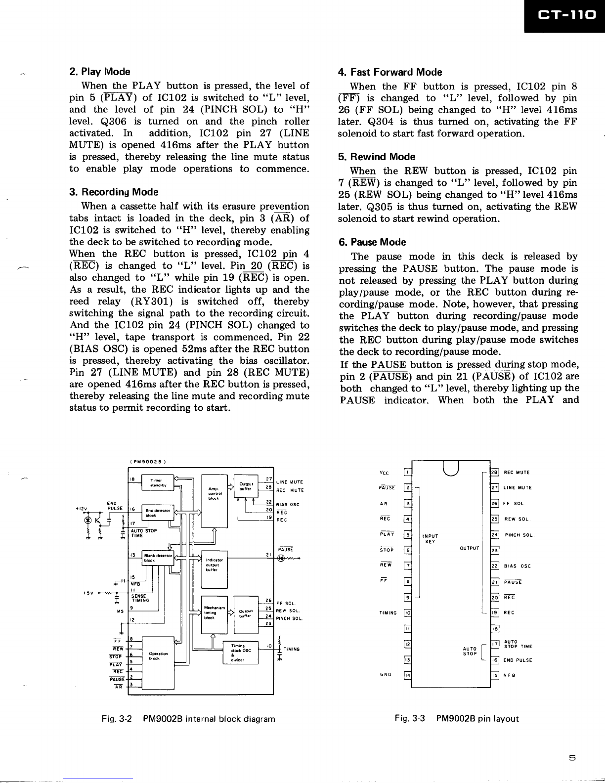
3.3 CONTROLCIRCUIT
The control circuit in this deck utilizes a one-
chip IC (PM90028) which enablesfeather-touch
operations. In addition to mechanism control,
this IC also includes auto-stop function. And due
to the digital counter frequency divider system
employed in timing settings for the mechanism
control, all operational timing discrepancies have
been eliminated. The PM9002B pin layout is
shown in Fig. 3-3, the functional block diagram
in
Fig. 3-2, and the output pin time charts during
different modes in Figs. 3-4 and 3-5. For inter-
relations between circuits, see the block diagram
onpage
10,11 andin Fig.3-1.
4
Operations
duringEachMode
The mechanical operations effected by the
following circuit changes
are described in the next
chapter (seepage
7).
1.When
the POWER
Switch is
SwitchedON
When the POWER switch is switchedon, *5V is
applied to pin 1 (Vcc) of IC102. During the initial
period when pin 1 voltage is being increased from
0V to 5V (approximately from 0.6V to 2.4V) the
IC's intemal reset circuit is activated, putting the
IC into stop status which is maintained for about
four seconds
after the power switchisswitchedON.
During this time, no change can be effected by
pressing
any of the other operation control buttons.
REC/PB
head
LINE
OUTPUI
rcroz
PM9OO2
B
pquse
an
REC REC
pr-a
y REc
STOP PAUSE
REW BIAS
osc
oFa
MUTE
SIGNAL
MS
LINE
PINCH MUTE
REw "iI&,
Er ENO
OETECT
TIME
Fig.3-1 Controlsystem
blockdiagram