TECHNICAL DESCRIPTION
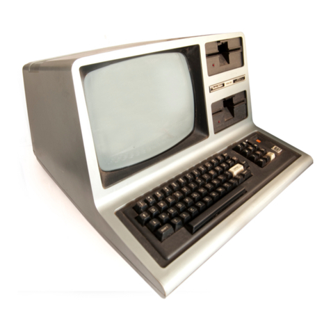
The technical description of the Model III Computer CPU
circuit board will be broken down into nine sections. These
are;
1. Processor
2. RAM
3. Adress Decoding
4. Video
5. Video Sync Circuits
6. Keyboard
7. Cassette Interfaces
8. Line Printer and Real Time Clock
9. I/O Bus
This breakdown, which follows the partitioning of the sche-
matic diagrams, will allow easy explanation and referencing.
VIDEO SYNC CIRCUITS
The video sync circuits are required to meet the pulse width
and polarity requirements of the video monitor. It also allows
adjustment in both the horizontal and vertical planes in dis-
crete increments. The vertical sync pulse VSYNC is active
low and approximately 693/«ec in duration. The frame rate
is either 50 or 60 Hertz, The horizontal rate is 15,840 Hz and
the signal HSYNC is active high with aduration of approxi-
mately 8,usec. Tne vertical plane adjustment covers a total
of eight rows and is adjustable in increments of one row
(R1, R2, R4). The horizontal plane adjustment increments
by two characters for a total coverage of 16 character posi-
tions. Both adjustments are accomplished with the use of
wired "AND" gates U22 and U38 {LS266J.
PROCESSOR
The CPU chip is aZ80 that runs at aclock speed of 2.02752
MHz:. The CPU clock is derived by dividing the basic video
clock (10.1376 MHz) by five. U62 performs this function
and the clock is non-symmetrical with a40 percent high duty
cycle. The clock signal PQC is run through an active pull-up
and becomes PCLOCK which has afull B-volt swing with fast
rise and fall times. The reset switch, which is located on the
keyboard, is ORed with power on reset (R7, C54, U15) to
provide aSystem RESET* signal. The Reset pin on the Z-80
is driven by RESET*. The address lines are buffered by
LS244*s {U91, U92), the data lines by an LS245 (U90),and
control lines buffered by an LS367 (U76), The buffered
control lines are combined in U89 and U86to form memory
and IO port controls (RD*, WR*, IN*, OUT*).
See the CPU Timing Diagram for exact time relationships.
U75 is used to switch the data bus buffer during (NTAK*
cycle or any read operation (IO or Memory), Whenever one
of the ROM's is being accessed, the data bus buffer is dis-
abled by U108 since the ROM's data lines are located on the
CPU data bus. BUSRQ*, HALT*, BUSAK*, and RFSH*are
not used. The Model III has three sockets for the ROMs
U104, U105, U106). They are 64K bit,32K bit and 16Kbit
ROMs, respectively.
RAM
The RAM consists of an array of up to twenty-Four 16K
dynamic memory chips with damping resistors located on all
address and control lines (RP1 ,RP2, RP3), Chips U7 to U14
are addressed at 4000 to 7FFF, U25 to U32 are addressed at
8000 to BFFF and U43 to U50 are addressed at C00O to
FFFF. The memory data is interfaced to the data bus by
two 8T26; (U63, U64), Normally the data is driven into the
memory array. However, on aread cycle U19 switches the
direction of the transceivers and drives memory data onto
the data bus. The 5volts required by the RAMs is supplied
by a3-terminal regulator (MC7905C) which takes -12 volts
as its input. See the CPU Timing Diagram for the relationship
between RAS*, MUX, CAS*.
9B 6<!nw« >\— -Of Ct>t)E P"E TCH CYCLE -Htfl,rj c*ClE -
gi!)7&w4; CLOCK Triri^jijijmixnjTjinjij^^ nnjTjmanRjxruu\riJirui^^ CMiWGES DgFELOCfc
t.11 Lirwj EBtt D* GlCG *
FIGURE!. CPU TIMING DIAGRAM
13