manuals.online logo
Brands
  1. Home
  2. •
  3. Brands
  4. •
  5. Radio Shack
  6. •
  7. Desktop
  8. •
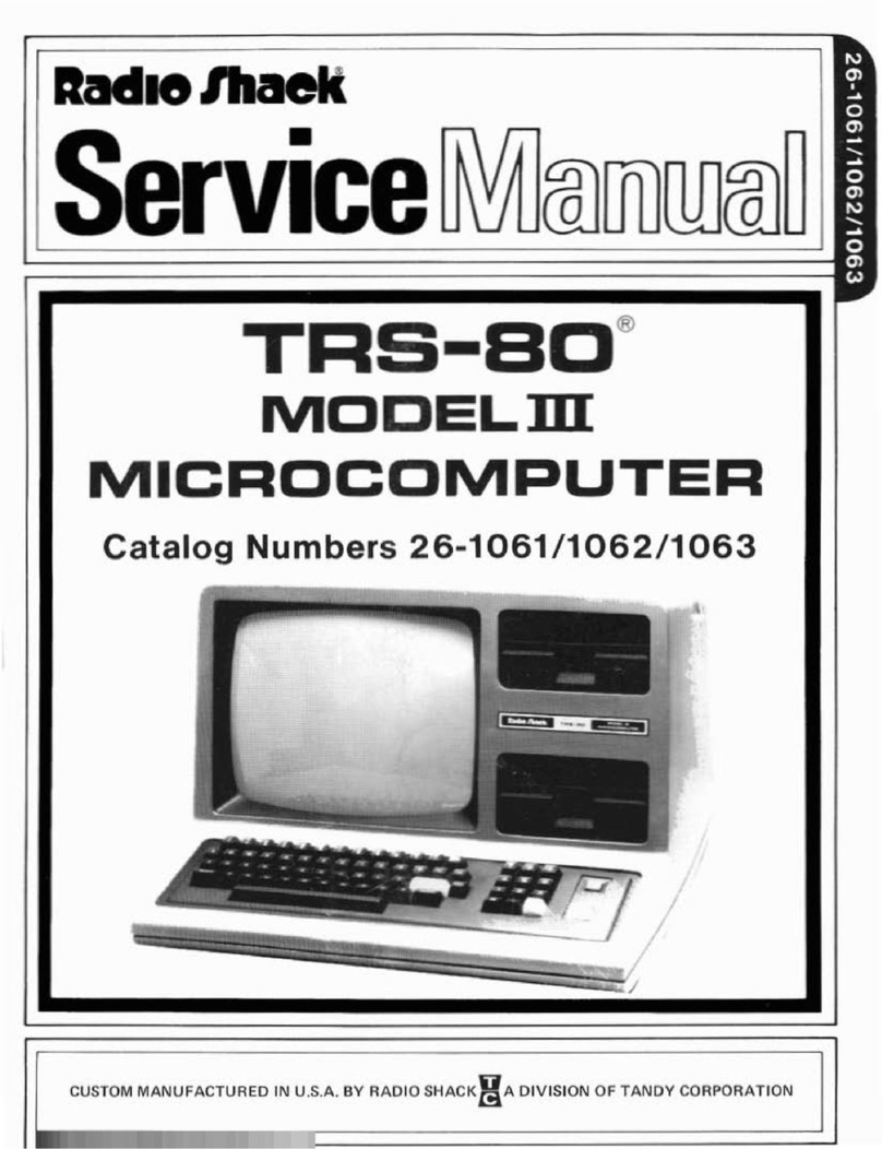
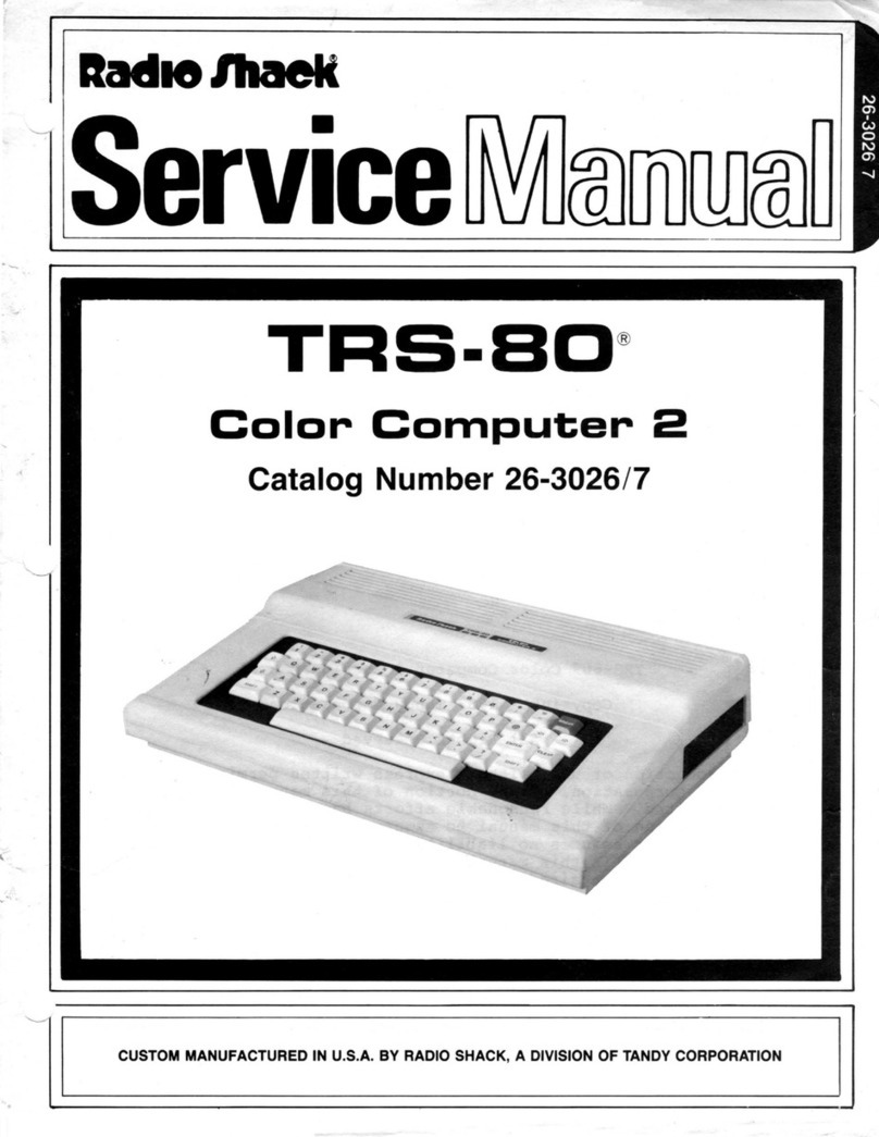
  9. Radio Shack TRS-80 User manual

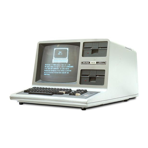
Radio Shack TRS-80 User manual

s.-s
__
C_O_M_PU_"TJ_E_R~_A_C_T._s_n.
R_AM_DO_I~_;_~A_1
~_:v_~_~S_I~8_0
KEYBOARD,
CPU
BOARD
o
co
r},=
a:...J
t-
W
~>
o~
ct-
J:...J
C/)w
0°
-0
0:e
ct
a:
C")
en
o
en
oMODEL ILEVEL
1\
EXPANSION INTERFACE
See
Folder
CSCS3-A
SAFETY PRECAUTIONS
See page 19
MONITOR
See
Folder
CSCS3-B
PRELIMINARY SERVICE CHECKS
ENCLOSED
INDEX
Page
Block
Diagram
29
Disassembly
Instructions
4
General
Operating
Instructions
4
GridTrace
Location
Guide
CPU Board
13
IC
Pinouts
&Terminal
Guides
6,27
Line
Definitions
19
Logic
Charts.
. .
..
..24,25,26
Miscellaneous
Adjustments
20
Parts
List
15,16,17,18
Page
Photos
Cassette
Modification
Counter
Board 20
CPU Board 10,11,12,21,22,23
Level
II
ROM Board
14
Partial Keyboard 14
Safety
Precautions
19
Schematics
CPU 2,3,30,31,32,33
Power
Supply
5,28
Schematic
Notes
9
Troubleshooting
7,8,9
IS,.
Howard
W.
Sams
&Co
..
Inc.
4300
West
62nd
Street,
P.O.
Box 7092,
Indianapolis,
Indiana
46206
U.S.A.
The llliing of ony
available
replocement
port
herein
dolu
not
constitute
In
any
co,.
a
recommendation.
warranty
or
guoranty
by
Howard
W.
Sam,
&Co. Inc
.•
as
to
'hoe
qualIty
and
SUltoblhty
of such
replacement
port. The
numbers
of
'hes.
parts
have
been compiled
from
information
fU"~lIhed
to
Howard
W
$oms
&Co.. Inc
by
the
manufacturers
of
the
particular
type
01
replacement
port
listed
Reproduction
or
use
without
expre
..
permission,
of
editorial
0(
piC1oriol
content
in
any
monner.
is
prohibited.
No
poten'
Iiobility
i,
os.Jumed
with
respect
to
the
VI.
of the
information
contained
herein.
e1985
How""
W.
sam,
&Co., Inc.
"300 West 62nd Str
..
t,
P.O.
lox
7092. Indianapolis. Indiana
<16206
U.S.A.
Pdn'ed
in U.S. of
Amefico.
85CC14942 DATE 2.85
~
.....
~
COMPUTCR'C"CTS"'
RADIO SHACK
TRS·SO
~.
'_
lC_III_/""\
__
'_
' M
....
O
..
D
..
E_L_I_L
..
EV_E_L
..
I
..
I_
PRELIMINARY SERVICE CHECKS
This data provides the user
with
atime-saving service
tool
designed for
quick
isolation
and repair of
computer
system
malfunctions.
Check all
interconnecting
cables
for
good
connections
and
correct
hookup
before making service checks.
MISCELLANEOUS ADJUSTMENTS
Disconnect all external peripherals from
the
computer
system
to
eliminate possible external
malfunctions.
Replacement
or
repair
of
Power Supplies,
CPU
(Main)
Board, Expansion Interface Board and
Monitor
Boards or
connectors
may be necessary
after
the
malfunction
has
been isolated.
RAM SELECT SHUNT
(Z71)
CPU
AND KEYBOARD
Type and run the
following
Basic program
to
produce arec-
tangle on the
Monitor
screen:
HORIZONTAL AND VERTICAL CENTERING
CPU
AND
KEYBOARD
RAM Select Shunt
(Z71)
is set up in accordance
to
the
amount of RAM memory (4K or 16K) installed on
CPU
Board.
Use
the
following
chart
to
determine which pins are
shunted.
10
CLS: FOR X=0TO
127
20
IF X>47 THEN
40
30
SET
(O,X):
SET (127,X)
40 SET
(X,O):
SET (X,47)
50 NEXT X
60 GOTO 60
ROM
SELECT SHUNT
(Z3)
CPU
AND KEYBOARD
NOTE: Perform
12V
adjustment
before
5V
adjustment.
Z3
LEVELl
LEVEL
II
PINS BASIC BASIC
271
4K 16K
PINS RAM RAM
1-16
Open Shunted
2-15
Shunted Shunted
1-16
Open Shunted
3-14
Open Shunted 2-15 Shunted Open
4-13
Shunted Shunted 3-14 Open Shunted
5-12
Open Shunted 4-13 Shunted Open
6-11
Shunted Shunted 5-12 Open Shunted
7-10
Shunted Shunted
6-11
Shunted Open
8-9
Open Shunted 7-10 Open Open
8-9 Open Open
12V AND
5V
ADJUSTMENT
CPU
AND KEYBOARD
Connect the
input
of
a
DC
voltmeter
to
pin 3of Regulator IC
(Z2).
Adjust
the 12.0V
Adjust
Control (Rl0)
for
11.9V.
Connect the
input
of a
DC
voltmeter
to
pin 3of Regulator IC
(Z1).
Adjust
the
5V
Adjust
Control
(R5)
for
5.0V.
12V AND
5V
ADJUSTMENT EXPANSION INTERFACE
Rom Select Shunt
(Z3)
is set up in accordance
to
whether
MLevel I
or
Level
II
Basic ROMs are installed. Use the follow-
.
CJ)
ing chart
to
determine which pins are shunted.
()
CJ)
()
o
co
ch=
a:...J
....
w
::.::>
()~
«-
~...J
CJ)w
00
-0
o~
«
a:
NOTE: Perform 12V
adjustment
before
5V
adjustment.
Connect
the
input
of
a
DC
voltmeter
to
pin 3
of
Regulator IC
(Z20).
Adjust
the
12V
Adjust
Control
(R7)
for
11.9V.
Adjust
the Horizontal Center Control (R20) and Vertical
Center Control
(R21)
to
center the rectangle on the
Monitor
screen.
Connect
the
input
of
a
DC
voltmeter
to
pin 3
of
Regulator IC
(Z21).
Adjust
the
5V
Adjust
Control
(R8)
for 5.0V.
s
I~
Howard
W.
Sams &Co., Inc.
lelrTII
4300
West
62nd Street, P.O. Box 7092,
Indianapolis,
Indiana
46206 U.S.A.
DATE
2-85
85CC14942
R_oductlon
0.-
.....
without
_p'."
pennl
..
lon.
01
edltoriol
0.-
picto.-lol
conl..,t,
In
ony
manner.
i.
prohibited. No pot..... liobUlty
I.
auumed
with
r.sp«'
to
the u
..
of the Infarmotlon contolned
"-<eln.
~
11185
Howanl
W.
Sam.
&Co.,
Inc:.
4300 W
..
,62nd
St,
..
t. P.O.
lax
7092. Indianapolis. Indiana
~
U.S.A.
Printed
In
U.S.
of
"memo.
Th.
lI,ting of
any
ovailable
r.plocement
port tMreln
does
not
constitute
in
any
cos.
0rec:ommeondotion.
warranty
or
guaranty
by
Howard W.
Saml
&Co
.•
Inc
..
as
to
the
quality
and
suitability
of such
r.ploc.ment
port. The
numbers
of
the,.
pam
hove
been compiled
from information furnished to Howard
W.
$oms &Co..
Inc
.. by the
manufacturers
of
the
particular
type
of
replocement
port
listed.
PRELIMINARY SERVICE CHECKS (Continued)
SERVICE CHECKS
SEE INTERCONNECTING DIAGRAM AND PHOTOS
TO
MATCH THE NUMBER
IN
THE
CIRCLES WITH THOSE
IN
THE FOLLOWING DATA FOR SERVICE CHECKS TO
BE
PER-
FORMED.
CD
POWER SUPPLY
(CPU
BOARD)
(A)
Disconnect the
CPU
Power Supply Module (PT1)
from
Connector
J1A and check
for
18.5VAC be-
tween pin 1and pin 3and 23.6V between pin 2
and pin 4
of
the Power Supply Plug (P1A). If
the
voltages are missing, replace the Power Supply
Module.
(B)
Check
for
5.0V at pin 3
of
Regulator IC
(Z1).
If
the
measurement is
not
correct, check the adjust-
ment
of
the
5V
Adjust
Control
(R5).
(C) Check
for
11.9V at pin 3of Regulator IC
(Z2).
If
the
measurement is
not
correct, check the ad-
justment
of
the 12V
Adjust
Control (R10).
COMPUTER DOES NOT COME
UP
PROPERLY
(A)
See
if
the
ROM
Select
Shunts
(Z3)
and RAM
Select
Shunts
(Z71)
have been set up properly,
see "ROM Select Shunt Z3"
section
of
Miscel-
laneous Adjustments.
(B)
Check Regulator IC
(Z1)
and
Microprocessor
IC
(Z40)
by
substitution.
(C) Check RAM ICs Z13 thru Z20 by
substitution.
KEYBOARD
(A)
If only one key is
not
working properly, clean the
key
contacts
with
aspray
contact
cleaner. If the
key is
still
defective, check
for
breaks at
the
key
contacts
and solder
joints.
Check the key con-
tacts
with
an ohm meter.
(B)
If several keys are not working, check the ribbon
cable between Keyboard and
CPU
board
for
possible
open
circuits.
(C)
If
wrong character appears on the
Monitor
screen when akey is pressed. Check Character
Generator IC
(Z29)
by
substitution.
@NO VIDEO ON MONITOR
(A)
Check the video cable
for
broken wires and the
Video
Connector
(J2)
for
good
connection.
(B)
Check the
adjustment
of
the
Contrast
Control
(R102) and Brightness Control (R103) located on
the
Monitor.
VIDEO DISPLAY NOT CENTERED
ON
MONITOR
(A)
Check the
adjustment
of
the Horizontal Center
Control
(R20)
and Vertical Center Control
(R21)
on
the
CPU
Board,
see"
Horizontal and Vertical
Centering"
section
of
Miscellaneous
Ad-
justments.
II
CD
VIDEO DISPLAY UNSTABLE
(A)
Check the
adjustment
of
the Horizontal Hold
Coil (L4) and Vertical Hold Control (R13B)
located on the rear of the Monitor.
®MONITOR DEAD
(A)
Check Fuses
F101
and F103 located inside the
Monitor.
®CASSETTE PORT INOPERATIVE
(A)
Check the Cassette cables for loose
or
broken
wires and also check
Connector
J3 on
CPU
Board and
Connectors
J6, J7 and J8 on Expan-
sion Interface Board
for
good connections.
(B)
If the Cassette
motor
will not
stop
running, turn
the Computer Off. Use
an
ohm
meter
to
check
for
an open
circuit
from the center pin at one end
of
Relay
K1
to
the center pin at the
other
end
of
Relay
K1.
If the pins are shorted,
either
Relay
K1
contacts
are
sticking
or Diodes CR9 and CR10
are shorted.
POWER SUPPLY (EXPANSION INTERFACE)
(A)
Disconnect the Expansion Interface Power Sup-
Iy Module (PT1) from
Connector
J9 and check
for
19.7VAC between pin 1and pin 3and 23.6V
DC
between pin 2and pin 4
of
the Power Supply
Plug
(P9).
If the voltages are
missing,
replace the
Power Supply Module.
(B)
Check
for
11.9V at pin 3
of
Regulator IC
(Z20).
If
the measurement is incorrect, check the adjust-
ment
of
the 12V
Adjust
Control
(R7).
(C) Check
for
5.0V at pin 3
of
Regulator IC
(Z21).
If
the measurement is incorrect, check the adjust-
ment
of
the
5V
Adjust
Control
(R8).
DISK DRIVE PORT INOPERATIVE (EXPANSION
INTERFACE)
(A)
Check Disk Drive cables
for
loose or broken
wires and
Connector
J5
for
good
connections.
Clean Connector J5
contacts
with
a
contact
cleaner.
(B)
Check Disk
Controller
IC
(Z42)
by
substitution.
LINE PRINTER PORT INOPERATIVE (EXPANSION
INTERFACE)
(A)
Check the Line Printer cable for loose or broken
wires and Connector J4
for
good connections.
Clean
Connector
J4
contacts
with
a
contact
cleaner.
J3
SU'"FERED
INTERFACE
IllS
PORT
40
52
RESET
39
HI~
@)
Z40
2
40
'--------I
"Y"
®
FWl
lCa
40
CASSETTE
CASSETTE
2I
L
.J
Y
@)
J1
34
JS
2
DISK
MIVE
PORT
Q34
DISK
~
CCWTROlLER
8L
t:.:
PRINTER
PORT
Q2
142
\!.J
8RIO
@
CJ@
Rf6lLAT~
Rf6tl.AT~
5.~
m
@)
EJ
/6
11.9V
BBBBBBBB
EXPANSION
INTERFACE
BOARD
PRELIMINARY SERVICE CHECKS (Continued)
CPU
BOARD
19.7VAC
MON
ITOR
V
IDEO
BOARD
CASSETTE
HOOIF
lCATlOH
COUOfTER
!IOARD
{
HOR~
@
CENTER
R21
VERT
r-----~
CENTER
0-----
VERT
Q
SIZE
rnD
_
LEVEL
IT
ROM
BOARD
MONITOR
MAIN
BOARD
P I
CPU
POWER
SlI'flt
y
@
HORI1
@
VERT
I«llD
HCl.D
PRELIMINARY SERVICE CHECKS (Continued)
@
F103
0
]A
®
F~'
0
I20VAC
8
~-~
....
'V'----.,
MONITOR
CHASSIS
Z33
FWl
SHMTS
KEYBOARD
INTERCONNECTING DIAGRAM
X
INTERCONNECTING DIAGRAM
III
PRELIMINARY SERVICE CHECKS (Continued)
GENERAL OPERATING INSTRUCTIONS
POWER
UP
(COMPUTER ONLY)
Turn On the Computer. The
words
nMEM SIZE?"
will
ap·
pear on the
Monitor
screen. Press the Enter key once. The
word"
READY" and a
prompt
character
will
appear on the
Monitor
screen. The
Computer
is
now
in Basic mode.
POWER
UP
SEQUENCE (WHEN USING DISK DRIVE)
1.
Turn On the Expansion·Interface.
2.
Turn
On
the Disk Drives (Terminal Drive 26·1164A, first)
and then any
other
peripherals.
3.
Put a
diskette
(containing
DOS, Disk
Operating
System)
into
Disk Drive
O.
Turn On the Computer. The
Computer
will
automatically
boot
up from Disk Drive
O.
The version
of
the
Disk
Operating System
will
appear on the
Monitor
screen along
with
the words "DOS READY" and a
prompt
character.
NOTE:
If
an Expansion
Interface
unit
is used
without
a
Disk Drive,
hold
down
Break key when
turning
On Com·
puter. A
double"
MEM SIZE?"
will
appear on
Monitor
screen. Press Enter key and the
word"
READY"
will
ap·
pear followed by a
prompt
character. The
Computer
is
now in Basic mode.
RESET
Press the Break key and the Reset
button
(on
right
rear
of
the Computer) to reset the
Computer
to
Basic mode.
If
Disk
Drives are attached,
insert
a
diskette
containing
DOS infor-
mation
into
Disk Drive 0and press
only
the Reset
button.
This
will
reboot
the
Computer
from Disk Drive
O.
DISK OPERATING SYSTEM (DOS)
Type DIR and press the Enter key
to
display
a
directory
of
programs
that
are on the
diskette
in Disk Drive
O.
Type DIR :
and the
number
of
the Disk Drive
holding
the
diskette
which
contains
the
information
desired. Example: Type DIR
:2
to
list
programs
on
diskette
in Disk Drive
2.
To load aprogram from a
diskette,
type the name of the pro-
gram and press the Enter key. Use a
colon
and the
number
of the Disk Drive
which
contains
the program
to
be loaded_
If no
number
is given, the
system
will
assume
Disk Drive
O.
NOTE:
Basic
program
will
not load from
diskette
unless
the
Computer
is
in the Disk Basic mode.
To get back to the DOS from Disk Basic mode, type
IV
CMD"S"
and press the Enter key. Any program in
memory
will
be
lost
when leaving Basic
mode
by
using
"CMD"S".
DISK BASIC
To load Disk Basic
into
the Computer,
boot
up on DOS. In-
sert a
diskette
containing
Disk Basic (usually apart
of
the
DOS
diskette)
into
Disk Drive
0,
type BASIC, press the Enter
key and
follow
prompts.
To
go
from Disk Basic
mode
to
DOS, type
CMD"S"
and press the Enter key. Any program
in memory
will
be lost.
To load aprogram from a
diskette,
type LOAD and the pro-
gram name enclosed in
quotes
and press the Enter key. To
load from aDisk Drive
other
than Drive
0,
add a
colon
and
the
Disk
Drive
number
at the end
of
the program name. Ex-
ample: LOAD
"SAMS:1"
for Disk Drive
1.
To save aprogram
onto
a
diskette
in aDisk Drive, type
SAVE and the program name in
quotes
and press the
Enter
key. To save aprogram
onto
a
diskette
in aDisk Drive
other
than Disk Drive
0,
add a
colon
and the Disk Drive
number
at
the end
of
the program name. Example: SAVE
"SAMS:1"
for
Disk Drive
1.
FORMATIING
A
DISKETIE
NOTE: This procedure
does
not
copy Disk Operating
System
sections
required for normal
disk
operations. A
diskette
thus
formatted
must
be used
only
with
systems
containing
2
or
more Disk Drives.
Use"
Back-up"
function
to
format a
diskette
containing
DOS
information.
Ablank
diskette
must
be
formatted
before it can be used
for
saving data. To
format
a
diskette,
boot
up
on DOS, insert a
diskette
with
the
format
program on it (usually part
of
the
DOS
diskette)
into
the Disk Drive, type FORMAT and press
the Enter key.
After
the program has been loaded, insert a
blank
diskette
into
the Disk Drive and
follow
the instruc-
tions
on the
Monitor
screen.
CASSETIE
OPERATION
To load aprogram from tape, type CLOAD (with
or
without
the program name enclosed in quotes),
put
the Recorder in
play
mode
and press the Enter key. Prompt
will
indicate
when program has been loaded.
To save aprogram
onto
tape, save CSAVE (with
or
without
the program name enclosed in quotes),
put
the Recorder in
record mode and press the Enter key. A
prompt
will
in-
dicate
when
writing
has been completed.
PRELIMINARY SERVICE CHECKS (Continued) PRELIMINARY SERVICE CHECKS (Continued)
CE
TER
HORll
R20
{
CR9
@
K1
CR10
CPU BOARD
VIII
®
CASSErE
J3
@
Af1A\
f3C\
~
POWER
V
DEO
~
POWtR
SW
TCH
J2
Z29
J1
Sl
r®
..
@@®@
ROM
SELECT
SHU
TS
Z3
@
RAM
SELECT
SHU
TS
Z71
Z40
@
KEYBOARD
®
CABLE
CPU BOARD
V
PRELIMINARY SERVICE CHECKS (Continued)
12V
ADJ
{
R7--
@120V
PI
3
Z20
5V
AoJ
@{
R8
~
OV
PI
3
Z21-....JIi==
POWER
J9
@
..
PRELIMINARY SERVICE CHECKS (Continued)
G~0
OS
DR
E
paR
J5
LINE
PRI
TER
~~_j~RT
@
BUFFERED
INTERFACE
BUS
PORT
~~-J3
:tl
3:>
0
52
00
m(f)
r-z
->
r-(')
m~
<0004
~:tl
_(f)
-eo
o
EXPANSION INTERFACE BOARD
VI
EXPANSION INTERFACE BOARD
VII
PRELIMINARY SERVICE CHECKS (Continued) PRELIMINARY SERVICE CHECKS (Continued)
CE
TER
HORll
R20
{
CR9
@
K1
CR10
CPU BOARD
VIII
®
CASSErE
J3
@
Af1A\
f3C\
~
POWER
V
DEO
~
POWtR
SW
TCH
J2
Z29
J1
Sl
r®
..
@@®@
ROM
SELECT
SHU
TS
Z3
@
RAM
SELECT
SHU
TS
Z71
Z40
@
KEYBOARD
®
CABLE
CPU BOARD
V
PRELIMINARY SERVICE CHECKS (Continued)
PREVENTATIVE MAINTENANCE
ENVIRONMENT
Computers
perform best in aclean, cool area
that
is
below
80
degrees Fahrenheit and free
of
dust
and smoke particles. Even
though
home
Computers
are not affected by
cigarette
smoke as
much
as
commercial
Computers
are affected,
it
is
belter
to
maintain
asmoke-free area around the Computer. Do
not
block
cabinet vents
of
any
of
the
Computer
system; Computer,
Monitor,
Printer,
or
other
power
devices.
ELECTRICAL POWER
Variations in the line voltage can
affect
the Computer. Try
to
avoid these
fluctuations
by
using
an
AC receptacle that is on a
power
line
not
used by appliances
or
other
heavy
current
demand devices. Apower-surge protector, power-line
conditioner,
or
non-interruptable
power
supply
may be needed
to
cure the problem. Do
not
switch
power
On
and
Off
frequently.
KEYBOARD
liquids
spilled
into
the Keyboard can ruin it.
Immediately
after
a
spill
occurs,
disconnect
the
Computer
power plug from
AC
power
outlet.
Then,
if
circuitry
or
contacts
are
contaminated,
disassemble
the Keyboard and
carefully
rinse the Keyboard
printed
circuit
board
with
distilled
water and let it dry. Use a
colton
swab
to
clean between the keys. Use anon-abrasive con-
tact
cleaner and lint-free wipers on accessible
connectors
and
contacts.
DISK DRIVES
Clean the read/write heads
of
the Disk Drives about
once
a
month
or
after
100
hours
usage. Use
only
an approved head clean-
ing kit.
Handle
carefully
to
preserve proper
disk
head alignment. Asudden bump
or
jolt
to
the
Disk
Drives can
knock
the
disk
head
out
of
alignment.
If the
disk
drive
must
be transported, place an
old
disk
in
slot
and
close
door
during
transport.
Store
disks
in
their
protective
covers and never
touch
the
disk
surface. Observe the
disk
handling precautions
usually
found
on the back of
disk
protective
covers.
PRINTERS
Carefully vacuum the Printer regUlarly. Wipe surface areas clean using a
light
all-purpose cleaner. Do
not
oil the machine.
The oil
will
collect
abrasive
grit
and
dust.
The
dust
will
act
as ablanket.
This
can cause
components
to
overheat and fail.
STATIC ELECTRICITY
Static
electricity
discharge
can
affect
the Computer. In order
to
minimize
the
possibility,
use
anti-static
mats, sprays,
tools
and materials, and maintain good
humidity
in the
Computer
environment.
MONITOR
Use an
isolation
transformer
with
any
Monitor
that
does
not
come
as part
of
the system
since
some
Monitors
use aHOT
chassis
(chassis
connected
to
one side
of
the AC line). The face
of
the
Monitor
should
never be
left
on
for
long
periods
of
time
at
high
brightness
level except when pattern is being changed periodically. Use
caution
when cleaning anti-glare screens,
to
preserve the glare-reduction feature.
::z:J
3:>
O~
cO
men
r""::I:
->
r""O
m"
<~
~::z:J
_en
-cio
o
IX
J3
SU'"FERED
INTERFACE
IllS
PORT
40
52
RESET
39
HI~
@)
Z40
2
40
'--------I
"Y"
®
FWl
lCa
40
CASSETTE
CASSETTE
2I
L
.J
Y
@)
J1
34
JS
2
DISK
MIVE
PORT
Q34
DISK
~
CCWTROlLER
8L
t:.:
PRINTER
PORT
Q2
142
\!.J
8RIO
@
CJ@
Rf6lLAT~
Rf6tl.AT~
5.~
m
@)
EJ
/6
11.9V
BBBBBBBB
EXPANSION
INTERFACE
BOARD
PRELIMINARY SERVICE CHECKS (Continued)
CPU
BOARD
19.7VAC
MON
ITOR
V
IDEO
BOARD
CASSETTE
HOOIF
lCATlOH
COUOfTER
!IOARD
{
HOR~
@
CENTER
R21
VERT
r-----~
CENTER
0-----
VERT
Q
SIZE
rnD
_
LEVEL
IT
ROM
BOARD
MONITOR
MAIN
BOARD
P I
CPU
POWER
SlI'flt
y
@
HORI1
@
VERT
I«llD
HCl.D
PRELIMINARY SERVICE CHECKS (Continued)
@
F103
0
]A
®
F~'
0
I20VAC
8
~-~
....
'V'----.,
MONITOR
CHASSIS
Z33
FWl
SHMTS
KEYBOARD
INTERCONNECTING DIAGRAM
X
INTERCONNECTING DIAGRAM
III
PRELIMINARY SERVICE CHECKS (Continued)
TEST EQUIPMENT AND TOOLS
TEST EQUIPMENT
Digital Voll/Ohm Meter
logic
Probe
TOOLS
Phillips Screwdriver
Small Screwdriver
Contact Cleaner
low
Voltage Soldering Iron
Desoldering Equipment
PARTS LIST
AND
DESCRIPTION
CPU
BOARD EXPANSION INTERFACE BOARD
ITEM PART NO. DESCRIPTION ITEM PART NO. DESCRIPTION
CR9 4800026 Diode, 1N982A
PT1
4000004 Power Supply Module
CR10 4800026 Diode, 1N982A
R7
4750019 Control,
12V
Adjust,
K1
4500001
Relay,
Motor
Control,
5V
1000 Ohms
PT1
40ססoo4
Power Supply Module
R8
4750019 Control,
5V
Adjust,
R5
4750019 Control,
5V
Adjust, 1000 Ohms 1000 Ohms
R10
4750019 Control, 12V Adjust, Z20
31ססoo1
IC,
Regulator, MC1723CP
1000 Ohms
Z21
31ססoo1
IC, Regulator, MC1723CP
:XI
R20
4750018 Control, Horizontal Center, Z42 IC, Disk Controller,
s::J>
100K Ohms
FD1771
B-{)1
02
00
R21
4750018 Control, Vertical Center,
men
100K Ohms
"I
Z1
3100001
IC, Regulator, MC1723CP MONITOR
-:J>
10
Z2
31ססoo1
IC, Regulator, MC1723CP
m"
Z3
2100041
Shunt,
ROM
Select ITEM PART NO. DESCRIPTION
<-i
Z13 3108009 IC, RAM, MB8116E
~:XI
_Cf)
thru 3108003(1) IC, RAM,
F101
426973 Fuse, 1A @250V, Fast
Acting
-ciD
Z20 F103 99328 Fuse, 5A @250V, Fast
Acting
0
Z29 IC, Character Generator,
L4
141017 Coil Horizontal Hold
8046670 R13B 141022 Control, Vertical Hold,
3108001 IC, Character Generator, 200K Ohms
MCM6670
R102
140980 Control, Contrast, 500 Ohms
Z40 IC, Microprocessor,
D780C·1
R103
140711
Control, Brightness,
3110001
IC, Microprocessor, Z80 200K Ohms
Z71
2100041
Shunt, RAM Select
(1)
Used in 4K versions
DISASSEMBLYINSTRUCTIONS
CABINET REMOVAL
CPU
AND KEYBOARD
Remove six screws from cabinet bottom. Remove cabinet
top and
bottom
from Keyboard and
CPU
Board. All com-
ponents are now accessible for service.
CABINET REMOVAL EXPANSION INTERFACE
Remove six screws from cabinet bottom. Remove cabinet
bottom
from unit. All components are now accessible for
service.
CABINET REMOVAL MONITOR
Remove five screws holding cabinet back and remove back.
All components are now accessible for service.
XI
SH74LSOON
PART
a: 174
H04
HaS
H06
H07
HOO
HOI
H02
H03
SH74LS004N
PART
a:
152
D7
2./1'1
2p
MB811SE
aZ13
RAH
os
2p
H6811SE
eZ14
RAH
OS
:2
p
1t8811SE
a
Z20
RAH
04
2.6V
2p
MBBIISE
aZ15
RAH
HOTE.
173
B,9,10
r.;---4~----..;t-----<>-<>-__tl?1+---_;------.c~I...}~
b--!':----"
AKJ
174
PINS
1"
12,
13
U5£D
I
NEARlY
VERSIONS
SH74L532N
PART
a: 173
D3
2p
2./1'1
1t8811SE
a119
RAH
02
2.5Y
2p
MBBllSE
e118
IWfE
2./1'1
01
2p
MBBIISE
a116
RAH
CABLING.
HEAVY
LINES
REDUCE
USE
OF
MULTIPLE
LINE
Z3
AI2--------......:.-I
AI3---------.:.-I
AH--------+-T.;..t
LINE
IDENTIFICATION
ASSIGNED
FOR
REFERENCE
RADIO SHACK TRS·80
MODEL ILEVEL II
A15
PHOTO
CIRCUlTRACE:
=m
sa£H),
TIC
CI
RCUlTRACE:
=
[D]
FOR
TERMINAL
GUIDES
AND
NOTES
SEE
PAGES
6,9,27
!------------------+.-A1l--T-a""'"1·
00
MBBl1SE
a
117
RAH
r-~--------------------------
RD
--,.;"r----l
"»cl....--fT,.;--J
R60
4700
2
1
5.OVCAJ
l
HC
.IY
TRI-STATE
Btf"FER
y
Ne
y
y
SH74L5367AH
PART
a:
167
TRI-STATE
p
Btf"FER
p
CAS----,....;...j2.6V
4.4Y
.9Y
l
SH74L5367AH
_ p
PART
a: Z68
RAS
14
1.5Y
1.
4Y
A9
AO
Al
A2
A3
A7
A8
A4
AS
A6
Al0
---*1-----.51
A
11
--~~------;~
A
12
---f--E---~irl
~
5V
~O!!S_1
Jl
133
~>;;-r-
/'CO
9
Z3~
9
Jl
133
~rrHOI
10
Z~
10
Jl
Z33
~{;j-
H02
IIZ3~
11
Jl
133
~{:j-Im
13
1~
13
Jl
133
~tr-
H04
14
1~
14
Jl
133
~t1HOS
IS1~
15
Jl
133
~t1H06
16Z3~
16
Jl
133
~(:j-
H07
17
1~
17
Jl
133
He«
;:-)tT-1
24
Z~
l1J
24 5.0YCAJ
Jl
Z33
He«
;;-:-)tt-l
12~
..
12
P
I.~V
14
Z33
ROPl
~
20 Z34
ROPl
B<
20
HUX
SH74LS32N
123
ZRD
ZIflEQ
1
nZl/R
ZIORO
He
I
I
ZRD
I4
- -
't
- -
--f
II2
I
R1B~
5.0Vc.o
I
4700
ISH74LS32N
I
PART
a:
173
Im
I
I5.0YCC> I'll
+
TO
PIN
20
a:
ADDED
ROPl
P
11.6V
ENABLE
078OC-l
a
140
HICRO-
PROCESSOR
SEE LINE DEFINITIONS ON PAGE
19
;>0-17--
ENABlE
10
SH74LS02N
~
PART
a:
Z37~S_IV
C43
47
SYSRES----------~------...J
HALT
-------~:I;
CTR
__
WAlT
----------..:..:..:~=-------
.......
--~____..cTl
zoo
P
DO
3.OV
1
101 P
2.OV
2./1'1
P
01
SH74L5367AH P
14 SH74L5367AH 00
2.OV
AO
PART
a:
2.OV
P
Z76
01
Al
TRI-STATE
PART
a:
Btf"FER
02
155
1.5Y
TRI-STATE
P
07
Btf"FER
.2Y
102
D2
1l
y
103
D3
SH74LS367AH
P
2.1Y A2
104
04
2.OV
PA3
105 OS PART
OF
D3
Z22
ZOO
OS
TRI-STATE 80044364
04
Btf"FER
ZIB
107
07
P
ROtl
A/B
OS
4
2.~
06
SH74lS132H
PART
a:
Z53
16 16
18
18
J19
~WAlT
Jl033
__
f--
TEST
23
JI9
_
t-
IHT
21
Jl0
f--oo
30
Jl0
~Ol
Jl022
f--02
32
Jl0
~D3
Jl0
26
f--D04
18
Jl0
~OS
JIO
28
f--os
24
JIO
~07
20
~-<>--o-07
I'r-<>--o-
01
......
-0--<
....
OS
......
-0--<
....
OS
n'1lD
TO
EXPANSION
ERFA
'
PART
a:
3,
RIA
I
4700
I
...!O!.
L
2
5.OVCBl
ICRO
H
00
4
~.9Y
ICRI
10 10
D2
KR2
13 13
1CR3
D3
SH74LSOON
PART a: 174
APHOTOfACT
STANDARD
NOTATION
SCHEMATIC
WITH
Ii'·i.i1n.,.,
••
©Howard
W.
Sam.
&Co
.•
Inc.
1985
R69
4700
HI 2
CLOCK
5.OVCAJ
PART
a:
Z69
19 19
.~<>-c
-*
20 20
He
-<)_---<>0-
He
SH74LSOSH
PART a:
llA
5 5
AO
44
Al
142
5.OVCBl
SH74LSOSH
PART a: 12A
6 6
.IY
A2 6
9 9
.IY
A3 8
SH74LSOSH
PART a:
l1A
2 2
.IY
A4
6
3 3
.IY
AS
4
SH74LSOSH
PART
a:
Z2A
7 7
A6
8
A7
I
IflEQ-
lRD-*_---;~
ZIIR-*+----!~:J_-'
2
~
4V
20ILS
OV
~
v
20llS
OV
TO
MONITOR
J2
VIDEO
J2
..
S
~
5.r:NW
J2
He-<
2,3
R28
270
4.5V
C7
.01
JIO
AO~
Jl02S
AI~
27
JIO
A2~
JIO
<40
A3~
3<4
JIO
A<4~
JIO
31
AS~
3S
JIO
A6~
JIO
38
A7~
36
JIO
A8~
JIO
II
A9~
17
JIO
AIO~
JIO
<4
AII~
9
JIO
A12~
JIO
S
A13~
6
JIO
AH~
JIO
10
AIS~
~O
~O
..
37
R29
1800
R27
330
R23
120
RS4
7500
DO
01
RSS
7S00
02
RS6
D3
2
5.r:NW
HC
He
07
SH7<4LS32N
PART
OF
Z2S
SH7<4LS367AH
PART
OF
Z<4<4
TRI-STATE
SU'FER
p
"l.9V
D6
PART
OF
e
Z4
HC3401P
SH74lS32N
PART
OF
Z2S
SH7<4LSI32N
PART
OF
Z24
SH74LSI32N
PART
OF
Z24
HCHOO18
PART
OF
Z2C
R42
1M
HCHOOl8
PART
OF
Z2C
HCHOOIB
PART
OF
Z2C
CRS
IH<4H8
R34
470K
HCHOOl8
PART
OF
Z2C
l .
13
R200
10K
2
5.r:NW
<4
CR201
lH<4H8
CR200
L
IH4H8
SH74LS02N
PART
OF
130
l .
PHOTO
CIRCUITRACE
~
m
sa£I1ATlC
CIRCUITRACE
=
OJ]
e
He He
He
He
He
He
HC
FOR
TERMINAL
GUIDES
AND
NOTES
SEE
PAGES
6,9,27
CABLING.
HEAVY
LINES
REDUCE
USE
OF
MULTIPLE
LINE
LINE
IDENTIFICATION
ASSIGNED
FOR
REFERENCE
CMAIN
TO
EXPANSION
IHTERFACE
1.0
SH7<4LS3ON
ZS4
Al
r:N
1.2
r:N
,
NC
A3
r:N
He
1.4
.tN
H
AS
8
1.6
1.7
SYNC
A
PHOTOPACT
STANDARD
NOTATION
SCHEMATIC
WITH
li'·iYili'-f.'i.
@Howard
W.
Sama &Co
.•
Inc.
1985
SEE LINE DEFINITIONS ON PAGE 19
30
J
GENERAL OPERATING INSTRUCTIONS
POWER
UP
(COMPUTER ONLY)
Turn On the Computer. The words
"MEM
SIZE?"
will
ap·
pear on the
Monitor
screen. Press the Enter key once. The
word "READY" and a
prompt
character
will
appear on the
Monitor
screen. The
Computer
is
now
in Basic mode.
POWER
UP
SEQUENCE (WHEN USING DISK DRIVE)
1.
Turn On the Expansion Interface.
2.
Turn On the Disk Drives (Terminal Drive 26·1164A, first)
and then any
other
peripherals.
3.
Put a
diskette
(containing DOS, Disk Operating System)
into
Disk Drive
O.
Turn On the Computer. The
Computer
will
automatically
boot
up from Disk Drive
O.
The version
of
the Disk Operating System will appear on the
Monitor
screen along
with
the words "DOS READY" and a
prompt
character.
NOTE: If an Expansion Interface
unit
is used
without
a
Disk Drive, hold
down
Break key when
turning
On Com·
puter. A
double
"MEM
SIZE?"
will
appear on
Monitor
screen. Press Enter key and the
word"
READY" will ap-
pear
followed
by a
prompt
character. The
Computer
is
now in Basic mode.
RESET
Press
the
Break key and the Reset
button
(on
right
rear
of
the Computer)
to
reset
the
Computer
to
Basic mode. If Disk
Drives are attached, insert a
diskette
containing
DOS infor-
mation
into
Disk Drive 0and press
only
the Reset button.
This
will
reboot the
Computer
from Disk Drive
O.
DISK OPERATING SYSTEM (DOS)
Type DIR and press the Enter key
to
display a
directory
of
programs
that
are on the
diskette
in Disk Drive
O.
Type
DIR
:
and the
number
of
the
Disk Drive
holding
the
diskette
which
contains
the
information
desired. Example: Type DIR
:2
to
list
programs on
diskette
in Disk Drive
2.
To load aprogram from adiskette, type the name
of
the pro-
gram and press the Enter key. Use a
colon
and the number
of the Disk Drive
which
contains
the program
to
be loaded.
If
no
number is given, the system
will
assume Disk Drive
O.
NOTE: Basic program
will
not load
from
diskette
unless the
Computer
is in the Disk Basic mode.
To get back to the DOS from Disk Basic mode, type
CMD"S"
and press the Enter key. Any program in memory
will
be
lost
when leaving Basic mode by using
"CMD"S".
DISK BASIC
To load Disk Basic
into
the Computer,
boot
up on DOS. In·
sert a
diskette
containing
Disk Basic (usually apart
of
the
DOS diskette)
into
Disk Drive
0,
type BASIC, press the Enter
key and
follow
prompts. To go
from
Disk Basic mode
to
DOS, type
CMD"S"
and press the Enter key. Any program
in memory
will
be lost.
To load aprogram from adiskette, type LOAD and the pro-
gram name enclosed in
quotes
and press
the
Enter key. To
load from aDisk Drive
other
than Drive 0, add a
colon
and
the Disk Drive number at the end
of
the program name.
Ex-
ample: LOAD "SAMS:1"
for
Disk Drive
1.
To save aprogram
onto
a
diskette
in aDisk Drive, type
SAVE and the program name in
quotes
and press the
Enter
key. To save aprogram
onto
a
diskette
in aDisk Drive
other
than Disk Drive 0, add acolon and the Disk Drive number at
the end
of
the program name. Example: SAVE "SAMS:1"
for
Disk Drive
1_
FORMATIING
ADISKETIE
NOTE: This procedure does
not
copy
Disk Operating
System
sections
required
for
normal
disk
operations. A
diskette
thus
formatted
must
be used
only
with
systems
containing
2or more Disk Drives.
Use"
Back-up"
function
to
format
a
diskette
containing
DOS
information.
Ablank
diskette
must
be formatted before
it
can be used
for
saving data. To format adiskette,
boot
up on DOS, insert a
diskette
with
the format program on
it
(usually part
of
the
DOS diskette)
into
the Disk Drive, type FORMAT and press
the Enter key.
After
the program has been loaded, insert a
blank
diskette
into
the Disk Drive and
follow
the
instruc·
tions
on the
Monitor
screen.
CASSETIE OPERATION
To load aprogram from tape, type CLOAD (with or
without
the program name enclosed in quotes),
put
the Recorder in
play mode and press the Enter key. Prompt
will
indicate
when program has been loaded.
To save aprogram
onto
tape, save CSAVE (with
or
without
the program name enclosed in quotes), put the Recorder in
record mode and press the Enter key. A
prompt
will
in-
dicate
when
writing
has been completed.
DISASSEMBLY INSTRUCTIONS
CABINET REMOVAL
Remove
six
screws
from cabinet
bottom.
Remove cabinet
top
and
bottom
from
Keyboard and
CPU
Board. All com·
ponents are now accessible
for
service.
4
:D
s:>
O~
cO
mC/)
':I:
->
'0
m",
~~
,:D
=C/)
Co
o
o
CJ)
o
CJ)
CN
-5.OY
SCUlCE
5.OYCc)
~
11.9Y
SCUlCE
CRIA
,."
5082-
4850
POIiER
IN)
R2A
330
CIA
.11
..
6
t---o---C>-1>----.,----r------1
2
5.OYlBl
~
R19
220
III
..
e
R18
5.6
31/
R4
.33
211
R2
2700
R8
lOOK
..
2N6S94
Q4
RES
OUT
ItJE34
OS
RES
OUT
Cl
220JJF
R7
1200
L-----------------------;~4t--'W'~--T--....,...-_r_-t___;-__T-~r___;
PART
a'
51
POIiER
OFF
-
OH
cs
10,OOOJJF
FOR
TERMINAL
GUIDES
AND
NOTES
SEE
PAGES
6,9,27
PHOTO
CIRCUITRACE
=m
5C1'£HATlC
CIRCUITRACE
=
OIl
PART
a'
51
POWER
....J
+--.------118
.......
--
........
- - I
PART
a'
51
I
POWER
a'F
-
OH
PIA
1"104
_
...
"'"
~
L---------------------r--r-------r-:;;;~
1
2
PIA
JIA
h
14
..
1
I
I
CR8
/()A202
POIiER
5~lY
17
PTI
120VAC
@
400
00\
I
I
I
I
I
I
I
I
PIA
JIAYS
.IV L
He
12
.:>0,:..;'
'..:..Vf';-_
He
2
SH?4l5OSN
PART
a'
ZIA
He
SH?4L532N
PART
a'
173
1.'-
---'
2SH?4LS04H
5.OY
CAl
PART
a'
Z52
~He
1p
74LS368AH
PART
a'
Z4A
TRI-5TATE
INVERTER
1.1lY
p
P P
He
l'
7Y
.7Y
IHe
74lS368AH
PART
a'
Z3A
TRI-STATE
INVERTER
1.1lY
P,-------,
He
14
.7Y
HC
SH?4lSOSH
PART
a'
Z2A
He
He
SH?4l502N
PART
a'
Z37
He~HC
I
10
J,
HC
He
APHOTOPACT STANOARD
NOTATION
SCHEMATIC
WITH
""·i'ini·f.iM'
©Howard
W.
Sama &Co., Inc.
1985
POWER SUPPLY
28
5
TERMINAL GUIDES &
Ie
PINOUTS
::D
3:>
02
cO
men
r-z
>
r-O
m;:ll;
<-4
~::D
=en
Co
o
Z2I
fllPlfLOP
TOP
VIEW
8
GNO
A9
39
A8
38
A7
37
A636
AS
3~
A4
34
AD
30
AI
31
A3
33
A2
32
,AIO
40
WAIT
24
GNO
29
mil
28
iI
27
RESET
26
~2~
!lrolii
23
WR
22
Rli
21
071OC·1
240
MICROPROCESSOR
TOP
VIEW
4
AU
3
Al3
All
A12
~
AI~
6
ClK
7
04
8
03
9
3~
10
06
19
liIl£ll
20
fORO
12
02
13
07
I~
01
16
jjjJ
11
lOO
18
HAlT
11
~V
1400
DATA
INPUTS
13
9
OUTPUT
12
11
10
vee
16
2G
STR08E
I~
27.269.270
fliPIFLOP
TOP
VIEW
t--+..:;A:.,:
SE
:o:L:::EC:,:T---l
14
74LS153N
2C1
2Y
21
IIULTIPLEXER
TOP
VIEW
2G
2C3
2CO
2C2
1------..----+----lA
B
f-
.........
-+--+---fB
At------
.........
--lA
IC2
ICI
ICO
IY
IG
STR08E
8
SELECT
SN74LS93N
lI2.
232.
2SO.
265
COUHTER
TOP
VIEW
OUTPUT
7
DATA
INPUTS
I
INPUT
8
INPUT
A1
1 1
BX
I----
ROW
NC
I
I---
Rom
OA-I
He
00-1
vee
GNO
I
He
OC
08,--
NC
IHPUTS
OH
vee
16
I~
~~~I
14
PARAlLEL
INPUT
13
PARAlLEL
OUTPUT
12]
PARAlLEL
11
I
PUTS
10
L..----f9
ClEAR
A
SH74LSI66H
lIO.
Z1I
SHIfT
REGISTER
TOP
VIEW
238
DECODER
TOP
VIEW
SH74LS42H
ClOCK
INHI81T
ClOCK
7
I
GNO
PARAlLEL
INPUTS
vee
I0 I
IAI
328I
3CI
~
4 0 1
5
r----l
7 6
,------
1
GNO
r--<
7
r--
9
r-<
8
r9
OUTPUTS
4
OUTPUTS
14
I~
vee
16
I~
STR08E
14}INPUTS
13
12
OUTPUT
III
INPUTS
10
9
OUTPUT
vee
16
'------;12
L..-------lll
L..------.410
'-----..0113
IA
2A
4Y
lY
48
28
3A
18
4A
SlI74LSmH
231.
235,
243
249.
ZSl.
264
IIULTIPLEXER
TOP
VIEW
SELECT
I
INPUTS{:
OUTPUT
4
INPUTS{:
OUTPUT
7
8
GNO
Z21
DECODER
TOP
VIEW
u
12
11
13
10
A~---+-iA
vee
16
,-------ll~
SH74LSI56Il
IY2
~----<1IY2
SH74LS36IAH
71"1",YO'-_--<1
I
YO
I
GNO
OUTPUTS
61"1_Y!~_--<11Y1
8
GNO
4Q
I~
40
U
40
13
30
2
3-
11
3
10
vee
16
ClOCK
9
Q
Q
Q
ij
vee
16
~
I~
m,m
fliPIFLOP
TOP
VIEW
511741.$17511
SH7US367AH
ClRP----..o1~.qClR
ClRP--+~~.qClR
4Y
9
CK
4>--r-+--<:t>CK
CK
4>----i----<P
CK
o
Q
lQ
10
I
CI.fAR
4
10
~
20
6
20
7
2Q
I
GHO
I
GNO
liB,
Z2I
TOP
VIEW
2 3 4 5 6 1 8
RIA
fRONT
VIEW
100
l'
I
13
}
11
•
II
5
10
• •
, 0 I
ZS,
26,
Z57
TOP
VIEW
l[]"
I
13
}
11
•
II
5
10
• •
1 •
lIA,
l2A,
24. 29.
223.
m,
225.
Z2fi,
230. 236. 237,
242.
ZSl.
ZSJ,
~,266,
273,
214,
TOP
VIEW
I[]"
I
13
}
11
•
II
5
10
• •
1 I
Z2C
TOP
VIEW
vz
NC
Yell
VOUT
10
NC
14
CO~~~~~:'
13
V+
12
IICI7Z3CP
lI.22.
REGULATOR
TOP
VIEW
7
V-
1
NC
2
CURRENT
LIMIT
3
CURRENT
SENSE
4
INVERTING
INPUT
~
NON
INVERTlHG
INPUT
6
¥REf
21L028
RESET
PI4
12
6
CLK
PI3
II
7
PIS
PI2
10
8GNO
PIl9
m
THRU
l4I.
261
THRU
Z63
RAIl
TOP
VIEW
J
QI
VOO
16
2
T.t
Q2
I~
3 K
Q3
14
Q4
13
8046670
I
A6
vee
II
2
A~
cs
17
3
A4
04
16
4
A3
03
I~
~
A2
02
14
6
Al
01
13
7
AD
00
12
I
RSJ
RSI
II
9
GNO
RS2
10
Z29
CHARACTER
GENERATOR
TOP
VIEW
1188116E
~IOENT
8CE
Q3
fRONT
VIEW
I
YOO
vee
9
ZI3
THRU
Z20
RAIl
TOP
VIEW
7
AI
A~
10
1
V88
VSS
16
2
DIN
CAS
15
3
WI:
OOUT
14
4
RAS
A6
13
~
AD
A3
12
6
A2 A4
II
Ql
9
Qll
15
QIO
14
VOO
16
Q8
13
Q9
12
RESET
11
jfi
10
E B C
G
QI.
Q2.
Q5
80nOll
VIEW
IICI4040ll
ZlC
COUNTER
TOP
VIEW
I
Q12
2
Q6
3
Q~
4
Q7
~
Q4
6
Q3
7
Q2
I
VSS
WIOENT
8CE
Q6
fRONT
VIEW
Q4
80nOll
VIEW
241
DRIVER
lOP
VIEW
IIC7~~2P
23A,24A
TRISTATE
INVERTER
TOP
VIEW
JlA,
II.
J3
fRONT
VIEW
SlI74U92H
Z56,
zsa
DIVIDE
8Y
6.
DIVIDE
8Y
12
TOP
VIEW
l22, 13l,
l39,
244,
m,
260,
Z67,
26&,
m.
Z75,
Z76
TRI,STATE
8UffER
TOP
VIEW
1 I
2
HC
,l
1Hel
IHPUT IHPUT
~1
3
HC
BA
4
HC
~I
~
vee
GNO
I
61----
ROW
~9
71---
ROm
~I
627
POWER SUPPLY
TROUBLESHOOTING
CPU
CLOCK AND DIVIDER
Computer is dead. Disconnect the Power Supply
(PT1)
from
the
CPU
Board. Check
for
18.5VAC between pin 1and pin 3
of
Connector J1A and 23.6V between pin 4and pin 2
of
Con-
nector
J1A. If the voltages are missing, check the cable and
connections at Connector J1A and check for open
AC
power cord. If the correct voltages are present, reconnect
the Power Supply
to
the
CPU
Board and turn
On
the Com-
puter. Check for 5.0V at pin 3
of
Regulator
IC
(Z1),
11.9V at
pin 3
of
Regulator
IC
(Z2)
and -5.0V at the anode
of
Zener
Diode CR2. If all the voltages are missing, check the Power
Switch
(S1).
If 5.0V is missing, check the voltages and components
associated
with
Regulator
Output
Transistor
(04),
Regulator Drive Transistor (03), Error Amp Transistor (05)
and pins 2thru
7,
10,
11
and
13
of
IC
Z1.
If the 5.0V is incor-
rect, check the adjustment
of
the
5V
Adjust
Control
(R5),
refer to
"Miscellaneous
Adjustments".
If the 11.9V is missing, check the voltages and components
associated
with
Regulator
Output
Transistor (06) and pins 2
thru
7,
10,
11
and 13 of IC
Z2.
If the 11.9V is incorrect, check
the
adjustment
of
the
12V
Adjust
Control
(R10).
If the -5.0V is missing, check Resistor
(R19),
Zener Diode
CR2
and check for possible short to ground.
MICROPROCESSOR (CPU) OPERATION
Check the 1.774MHz
clock
waveform at pin 6of Micro-
processor
IC
(Z40).
If the waveform is missing
or
off
fre-
quency, refer to the "CPU Clock and Divider" section
of
this
Troubleshooting guide.
If the waveform is normal, check the operation
of
the reset
signal at pin
26
of
IC Z40. The
logic
reading at pin
26
should
be Low for approximately
.1
second when the Computer is
turned
On
and then change to and remain High. If the
logic
reading is incorrect, check Capacitor C42, Resistor
R47
and
check ICs
Z52
and Z53 by
substitution.
If the logic reading at pin
25
of
IC
Z40
is Low, the data lines
(pins 7thru
10
and
12
thru
15
of
IC
Z40) and address lines
(pins 1thru 5and
30
thru
40
of
IC Z40)
will
be disabled.
When disabled the
logic
readings for the data lines are High
and the address lines are Open (No
lights
On). The
logic
readings at the
inputs
and
outputs
of
the address line buf-
fers, Tri-State Buffer ICs
(Z22,
Z38,
Z39 and
Z55),
will also
read Open (No
lights
On). If the logic reading at pin
25
of
IC
Z40 is Low, check Resistor
R58
and check for apossible
short to ground. The dataand address lines from
IC
Z40 can
be checked by grounding pin
25
of IC Z40 and checking the
logic
readings for High on the data lines and
for
Open (No
lights
On) on the address lines.
If
IC
Z40
appears to start operating when the computer is
turned
On
and suddenly stops, pulses appear on data lines
then suddenly stop, check
ROM
AlB
IC
(Z1
B)
RAM ICs
(Z13
thru Z20) by
substitution.
Verify that the
CPU
Clock is operating properly by checking
for
afrequency
of
10.6445MHz at pin 6
of
IC
Z42. If the
clock
is
off
frequency, check 10.6445MHz Crystal
(Y1)
and
Capacitor C43. If the clock is not operating, check Crystal
Y1,
Capacitor C43, Resistors
R46
and
R52
and check IC Z42
by
substitution.
The 10.6445MHz
clock
is divided by six by the Divide By 61C
(Z56)
to
supply
the 1.774MHz clock, pin 8of
IC
Z56, and fed
to
pin 6
of
Microprocessor
IC
(Z40).
Check for afrequency
of
1.774MHz at pin 8
of
IC
Z56.
If the frequency is
incorrect
or
the signal is missing, check the logic reading at pin 6
of
IC Z56 for aLow.
If
the
logic
reading at pin 6is High, check
Resistor
R67
and check
IC
Z42
by
substitution.
If the
logic
reading at pin 6is Low, check
IC
Z56
by
substitution.
Check
for pulses at pin 6
of
IC Z40. If pulses are missing, check
Resistor
R64
and check Tri-State
Buffer
IC
(Z72)
by substitu-
tion.
VIDEO
No video on the
Monitor
screen. Check the waveform at the
emitter
of
the Video
Output
Transistor (01). If the waveform
is normal, check the Video Connector (J2) for good connec-
tion
and check the video cable.
If the waveform is missing at the
emitter
of Transistor
01,
check for avideo signal at pin 5
of
Driver
IC
(Z41).
If
the
signal is present at pin 5of
IC
Z41,
check the voltages and
components associated with Transistor 01.
If
signal is
missing at pin 5
of
IC Z41, check for avideo signal at pin 6
of
IC Z41. If the signal is present, check IC
Z41
by substitu-
tion. If the signal is missing from pin 6
of
IC
Z41, check the
waveform at pin 3of IC Z30.
If the waveform is present at pin 3
of
IC
Z30
and the
logic
reading at pin 2
of
IC
Z30 is Low, check IC
Z30
by
substitu·
tion. If the
logic
reading at pin 2of IC
Z30
is High, check the
Shift
Reg
(Register)
IC
(Z11)
by substitution. If the wave-
form is
missing
at pin 3
of
IC
Z30,
check the waveform at pin
15
of
Shift
Reg
(Register)
IC
(Z10)
and check
for
pulses at
pins
4,
5,10,11 and
12
of
IC
Z10. If the waveform and pulses
are present, check
IC
Z10 by
substitution.
Video display does not operate in the 32 character mode.
Type and run the following Basic program and check for
pulses at pins 9and
14
of
Flip/Flop
IC
(Z59).
10 OUT 255,8: OUT 255,0: GOTO
10
If pulses are missing at pin 9
of
IC
Z59,
check
for
pulses at
pins 9and 10
of
IC Z25. If pulses are missing from pin 9
of
IC
Z25, check Tri-State
Buffer
IC (Z22) and ICs Z23 and Z52
by
substitution.
If pulses are
missing
from pin
10
of
IC Z25,
check ICs Z36, Z52 and
Z54
by
substitution.
If pulses are
present at pin 9and
10
of
IC
Z25, check IC Z25 by
substitu-
tion.
If pulses are present at pin 9
of
IC
Z59 and missing at pin
14
of
IC Z59, check
IC
Z59 by
substitution.
If pulses are pre-
sent at pin
14
of IC Z59, check Mux (Multiplexer)
IC
(Z43)
by
substitution.
("')
en
("')
en
w
:II
3::J>
02
cO
men
r-::I:
-:J>
r-(')
m",
<-t
~:II
_en
-0,
o
7
VIDEO RAM
TROUBLESHOOTING (Continued)
KEYBOARD
The
following
Basic program can be used
to
check
the RAM
ICs (Z45 thru Z48 and
Z61
thru Z63). The program checks
each
bit
of RAM and displays on the
Monitor
screen any
defective
bit
found. If aPrinter is connected
to
the Com-
puter,
the
bad
bit
message can be sent
to
the
Printer by
changing the word PRINT in lines 130 and 150
to
the word
LPRINT.
VIDEO RAM TEST PROGRAM
5DATA
1,
2,
4,8,16,32,128
10
Y =
6:
X= 15360: POKE
X,64
20
IF (PEEK
(X)
AN
0
64)
=
64
TH
EN
30
ELSE 150
30
POKE X,160
40
IF (PEEK
(X)
AND
64)
= 0 THEN
50
ELSE 150
50
FOR X= 15360 TO 16383
60
FOR
Y=O
TO
6
70
READ
Z:
POKE X,Z
80 IF (PEEK
(X)
AND
Z)
= Z THEN 90 ELSE 140
90 POKE
X,O
100
IF (PEEK
(X)
AND
Z)=O
THEN 110 ELSE 140
110 NEXT Y
120 RESTORE: NEXT X
130 PRINT "MEMORY GOOD" :END
140
IF Y = 6
TH
EN
Y = 7
150
PRINT
"BIT";
Y;
"OF
MEMORY LOCATION";
X;
"CHECKS BAD"
160
IF Y = 6 THEN 50 ELSE 110
Keyboard is
not
functioning.
Check the ribbon cable be·
tween Keyboard and
CPU
Board
for
open
circuits.
If the rib-
bon cable checks good, check
for
pulses at pin
11
of
IC Z36.
If pulses are
missing,
check IC Z36 by
substitution.
If a
group
of
keys are
not
functioning,
check the pins of ICs
Z1A and Z2A and Tri-State Inverter ICs (Z3A and Z4A) con-
nected
to
the keys
not
functioning.
Also
check the ribbon
cable
for
open
circuits.
If
asingle key does
not
function,
check the key
contacts
with
an
ohmmeter. If the key is erratic and
intermittent
in
operation, clean the
contacts
with
aspray
contact
cleaner.
If awrong character shows up on the
Monitor
screen when
an alpha or numeric key is pressed, check the video RAM,
refer
to
the
"Video
RAM"
section
of
this
Troubleshooting
guide
and check Flip/Flop IC
(Z28)
and Character Generator
IC
(Z29)
by
substitution.
CASSETIE
Computer
will
not
save programs
onto
tape or
will
not
turn
On the cassette motor. Type and run the
following
Basic
program. The program will produce the waveform shown in
Figure 1at pin 2
of
Flip/Flop IC Z59 and
will
toggle
On and
Off
Motor
Control Relay (K1) on the
CPU
Board and Relay
(K1) on the Expansion Interface Board.
The
bit
number
that each RAM IC produces is noted on the
schematic. IF the program finds abad bit, check the
schematic
for
the RAM IC that produces that
bit
and check
that RAM IC by
substitution.
NOTE:
No
RAM IC is used
for
bit
6.
Bit 6is produced by
comparing
bits
5and 7
with
aNOR Gate IC Z30. If
the
pro-
gram
indicates
bit
6is bad and
bits
5and 7are good, check
IC
Z30 by
substitution.
Tri-State
Buffer
ICs
(Z44
and Z60) are used
to
connect
the
RAM IC
outputs
to the data lines. If abad
bit
is found and
the RAM IC checks good, check the Tri-State
Buffer
associ-
ated
with
the defective
bit
by
substitution.
Figure 1
3.5V
5ms
OV
DC
Reference
VIDEO SYNC
No vertical sync. Check the waveform at pin
11
of
Counter
IC
(Z32).
If
the
waveform is missing, check IC Z32 by
substitution.
If
the
waveform is present, check the
waveform at pin 8of IC Z57. If the waveform is
missing
at
pin
8,
check
the
Vertical Center Control
(R21),
Capacitors
C26
and C27 and check IC Z57 by
substitution.
If the wave-
form is present at pin
8,
check IC Z5 by
substitution.
No horizontal sync. Check the waveform at pin
11
of
Counter IC
(Z50).
If the waveform is
missing,
check IC Z50
by
substitution.
If the waveform is present, check the wave·
form at pin 8
of
IC Z6.
If
the waveform is
missing
at pin
8,
check the Horizontal Center Control
(R20),
Capacitors C20
and
C21
and check IC
Z6
by
substitution.
If
the waveform is
present at pin 8of IC
Z6,
check IC
Z5
by
substitution.
No vertical or horizontal sync. Check the waveforms at pin
8
of
IC Z5. If the waveforms are missing, check IC
Z5
by
substitution.
If the waveforms are present, check Resistors
R28
and
R29
and Sync Amp
Transistor
(02).
8
10
FOR
X=
1
TO
100
20
OUT 255,3: OUT 255,0
30
NEXT X
40
OUT 255,4: POKE 14308,0
50
FOR
X=
1
TO
100
60
OUT 255,7: OUT 255,4
70
NEXT X
80
POKE 14308,1: GOTO
10
If
the
Cassette
Motor
is not
switching
On, listen
for
a
click·
ing sound from Relay
K1
on the
CPU
Board. If the Relay is
clicking,
check Relay
K1
contacts
with
an
ohmmeter
and
check
the
connections
at pins 1and 3
of
Connector
J3. If
Relay
K1
is
not
clicking,
check the
logic
reading at pin 1of
Driver IC
(Z41).
The
logic
reading should be
toggling
bet-
ween Low and High. If the
logic
reading is correct, check
for
a
logic
reading that toggles between Low and High at
pin 3of IC Z41. If the
logic
reading is incorrect at pin 3
of
IC
Z41, check IC
Z41
by
substitution.
If the
logic
reading is
correct
at pin
3,
check Relay
K1
and Diode CR3. If the
reading at pin 1
of
IC
Z41
is incorrect, check
for
pulses at
pin 9
of
Flip/Flop IC
(Z59).
If pulses are present at pin
9,
TROUBLESHOOTING (Continued)
SCHEMATIC NOTES
~
Circuitry
not
used in some versions
Circuitry used in some versions
8See parts
list
....
Ground
Item numbers in rectangles appear in the alignment/adjust-
ment instructions.
Supply voltage maintained as shown at input.
Voltages measured
with
digital
meter.

Voltages and Waveforms taken
with
computer
in Power Up
mode (Main
title
screen displayed) unless otherwise
noted. Waveforms taken
with
triggered scope and
SweeplTime
switch
in Calibrate position, scope
input
set for
DC
coupling on
"0"
reference voltage waveforms.
Switch
to
AC
input
to view waveforms
after
DC
reference
is measured when necessary. Each waveform is 9cm
width
with
DC
reference voltage given at the
bottom
line
of
each waveform. Time in
JLsec.
per cm, given
with
pop
reading at the end
of
each waveform.
Terminal
identification
may
not
be found on unit.
Resistors are
'hW
or
less, 10% unless noted.
Value in ( ) used in some versions.
check IC Z59 by
substitution.
If pulses are missing at pin
9,
check
IC
Z25 by
substitution.
If the Cassette
Motor
runs all the time, check for
sticking
relay
contacts
and check
for
possible shorted Zener Diodes
CR9 and CRW.
If the Computer will not save programs
onto
tape, check for
the waveform shown in Figure 1at pin 2
of
IC
Z59.
If
the
waveform is present, check Resistors
R53,
R54
and
R55
and
check pin 5
of
Connector J3 for good connection.
if
the
waveform is missing at pin 2
of
IC
Z59, check for pulses at
pin 9
of
IC Z59. If pulses are missing, check
IC
Z25 by
substitution.
If pulses are present at pin 9
of
IC Z59, check
IC
Z59 by
substitution.
If the Computer
will
not load aprogram from tape, connect
a
2V
pop,
1kHz sinewave audio signal
to
pin 4
of
Connector
J3. Type and run the
following
Basic program.
10
X= INT(255)
20
PRINT
"X
="; X
30
OUT 255,0: GOTO 10
The number Xthat appears on the
Monitor
screen should be
255
when the 1kHz signal is injected at pin 4
of
Connector
J3 and
127
with no signal injected. If the numbers are incor-
rect, check for pulses at pin
10
of
IC
Z4.
If pulses are miss-
ing, check the voltages and components associated
with
pins 1thru
14
of
IC
Z4.
If pulses are present at pin 10
of
IC
Z4
and the cassette
modification
Counter
IC
(Z1C)
and IC Z2C has been added,
check
for
pulses at pin 9of IC Z24. If pulses are missing at
pin
9,
check Diodes CR200 and CR201, Resistor
R200
and
check ICs Z1C and Z2C by
substitution.
If pulses are pres-
ent at pin 9of
IC
Z24, check for pulses at pins 8and
13
of
IC
Z24
and pins 9and
10
of
IC
Z25. If pulses are missing from
pin 9
of
IC Z25, check Tri-State
Buffer
IC
(Z22),
Micro-
processor IC
(Z40)
and ICs Z23 and
Z52
by
substitution.
If
pulses are missing at pin
10
of
IC
Z25,
check ICs Z36,
Z52
and
Z54
by
substitution.
If
pulses are present at pins 9and
10
of
IC Z25 and missing
at pin
13
of
IC Z24, check IC Z25 by
substitution.
If pulses
are present at pin
13
of
IC
Z24
and
missing
at pin 8
of
IC
Z24,
check IC
Z24
by
substitution.
If pulses are present at pin 8
of
IC
Z24,
check for pulses at
pin 6
of
IC Z25.
If
pulses are present at pin 6
of
IC
Z25,
check Tri-State
Buffer
IC
(Z44)
by
substitution.
If pulses are
missing at pin 6
of
IC
Z25, check for pulses at pin 4
of
IC
Z25. If pulses are present at pin 4
of
IC
Z25, check IC Z25 by
substitution.
If pulses are missing at pin 4
of
IC Z25, check
ICs Z22, Z23,
Z52
and Z40 by
substitution.
If Relay
K1
on the Expansion Interface Board is
not
oper-
ating, refer
to
the
"Cassette"
section
of the Trouble-
shooting
guide in the Expansion Interface Folder CSCS3-A.
(")
en
(")
en
(,,)
::D
~~
oS!
cO
mC/)
'-z
-~
'-0
m"
<-I
~::D
_C/)
-eo
o
NOTE: Logic probe readings taken
with
computer in Power
Up mode (Main
title
screen displayed) unless other-
wise noted.
Logic Probe Display
L=
Low
H = High
P= Pulse
'"
=Open (no
light
on)
9

Other manuals for TRS-80

46

This manual suits for next models

4

Other Radio Shack Desktop manuals

Radio Shack TRS-80 Model 3 User manual

Radio Shack

Radio Shack TRS-80 Model 3 User manual

Radio Shack TRS-80 Model 16 User manual

Radio Shack

Radio Shack TRS-80 Model 16 User manual

Radio Shack TRS-80 User manual

Radio Shack

Radio Shack TRS-80 User manual

Radio Shack TRS-80 III User manual

Radio Shack

Radio Shack TRS-80 III User manual

Radio Shack TRS-80 User manual

Radio Shack

Radio Shack TRS-80 User manual

Radio Shack TRS-80 DT-1 User manual

Radio Shack

Radio Shack TRS-80 DT-1 User manual

Radio Shack TRS-80 User manual

Radio Shack

Radio Shack TRS-80 User manual

Radio Shack 1850 User manual

Radio Shack

Radio Shack 1850 User manual

Radio Shack TRS-80 Model 4 Product manual

Radio Shack

Radio Shack TRS-80 Model 4 Product manual

Radio Shack TRS-80 III User manual

Radio Shack

Radio Shack TRS-80 III User manual

Radio Shack Tandy 1000 User manual

Radio Shack

Radio Shack Tandy 1000 User manual

Radio Shack TRS-80 Service manual

Radio Shack

Radio Shack TRS-80 Service manual

Radio Shack TRS-80 User manual

Radio Shack

Radio Shack TRS-80 User manual

Radio Shack TRS-80 Color Computer 2 User manual

Radio Shack

Radio Shack TRS-80 Color Computer 2 User manual

Radio Shack TRS-80 III User manual

Radio Shack

Radio Shack TRS-80 III User manual

Radio Shack 26-1061 User manual

Radio Shack

Radio Shack 26-1061 User manual

Radio Shack 32K InvestoGraph User manual

Radio Shack

Radio Shack 32K InvestoGraph User manual

Radio Shack TRS-80 User manual

Radio Shack

Radio Shack TRS-80 User manual

Radio Shack TRS-80 Model 16 User manual

Radio Shack

Radio Shack TRS-80 Model 16 User manual

Radio Shack TRS-80 User manual

Radio Shack

Radio Shack TRS-80 User manual

Radio Shack TRS-80 Model 16 User manual

Radio Shack

Radio Shack TRS-80 Model 16 User manual

Radio Shack 1750L User manual

Radio Shack

Radio Shack 1750L User manual

Radio Shack TRS-80 Model 100 User manual

Radio Shack

Radio Shack TRS-80 Model 100 User manual

Radio Shack TRS-80 Model-4 User manual

Radio Shack

Radio Shack TRS-80 Model-4 User manual

Popular Desktop manuals by other brands

HP T5720 - Compaq Thin Client Disassembly instructions

HP

HP T5720 - Compaq Thin Client Disassembly instructions

KaVo MASTERspace Instructions for use

KaVo

KaVo MASTERspace Instructions for use

Bartec TC77ex-NI quick start guide

Bartec

Bartec TC77ex-NI quick start guide

AOC M92 brochure

AOC

AOC M92 brochure

SilverStone SST-GD02B Grandia Sereis GD02 Product overview

SilverStone

SilverStone SST-GD02B Grandia Sereis GD02 Product overview

Vivo STAND-SIT2W instruction manual

Vivo

Vivo STAND-SIT2W instruction manual

Dell Wyse Z90D7 quick start guide

Dell

Dell Wyse Z90D7 quick start guide

Supero SuperWorkstation 5033C-T user manual

Supero

Supero SuperWorkstation 5033C-T user manual

Panasonic Toughbook CF-25LJF8EAM/E operating instructions

Panasonic

Panasonic Toughbook CF-25LJF8EAM/E operating instructions

Lenovo ideaCentre C560 Hardware Maintenance Manual

Lenovo

Lenovo ideaCentre C560 Hardware Maintenance Manual

Lenovo ThinkCentre Edge 71 user guide

Lenovo

Lenovo ThinkCentre Edge 71 user guide

Lenovo ThinkCentre A52 Kom godt i gang

Lenovo

Lenovo ThinkCentre A52 Kom godt i gang

Lenovo ThinkCentre M70e Brugervejledning

Lenovo

Lenovo ThinkCentre M70e Brugervejledning

IBM Anyplace Kiosk 4836 Planning, installation and service guide

IBM

IBM Anyplace Kiosk 4836 Planning, installation and service guide

Specialized RETUL MATCH GLOBAL manual

Specialized

Specialized RETUL MATCH GLOBAL manual

Asus Essentio CM1730 user manual

Asus

Asus Essentio CM1730 user manual

Dell OptiPlex GX270 Setup and quick reference guide

Dell

Dell OptiPlex GX270 Setup and quick reference guide

CompuLab Airtop3 owner's manual

CompuLab

CompuLab Airtop3 owner's manual

manuals.online logo
manuals.online logoBrands
  • About & Mission
  • Contact us
  • Privacy Policy
  • Terms and Conditions

Copyright 2025 Manuals.Online. All Rights Reserved.