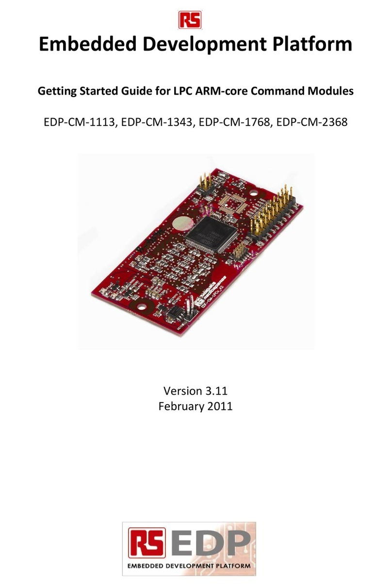
RS EDP-CM-PIM User manual

Embedded Development Platform
Getting Started Guide for Microchip PIM Carrier Module
EDP-CM-PIM
Version 3.11
February 2011

EDP-CM-PIM Getting Started V3.11
Electrocomponents plc Page 2
Contents
1. Introduction 3
2. Prepare to run the ‘Hello World’ Program 4
2.1 Software requirements.................................................................... 4
2.2 Hardware requirements................................................................... 4
2.3 Setting link Options......................................................................... 5
3. Run ‘Hello World’ 5
3.1 Load the Project.............................................................................. 6
3.2 Download and program target Flash memory ................................ 6
4. Build your own Project 6
4.1 Creating a new Project.................................................................... 6
5. Conclusion 6
6. Appendix 1 EDP I2C Bus Device Addresses 7

EDP-CM-PIM Getting Started V3.11
Electrocomponents plc Page 3
1. Introduction
To get the most out of the EDP platform it’s important to understand the concept of the EDP system
correctly. This is detailed in the user manual for the Base Boards which can be downloaded as a pdf
file from the RS EDP website.
RS EDP-BB-SystemBaseBoard User Manual Vx
The base boards come in both 2 position and 4 position formats and share a common user manual.
Please read this manual to get an understanding of the system.
Each of the Command Modules (CM) and Application Modules (AM) has its own user manual, so
again these documents must be read to get an understanding on how to use the modules.
Each of the boards comes with its own suite of software to fully exercise the EDP Application
Modules and the peripherals available on the MCU device.
An EDP system usually consists of one Command Module and one or more Applications Modules
plugged into a Base Board. A minimum system just has a Command module and Base Board, for
example a simple web server operating through an Ethernet connection.
The Command Module dictates whether the whole system uses a supply voltage of +3.3 or +5.0V.
This carrier module could have a PIM fitted which has a +5.0V or a +3.3V MCU on board. In this case
the dsPIC33FJ256 PIM module uses a +3.3V device and so the user should select this voltage first
using option jumper JP101 before applying power to the unit. The user can check the Vcc_CM signal
on the Base Board break-out header to confirm the system voltage.
There are 100 pins on the PIM and these are connected via various link options to the Base Board.
The Base Board then routes these signals to the Application Modules thereby allowing the PIM
Module to communicate with the Application Modules.
As many of the MCU pins have more than one function it can make the mapping of the connections
rather complex so there are additional support documents available to help you with this. The first is
the Pin Allocation Spread Sheet. The one for the Microchip PIM dsPIC33FJ256 module is called:
Pin Allocation - 100 pin PIM Module - dsPIC33FJ256MC710_Rev xx
This spreadsheet also forms part of the User Manual for the PIM Carrier module. It details which pins
are mapped to the Base Board backplane and the various link options which need to be configured to
connect them accordingly.
To get an appreciation of how the Application Modules are mapped to the backplane and how the
CPU Module can connect to them, a Mapping Aid exists. The one for the PIM carrier module is called:
Mapping Aid - dsPIC33FJ256MC710 Rev xx
This mapping aid also forms part of the User Manual for the PIM Carrier Module and at a glance you
can see what resources are required to get the best out of each Application Module.
Other useful documents you will need are the circuit diagrams for the modules you wish to use.
These are contained in the back of each user manual.
So before you start to use the RS EDP system make sure you have to hand the following documents:
Base Board User Manual
Appropriate CM module User Manual
Application Module User Manuals (as required)
EDP-CM-PIM Getting Started V3.11
Electrocomponents plc Page 4
2. Prepare to run the ‘Hello World’ Program
Program development is performed on a PC running suitable software, with a hardware
programming /debug interface between the PC and the PIM carrier module.
2.1 Software requirements
To build, download and run your first program you will need to have a suitable Integrated
Development Environment (IDE) running on a PC. Microchip provide a comprehensive free-to-
download IDE for all their MCU products called MPLAB. Download the latest version of MPLAB from
the Microchip web site and install it on your PC. The IDE handles all aspects of code production as it
contains a source code editor, Flash programmer and debug tools.
Also required is a terminal emulation program for the PC. Windows HyperTerminal is just about
suitable, but one of the free third-party programs such as TeraTerm is recommended.
2.2 Hardware requirements
The minimum EDP components needed to run the ‘Hello World’ project are: a BaseBoard, an EDP-
CM-PIM carrier module with a Microchip dsPIC33FJ256GP710 PIM (RS Stock No. 564-002) fitted and
an EDP-AM-CO1 communications module. The EDP will require a +12V power supply.
The PIM carrier module is fitted with an RJ-11 socket to take a connection to Microchip REAL ICE,
ICD2 or ICD3 hardware programming / debug interfaces. You will need one of these to program and
debug the PIM module.
The ‘Hello World’ test program sends a text message to a terminal display via the RS-232 ASC0
connector (J305) on the EDP Communications module. If your PC has a D-type COM socket then all
that is needed is a suitable cable. If not, then an RS-232 to USB converter cable will be needed to
connect the EDP to a spare USB port.
Note position
of pin 1 on PIM
Supply voltage
jumper link
Connection to
programmer

EDP-CM-PIM Getting Started V3.11
Electrocomponents plc Page 5
2.3 Setting link Options
The PIC PIM adapter board has a series of link options which allow the debug interface to be
connected to a variety of pins. This allows for flexibility in the choice of debug port and helps in some
cases free up other pins which can be used in the application. The PIM carrier User Manual describes
in detail how the emulation jumpers should be arranged and how the software for the fuse options
needs to be configured. The fuse options for the dsPIC for example, determine which of the debug
pins on the MCU are active.
The picture above shows the default jumper settings for the dsPIC33FJ256GP710 PIM Module and
the software that is provided. If you use a different PIM module other than the one shown, you will
have to determine which of the jumpers are relevant and set the fuse options in your software
accordingly if appropriate.
3. Run ‘Hello World’
The ‘Hello World’ project files are located in a compressed folder, EDP PIM Hello World, which may
be downloaded onto the host PC from the RS EDP or DesignSpark web sites.
Program target
Build project

EDP-CM-PIM Getting Started V3.11
Electrocomponents plc Page 6
3.1 Load the Project
Make all the connections between the EDP, interface module and the host PC and power up.
On the host PC run the terminal emulator, select the required serial port and set it up for
115200 baud, 8 data bits, one stop bit, no parity.
Run MPLAB on the host PC.
Select Project on the menu and click on Open…
Navigate to the EDP PIM Hello World folder and double-click on the EDP Hello World project
file (.mcp).
Make sure the Release mode is selected and not Debug on MPLAB.
3.2 Download and program target Flash memory
Select Programmer on the menu, then Select Programmer and then MPLAB ICD 3 (or
whatever tool you are using).
Click the programmer button to download the binary file into the target processor’s Flash
memory.
After programming, the code will execute. Pressing the EDP baseboard Reset button will re-
run the program.
If all has gone correctly, once the program execution has started, a message will appear in the
terminal emulator window.
4. Build your own Project
The MPLAB IDE contains an editor for producing source files, but a Compiler will need to be added to
produce code suitable for downloading to the target processor. A suitable C Compiler for the dsPIC
family, C30, can be downloaded from the Microchip web site in full, limited-trial or free limited-
function form. The latter is good for most simple projects. Obviously you will need a different
compiler for PIC32 or PIC24 PIM modules.
4.1 Creating a new Project
Create a project folder on your PC using Windows Explorer. Copy required driver files (source
and header) into the folder, along with the Main program file if the latter has been created
outside the IDE.
Run MPLAB.
Select Project on the menu and click on New…
Browse to the project folder, and type in a new project name.
Select Configure from the menu and click on Select Device….
Select a device from the list. It is important that this setting matches the PIM module so that
the Programmer uses the correct supply voltage.
Make sure the Release mode is selected and not Debug on MPLAB.
If all the source and header files are ready then click on the Build All button.
5. Conclusion
The example files and drivers provided are designed for the dsPIC33 series of processors.
Appropriate drivers will need to be obtained for other processor families such as PIC24 and PIC32.

EDP-CM-PIM Getting Started V3.11
Electrocomponents plc Page 7
6. Appendix 1 EDP I2C Bus Device Addresses
8-bit address format is used: the LSB is reserved as the read-write bit. These addresses are defined in
file: I2C-Directory.h
BaseBoard
BB_DIP = 0x40
8-bit DIP Switch
Address set by jumper link JP501 providing possible range of addresses: 0x40 (default), 0x42.
BB_EEPROM = 0xA2
Serial 4KB EEPROM memory
Address set by jumper links J601 to J603 providing possible range of addresses: 0xA0, 0xA2
(default), 0xA4, 0xA6, 0xA8, 0xAA, 0xAC, 0xAE.
Communications Module EDP-AM-CO1
CO1_RTC = 0xA0
Real-Time Clock and SRAM
Address set by jumper link J304 providing possible range of addresses: 0xA0 (default), 0xA2.
Digital I/O Module EDP-AM-DIO54
DIO54_Out = 0x46
Digital output latch
Address set by jumper links B305 to B307 providing possible range of addresses: 0x40, 0x42,
0x44, 0x46 (default), 0x48, 0x4A, 0x4C, 0x4E.
DIO54_In = 0x44
Digital input latch
Address set by jumper links B302 to B304 providing possible range of addresses: 0x40, 0x42,
0x44 (default), 0x46, 0x48, 0x4A, 0x4C, 0x4E.
Analogue Input Module EDP-AM-AN16
AN16_ADC = 0x6A
12-channel 10-bit Analogue to Digital Converter
AN16_Pot = 0x58
Digital Potentiometer for setting filter cut-off frequency of channels AN0 and AN1
Address set by jumper links J305 & J306 providing possible range of addresses: 0x58
(default), 0x5A, 0x5C, 0x5E.
Note that jumper links J204 & J205 select between CTRL_I2C (default) and I2C_GEN0 bus channels.
Dual BLDC Motor Module EDP-AM-MC2
MICROCHIP_MOTOR_DRIVER_BASE = 0x80
dsPIC U201
Address set by jumper links J201 to J203 providing possible range of addresses: 0x80
(default), 0x82, 0x84, 0x86, 0x88, 0x8A, 0x8C, 0x8E.
dsPIC U202
Address set by jumper links J205 to J207 providing possible range of addresses: 0x80, 0x82
(default), 0x84, 0x86, 0x88, 0x8A, 0x8C, 0x8E.
Note that spare addresses allow up to four MC2 modules per base board
Miscellaneous
SRF08 = 0xE0
Daventech SRF08 Ultrasonic Rangefinder module
Table of contents
Other RS Control Unit manuals
Popular Control Unit manuals by other brands

NXP Semiconductors
NXP Semiconductors TWR-K64F120M user guide

Fike
Fike TWINFLEX IRM 100-0011 Engineering and Commissioning Manual

Helo
Helo T2 Installation and user manual

Reznor
Reznor REC Series Installation operation & maintenance

Giacomini
Giacomini R453HY011 Instruction

Balluff
Balluff BNI IOL-302-S02-Z012-C11 user guide

Digi
Digi XBee product manual

Vexve
Vexve TERMOVAR Series Mounting and operating instructions

Kuhse
Kuhse KEA 291 NSTR operating instructions

Pilz
Pilz PIT gb Series operating manual

Radio Shack
Radio Shack Color Graphics Option installation instructions

GRASS VALLEY
GRASS VALLEY KAMELEON Series instruction manual