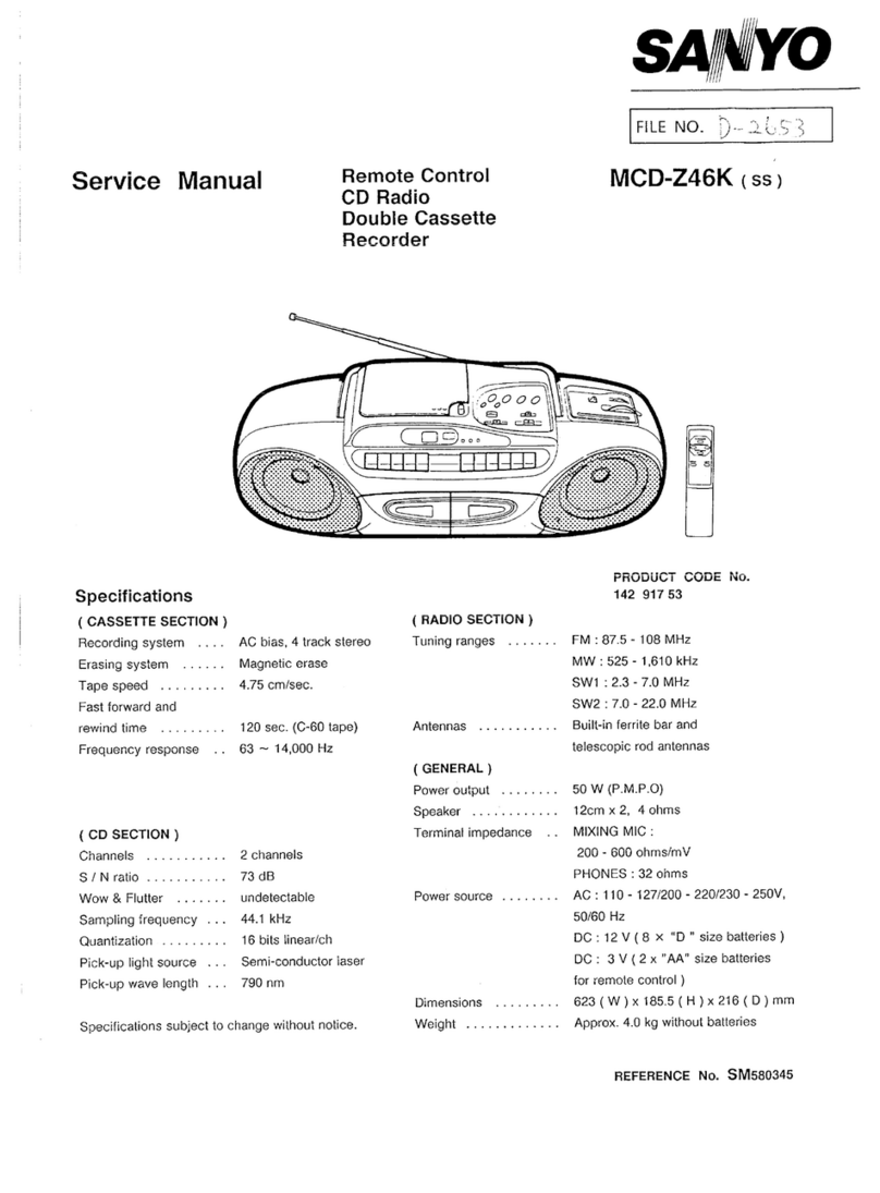
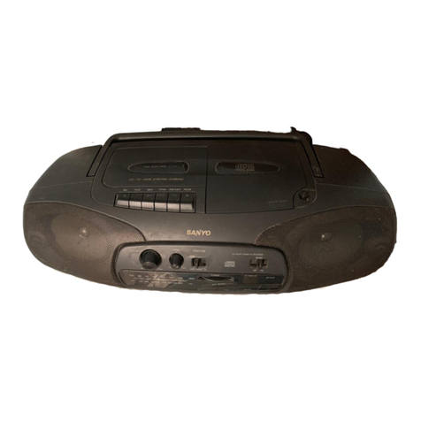
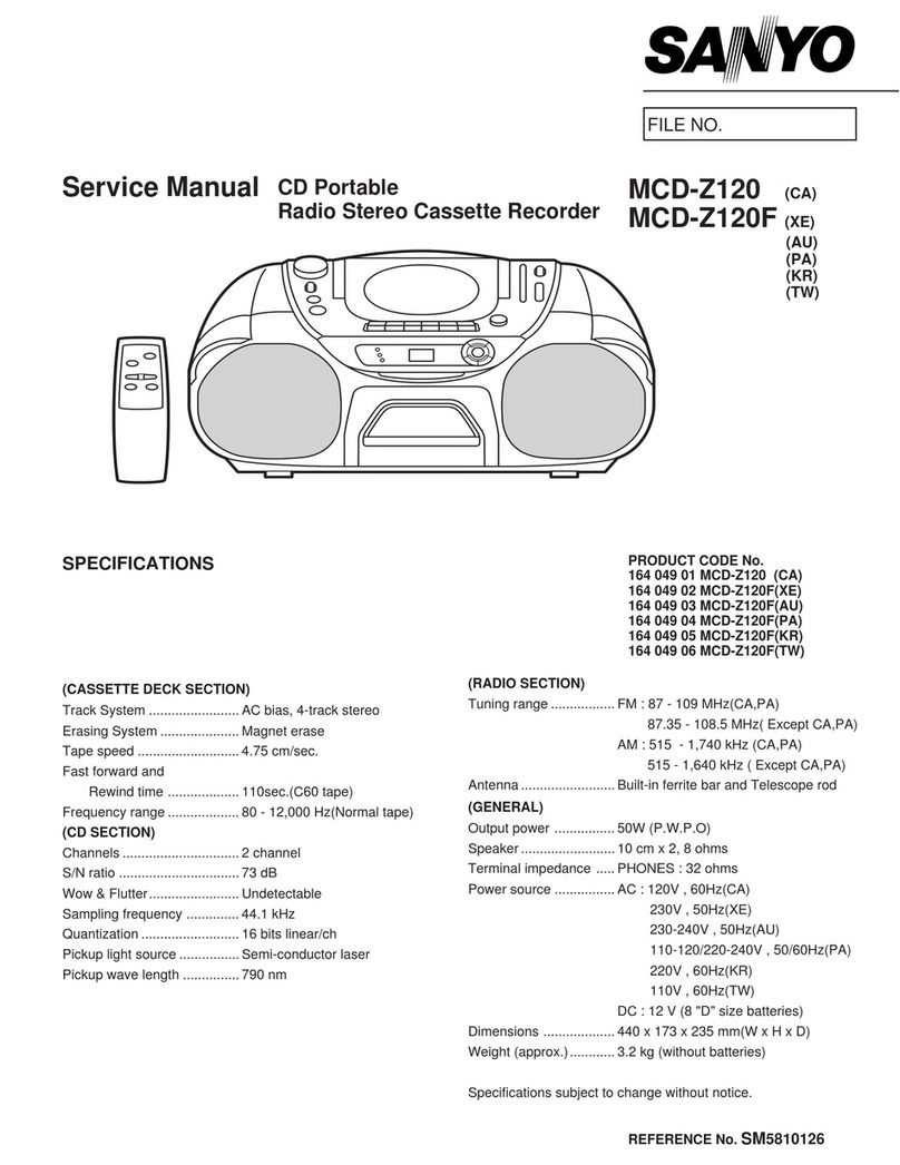
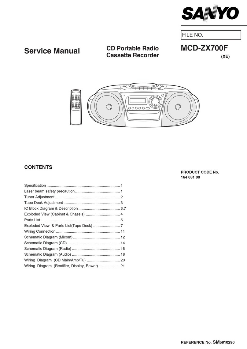
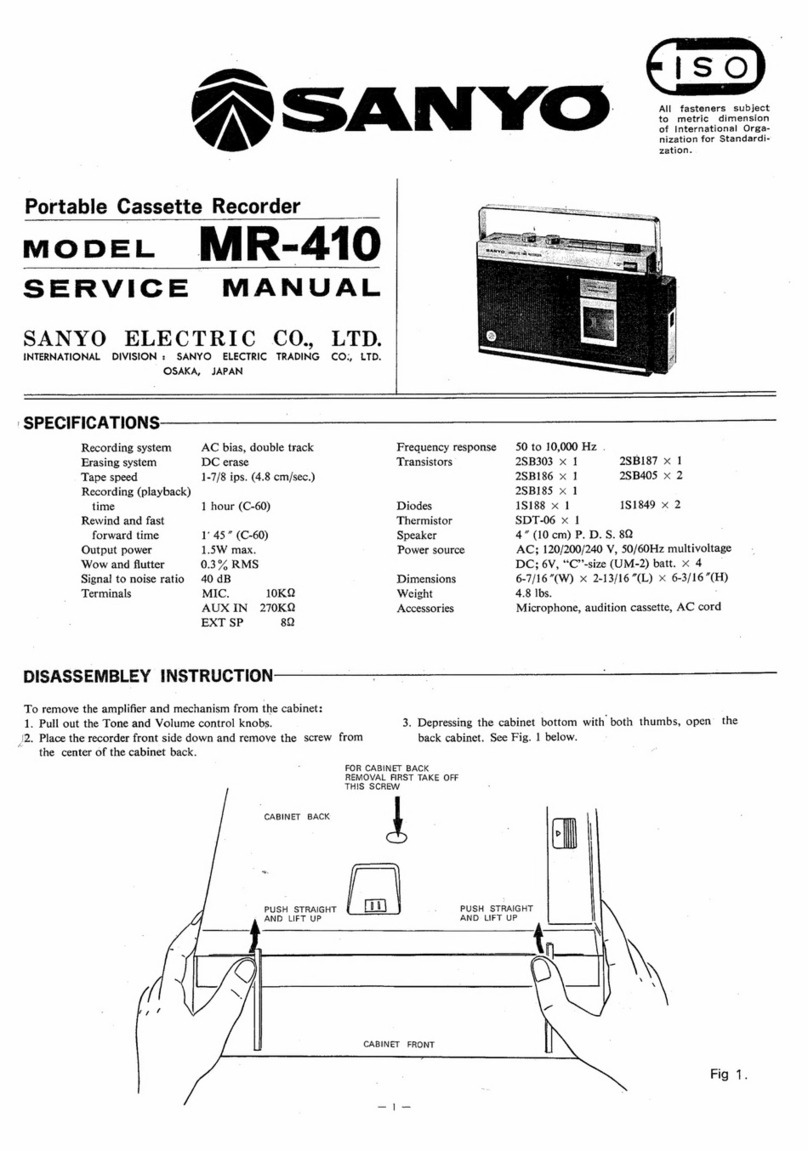
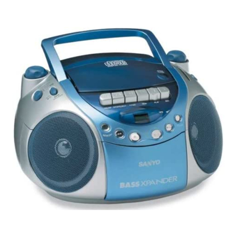
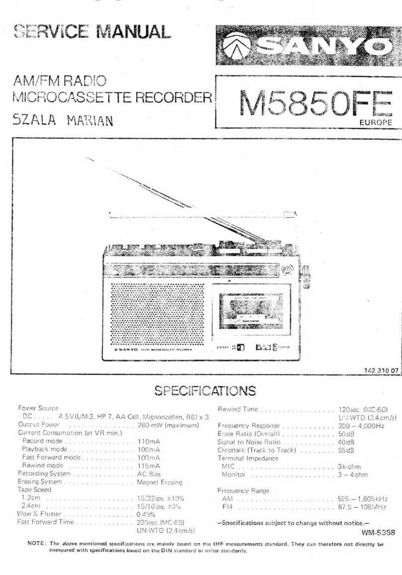
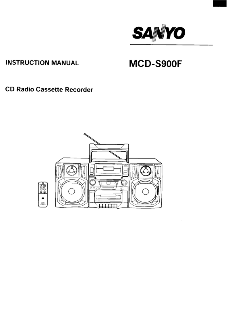
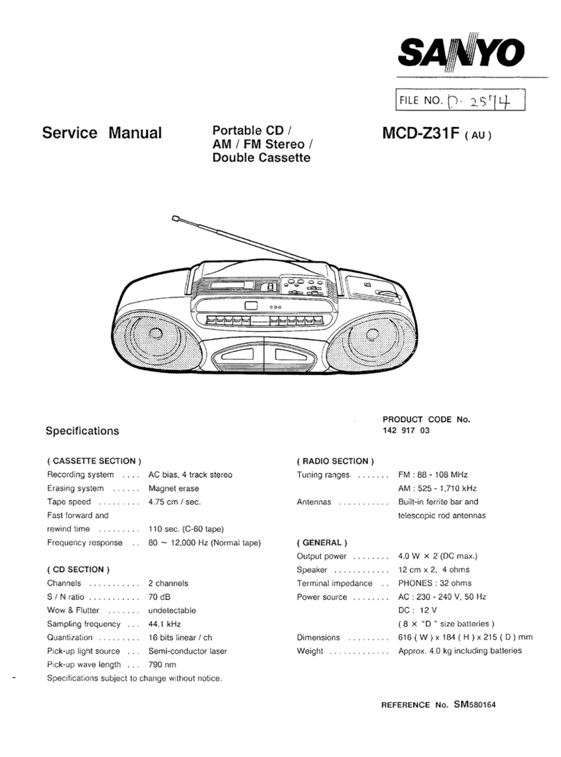
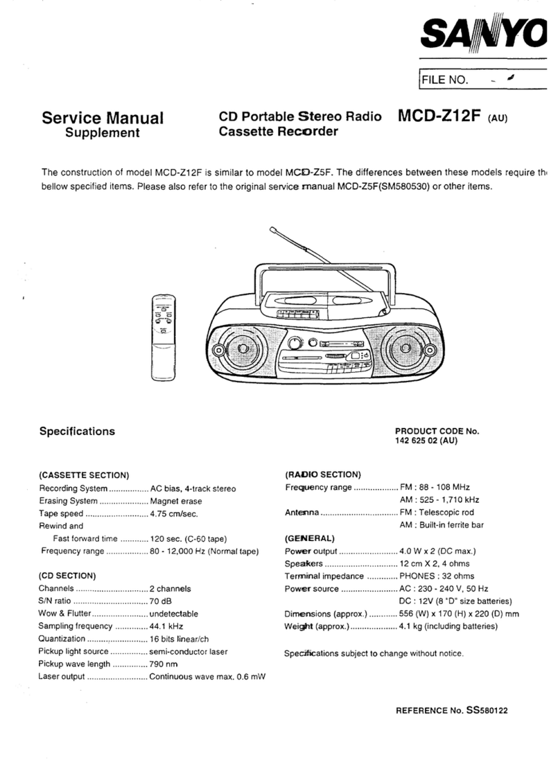
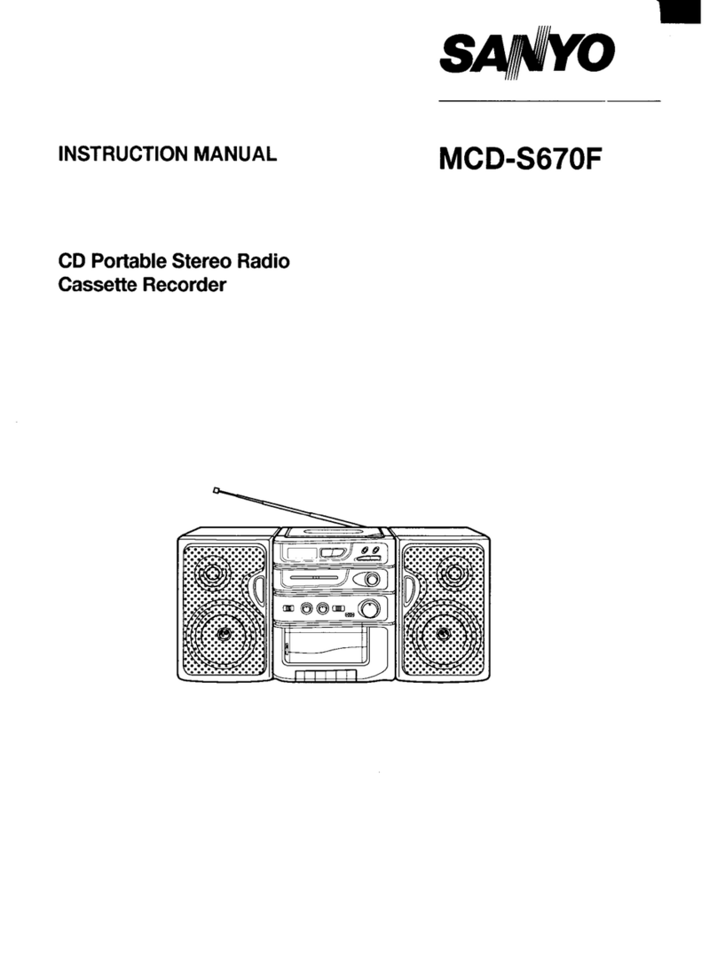
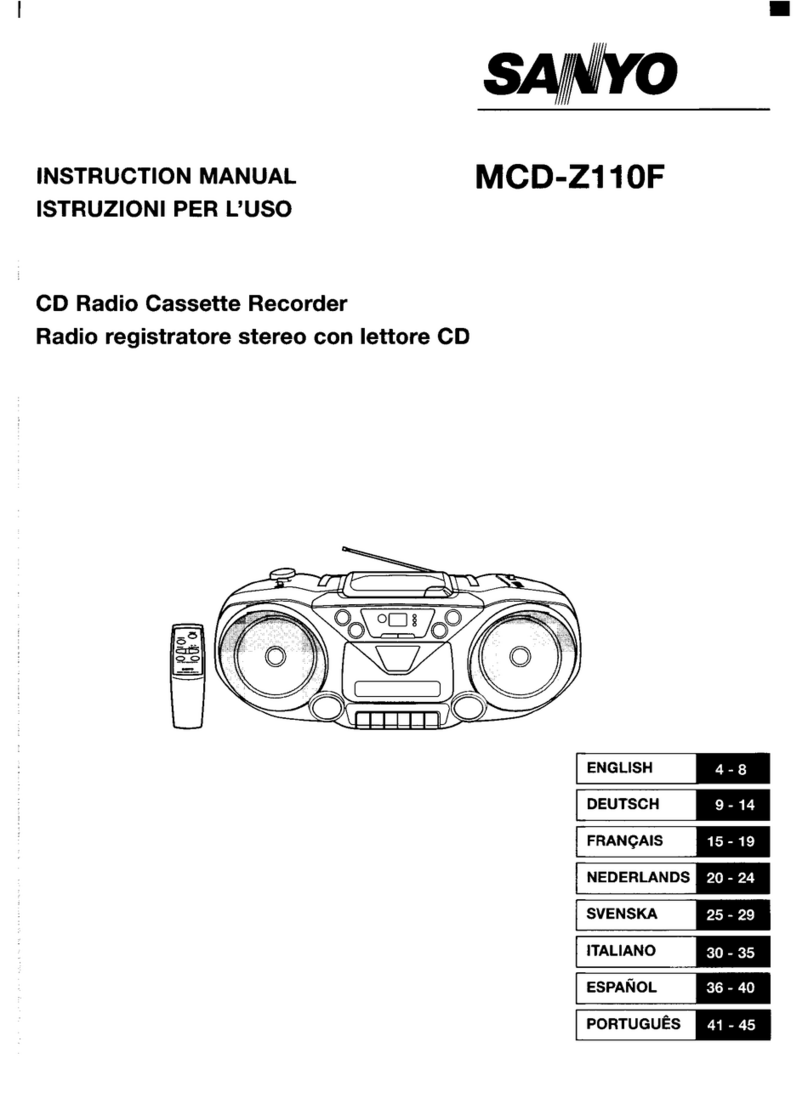
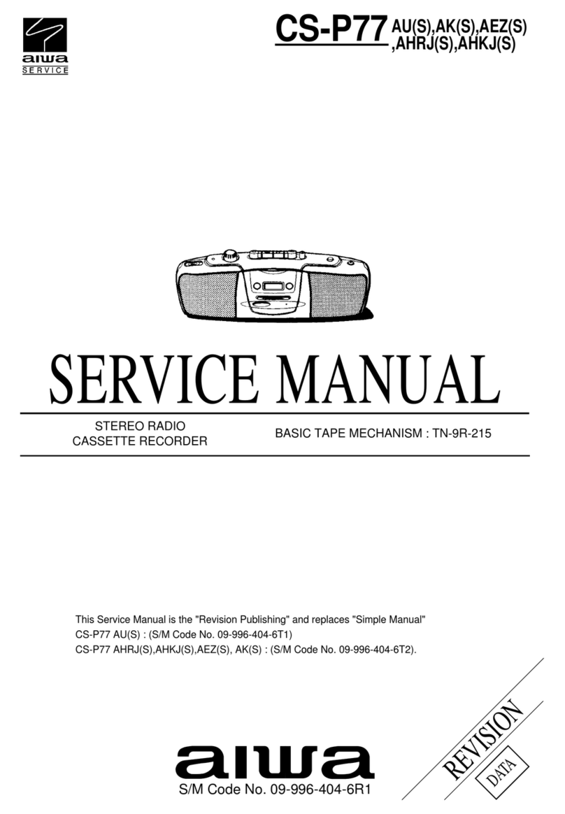
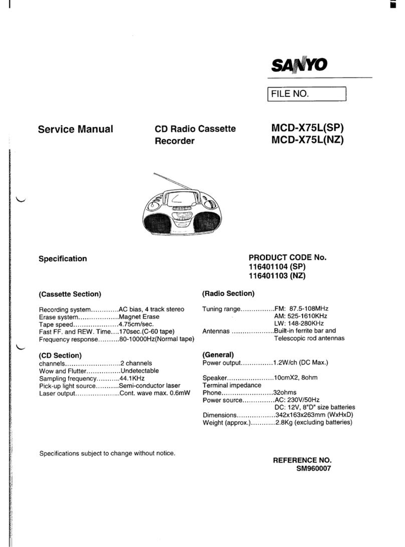
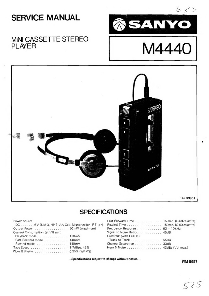
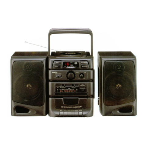
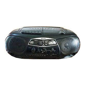
Sanyo MCD-S870F User manual

IFILE No. I
Service Manual
--
Specifications
CD Portable Stereo Radio MCD-S870F (AU)
Double Cassette Recorder
#
wl~ [[l,,,, I[[I I I~piii A
(CASSETTE SECTION)
Recording System .................AC bias, 4track stereo
Erasing System .....................Magnet erase
Tape speed ...........................4.75 cm/sec.
Fast forward and
rewind time ..........110 sec. (C-60 tape)
Frequency response .............63-14.000 t-iz
(CD SECTION)
Channel .................................2 channel
S/N ratio ..............................73 dB
Wow &Flutter ........................ Undetectable
Sampling frequency ..............44.1 kHz
Quantization . ..... .................16 bits linear/ ch
Pickup light source ................Semi-conductor laser
Pickup wave length ...............790 nm
Laser output ..........................Continuous wave max. 0.6 mW
PRODUCT CODE No.
14298302
(RADIO SECTION)
Tuning range .........................AM :525-1,710 kHz
FM:88-108 MHZ
Antenna ................................. FM :Telescopic rod
AM :Built-in ferrite bar
(GENERAL)
Power output .........................4.0 Wx2(DC max.)
Speaker ................................. 12 cm x2, 4ohms
PIEZO X2
Terminal impedance ............. PHONES :32 ohms
Power source ........................AC :230- 240V, 50 Hz
DC :12V (8”D” size batteries)
Dimensions ...........................670x280 x220mm(Wx HxD)
Weight (approx.) ....................7.4 kg (without batteries)
Specifications subject to change without notice,
REFERENCE No. SM580498

LASER BEAM SAFETY PRECAUTIONS
CAUTION :
USE OF CONTROLS OR ADJUSTMENTS OR
PERFORMANCE .OF PROCEDURES OTHER
THAN THOSE SPECIFIEDHEREIN MAY RE-
SULT IN HAZARDOUS RADIATION EXPO-
SURE
LASER OUTPUT ........0.6mW Max. (CW)
WAVELENGTH ...........790nm
●Pick-up that emits alaser beam is used in this CD player.
wv—
REMOVAL AND INSTALLATION
I
cAuTiON -INVISIBLE LASER RADIATION WHEN OPEN ..0
,.,,!?, “.., DEFEATED AVOID EX=OSURE TO BEAM
T-A
A.D”ARSEL USYNLIG MSER STRALING VEO ABNING, NAM
SIKKERHEDSAFBRY DERE ER UDE AF FUNKTION, UN CGA UDS ETTELSE FOR
vARNING OSYNLIG L4SER STRALNING NAR OENNA DEL AR OPPNAD
OCH SPARR AR URKOPPMD STRALEN AR FARLIG
vORSICHT -UNSICHTBARE LASERSTR AH LUNG TRITT AUS, WENN
DECKEL GEOFFNET uNO WENN SICHERHEITSVERRI EGELUNG
UBENBRUCIO IST NICHT DEM STRAHL AussET2EN
“..0 AVATTP. ESSA JA S“OML”KITUS OH ITETTAESSA OLET ALTTI INA
Nwimm5mLLE MSERSATEILYLLE ALP KA7S0 SATEESEEN I
.Remove the compact disc and cassette tape if there should be one on the disc tray or in the cassette lid.
●switch the power OFF, and unplug the AC power cord fron an AC outlet.
●AIIwiring should be returned to the original position after work is completed.
●First have ready many the new FIXERS (614 129 4971) for replacement.
●Arrange the lead wires so that they are not near the heat sink.
.Repair the (+)screwdriver more than 17 cm.
1. FRONT CABINET AND REAR CABINET
(1) Remove the battery lid.
(2) Remove the 7rear cabinet mounting screws. (})
2. TUNER BLOCK
2
,,,/’1. ~
,.
-1-

—
REMOVAL AND INSTALLATION
3. POINTER SETTING
111 POINTER
4. CD BLOCK
5. TAPE MECHANISM
-2-

TUNER ADJUSTMENTS
●Use aplastic screw driver for adjustments.
.Adjust the intermediate frequency of AM and FM to the frequency of ceramic filter.
Supply voltage :DC12.OV
Speaker impedance
Standard output
Function switch
BASS MID TREBLE
4ohm
50 mW (450 mV)
RADIO
Center L2005
PARTS LOCATION L2101
&VCT-1 VCT-3
VCT-2
~210*’ \J
mK
N“
XF213
J2116
Cl
J2118c
1C201 ~
@) PIN
1C2106”” Jxa
ADJUSTMENT BAND SELECT SWITCH :AM
Step Adjusting
Circuit
Connections SG Frequency Position of tuning dial Adjustment VTVM
Input Ootput Oscilloscope
Closed the output Connect sweep
terminal by sweep generator to C2106
generator, it place to (H)& J2108 (G) 455 kHz Low XF213 -4
L2005.
Connect AMSG to Connect VTVM to 517 kHz Low end L2008 Max.
Test Loop speaker terminals 1750 kHz High end VCT -4
$
1IF
2Tuning
3coverage
4Tracking
5
Connect AMSG to Connect VTVM to 600 kHz 600 kHz L2005 Max.
Test Loop speaker terminals 1400 kHz 1400 kHz VCT -3
I6IRepeatadjustrnents
2. FM ADJUSTMENT BAND SELECT SWITCH :FM
Adjusting Connections
Step SG Frequency
Circuit Input Ootput
VTVM
Oscilloscope
Position of tuning dial
Low
Adjustment
connect sweep 9en- Connect sweep gen-
1IF eratorto IC201 0eratorto C2106 (H) 10.7 MHz
(H) &J2118 (G) &J2108 (G)
A
...
4
2Connect FM SG to
Tuning Connect VTVM to
+
87 MHz
J2116 (H)
3coverage speaker terminals
&J2118 (G) 109 MHz
Low end L2102
VCT -2
Max.
High end
4Connect FM SG to Connect VTVM to 90 MHz
Tracking J2116 (H)
5speaker terminals
&J2118 (G) 106 MHz
6Repeat adjustments
L2101
VCT -1
90 MHz
106 MHz
Max.
I
-3-

TAPE DECK ADJUSTMENTS
1. HEAD REPLACEMENT 4. MOTOR AND BELT REPLACEMENT
.
●
●
●
●
Be sure to clean the heads before attempting to make any
adjustments.
After replacement, demagnetize the heads by using ade-
gausser.
All wiring should be returned to the original position after
work is completed.
After completion of the adjustment, use thread lock (TB-
1401 B) to secure the azimuth adjustment screws.
—
2. HEAD AZIMUTH ADJUSTMENT
●Be sure both channels (1 and 2) are the same level (Using
adual-channel oscilloscope).
.After completion of the adjustment, use thread lock (TB-
1401 B) to secure the azimuth adjustment screws.
(1) Insert the test tape (VTT-703, etc. :10 kHz) for azimuth ad-
justment into tape TAPE A.
(2) Press tape TAPE A’s PLAY button.
(3) Use across-tip screwdriver to turn the screw for adjust-
ment of the tape TAPE Aazimuth so that the left and riaht
outputs are maximized while tape TAPE
(4) Press the tape TAPE A’s STOP button.
(5) Repeat procedure for tape TAPE B.
3. MOTOR SPEED ADJUSTMENT
Ais playing back.
(I)lnsert the test tape (MTT-111 N, etc., 3000 Hz).
(2) Press the PLAY button.
(3) Ajust the VR405 so that the frequency counter becomes
3,000 Hz.
f-
v
5. CHECKING THE MECHANISM TORQUES AND TENSION
●Clean the head, capstan and pinch roller before making any measurement.
I
IMeasurement ITake-up torque IBack tension ITa~e tension 1
Cassette for PLAY:TW-2111 APLAY:TW-2111 ADrive-power cassette
measurement F. FWD/REW:TW-2231 TW-2412
PLAY 30- 60 gr.cm 2.0- 4.5 gr.cm 60 gr or more
F,FWD 55- 120 gr.cm ..- ---
REW 55- 120 gr.cm --- ---
-4-

REPLACEMENT OF CD MECHANISM
●Note that the mechanism of the CD player is very delicate.
●It is very important that the spindle motor (which rotates the disc), and the sled motor (which cases the disc signals to be
tracked), as well as the gear and other components, operate smoothly, without eccelentricity.
●When harldlirlgthepickup, take care not to exert excessive force, and particular care should be taken not to touch the lens
or the drive circuit’s P. W. Board pattern.
1. Replacement of the spindle motor
●First, prepare the new turntable (CM3-2) and new special
washer (CM3-4) for replacement. CM3-2
The removed turntable will be deformed by the heat of the
soldering iron, and cannot be reused.
●Prepare dial type calipers.
(1)The attached bonding material can be dissolved by using a
60 Wsoldering iron to heat the shaft at the under part of
the turntable (CM3-2) for about one minute.
~l##& -
(2) The turntable can then be removed from the shaft by very ----
carefully applying torte upward at the center of the lower
surface of the turntable.
(3) Remove the two screws (CM3-3) and remove the spindle
motor (CM3-5).
(4) Attach the special washer (CM3-4) to the spindle motor.
(5) Apply asmall amount of amixture of the “Three Bond
2001 and 201 5F” bonding materials to the motor’s shaft.
(6) Initial the turntable as shown in the figure. Secure the turn-
table by pressing gently. Be sure to wipe away (by using a
price of cloth, or similar material) any bonding material
coming out of the hole.
Don’t attached bonding mater Ial
at the top of shaft
IunIR110
+Olrnm
\CM2
(SHAFT)
Iu u J
Be sure to wipe away
the bonding mater!al
\CH~CK PUL.LEV
—1 ~J-
CM3-2
(TuRN
TABLE)—CM3-5
](sP]NDLE
MOTOR SHAFT )
2. Confirm of inclination for the turntable
(1) Connect the digital voltmeter as shown in the. figure
(2) Set the test disc (YEDS 18 =SONY or etc.), press the
PLAY button (Playback for the most inner music). F+ +
(3)At this time, record voltage value to indicate at the digital .
voltmeter. 10 kohm
Unit Digital
(4) Access the most outer music, press the PLAY button 0.0033PF Voltmeter
(Playback for the most outer music).
(5) Again at this time, record voltage value to indicate at the Vc
digital voltmeter. Low Pass Filter
(6) For reference at the recorded voltage of the most inner
music, Confirm at f300 mV less than for recorded voltage
of the most outer music
-5-
REPLACEMENT OF CD MECHANISM
.- 3. Replacement and lubrication of the pickup
●Before replacement of the pickup, be sure to carefully read
the section regarding the pickup when the unit is moved or
transported.
(1) Remove the apickup rail (CM2) with care fixing the latch
with way driver from bottom part of chassis (CM3-1 ).
(2) The pickup (CM9) can now be remove once the apickup
rail (CM2) have been taken out.
●When removing or inserting the apickup rail from or into
chassis, take care not to exert excessive force.
●If the pickup is reconditioned of replaced, be sure to wipe
the rails clean and also apply acoating of FLOIL (G-474B)
to there entire circumference and entire length. When ap-
plying the grease, do not allow any grease to adhere to
any other parts.
(3) Pass the apickup rail (CM2) through the new pick up
(CM9).
●The pickup P. W. Board pattern is “shorted”, as shown in
the figure, so that the new pickup will not be susceptible
to the effects of static.
●Set the pattern to “’open” after the pickup has been re-
placed.
‘“v! J:c”
SHORT
4. Checking the action of the CD mechanism 5. Replacement of the sled motor
(1) Disconn~ct the socket (for the sled motor power supply) (1) Remove the two screw (CYI )and remove the sled motor
. .from the P. W. Board. (CM5).
(2) APPIY avoltage of DC 2.0 Vto the sled motor’s terminal.
(3) Measure the current during sled motor operation.
●The direction of movement of the pickup (outer groove or
inner groove) can changed by changing the battery polar-
ity.
(4) The current during sled motor action varies according to CM3-1
the positional relationshiping of gears (CM7 and CM8).
(5) If the current exceeds 40 mA, remove the gears (CM7 and
CM8).
(6) APPIY asmall amount of aFLOIL (G-474B) bonding materi-
als to the chassis shafts.
-6-

REPLACEMENT OF CD MECHANISM
6. Resetting the pickup to the home position
(1) The limit switch is switched ON by the projection of this
rack gear secured to the returned pickup, after which the
sled motor continues to operate (by the circuit )for ap-
proximately 30 msec. :there is then again areverse opera-
tion, and movement to the position at which the switch is
switched OFF.
(2) Rotation continues for about 30 msec. after the switch is
switched OFF, and then the pickup stop at home position.
(
CONFIRM OF CD SECTION
1. Preparation
●Measuring instruments and Test disc.
(I)TEST DISC :YEDS 18 (SONY)
(2) OSCILLOSCOPE :SS5711 (10 MHz and Dual Phenomenon)
NOTE :CD section of this unit can not need adjustment, because CD Section P. W. Board checked at automatic checker.
2. Confirm of general operation
(l) Set the test disc.
(2) Press the PLAY button, then confirm the disc rotating to clockwise direction.
(3) Press the FFWD or REW button, then confirm the most inner music or most outer music accessing at speedy.
(4) Press the STOP button
CD Main and Display P.W. Board (Solder Side)
3. Confirm of eye pattern
(1)
Connect an oscilloscope to pin 41 (RF) of [Cl 01 and VR
point.
(2) Set the test disc, press the PLAY button.
(3) Check to be sure that the “eye” pattern is at center of
waveform and that the diamond shape is clearly defined.
(4) Press the STOP button.
IC1OI PIN41 (RF)
o
OSCILLOSCOPE
o
VR POINT
D
-7-

ii
EXPLODED VIEW (CABINET &CHASSIS)
\‘ ,. \
-8-

i
PARTS LIST
PRODUCT SAFETY NOTICE
EACH PRECAUTION IN THIS MANUAL SHOULD BE FOLLOWED D~BING SERVICING. COMPONENTS IDENTIFIED WITH THE IEC
SYMBOL ~IN THE PARTS LIST AND THE SCHEMATIC DIAGRAM DESIGNATE COMPONENTS IN WHICH SAFETY CAN BE OF SPE-
CIAL SIGNIFICANCE. WHEN REPLACING ACOMPONENT IDENTIFIED &USE ONLY THE REPLACEMENT PARTS DESIGNATED, OR
PARTS WITH THE SAME RATINGS C)F RESISTANCE, WATTAGE OR VOLTAGE THAT ARE DESIGNATED IN THE PARTS LIST IN THIS
MANUAL. LEAKAGE-CURRENT OR RESISTANCE MEASUREMENTS MIUST BE MADE TO DETERMINE THAT EXPOSED PARTS ARE
ACCEPTABLY INSULATED FROM THE SUPPLY CIRCUIT BEFC)RE RETURNING THE PF?ODUCT TO THE CUSTOMER.
CAUTION :Regular type resistors and capacitors are not listed. To, know those values, refer to the schematic diagram.
Regular type resistors are less than l/4W carbon type and Oohm chip resistors.
Regular type capacitors are less than 50V and less than 1000pF type of Ceramic type and Electrical type.
N.S.P
‘ACKlb
Ref. No
:Not available as service parts.
i&ACCESSORIES
Part No.
614 271 6540
614 267 8480
614 267 8473
614 256 5674
614 271 6663
614 231 6832
645 009 6143
Lh614 25CJ 6578
~614 256 5292
CABINET &CHASSIS
r
Ref. No
1
2
3
14
5
6
17
,8
19
I::
~12
~13
i14
!15
16
17
18
19
20
21
22
23
24
25
31
32
33
34
35
36
37
38
39
40
Part No.
614 267 8213
614 267 5168
614 267 5175
614 271 6069
614 270 3250
614 267 5144
614 270 4226
614 267 4963
614 267 8299
614 263 4912
614 267 4567
614 267 4574
614 267 5090
614 267 4970
614 26? 4987
614 267 4994
614 267 5007
614 267 5014
614 267 5021
614 267 5038
614 267 5045
614 267 5052
614 267 5069
614 267 5076
614 267 5083
614 267 5250
614 248 2551
614 268 5716
614 244 8199
412 032 6408
614 25& 1544
614 247 6048
614 217 9291
412 032 6408
412 032 6408
Description
CARTON CASE
CUSHION,TOP
CUSHION,BOTTOM
SHEET,SET
INSTRUCTION MANUAL
LABEL,SAFETY,LASER CLASS
REMOCON.MCD-S870
POWER CORD,AC-IN
POWER CORD,AC-IN
Ref. No.
41
42
43
44
45
46
47
48
4Fi
50
51
Description
ASSY,CABINET,FRONT
LID,CASSETTE,TAPE B
LID,CASSETTE,TAPE A
ASSY,CABINET,REAR
HANDLE
LID,CD
LID,BATTERY
KNOB, ROTARY,TUNING
KNOB, ROTARY,VOLUME
KNOB,ROTARY,BASS.MIDOTREBLE
BUTTON,CD,OPEN
BUTTON,CD OPERATION
KNOB,SLIDE,FUNCTION
KNOB,LEVER,(B)REC
KNOB,LEVER,(B)PLAY
KNOB,LEVER,(B)REW
KNOB,LEVER,(B)FFW
KNOB,LEVER, (B)EJECT
KNOB,LEVER, (B)PAUSE
KNOB, LEVER,(A)MODE
KNOB, LEVER,(A)PLAY
KNOB,LEVER, (A)REW
KNOB,LEVER,(A)FFW
KNOB, LEVER,(A)EJECT
KNOB, LEVER, (A)DIRECTION
~ANEL.TOP
V3SY,PULLEY,CD CHUCKING
;PRING,WIRE,CD OPEN
LSSY,GEAR,CD OPEN DUMP
3CREW,SPECIAL,CD-DUMPER
$LIDE,CD OPEN
;USHION,CD MECHANISM
SPRING,COMP,CD MECHANISM
;CREW,SPECIAL,CD MECHANISM
jCREW,SPECIAL,CASSETTE-GEAR
!3’2
93
Part No.
614 268 6188
614 244 8199
614 225 1744
614 10B 2929
614 247 2941
614 267 5199
614 267 5229
614 267 5106
614 267 8282
614 267 4840
614 267 5281
614 267 5236
614 267 5274
614 268 5402
614 26B 5419
614 268 5426
%XINGPARTS
Ref. No,
YCJ1
Y02
YCt3
YL?4
Yll
Y12
Y13
Y14
Y21
Y2.2
Y2?3
Y.24
Y&i
Y2%
Part No.
411 021 4906
411 021 4104
411 002 9104
411 021 4906
411 020 8905
411 021 3503
411 021 4005
411 021 4005
411 025 2007
411 021 4005
411 022 2802
411 020 9100
411 021 4005
411 021 4005
411 021 4005
411 020 9100
411 020 9100
411 021 4005
411 098 7107
411 085 1200
Description
SPRING,WIRE,CASSETTE
ASSY,GEAR,CASSETTE OPEN DUPM
BRACKET-M,MECHA KNOB LEVER
BRACKET,R/P
SPRING,PLATE,R/P
LEVER,R/P
MOUNTING,TUNER
KNOB,LEVER,BAND
GEAR,VC,TUNER
GEAR,TUNER
SHAFT,TUNER
MOUNTING,SHAFT
POINTER
ASSY,BOX,FRONT, LEFT
ASSY,BOX, FRONT,RIGHT
ASSY,BOX,REAR
Description
SCR S-TPG BIN 3X20,CABI-REAR
SCR S-TPG BIN 3X12,PANEL TOP
SCR PAN 3X8,ROD ANT
SCR S-TPG BIN 3X20,
SPEAKER BOX(L)(R)
SCR S-TPG BRZ+FLG 3X1O,
SPEAKER(L)(R)
SCR S-TPG BIN 3X1O,
MECHA-BUTTON-BRACKET
SCR S-TPG BIN 3X12,CD PWB
SCR S-TPG BIN 3X12,
TAPE MECHANISM
SCR S-TPG PAN 2X4,R/P
SCR S-TPG BIN 3X12 R/P LEVER
SCR S-TPG FLT 3X10,R/P
SCR S-TPG BRZ+FLG 3X12,P.T
SCR S-TPG BIN 3X12,AC SOCKET
SCR S-TPG BIN 3X12,
MOUNTING TUNER
SCR S-TPG BIN 3X12,
MOUNTING SHAFT
SCR S-TPG BRZ+FLG 3X12,
BAND LEVER
SCR S-TPG BRZ+FLG 3X12,GEAR
SCR S-TPG BIN 3X12,TUNER PWB
BOLT HEX C-SCT 2.6X12,
VC-GEAR
WASHER OUT TW 2.6,VC-GEAR
-9-

i
PARTS LIST
ELECTF
Ref. No.
61
~r
52
63
64
65
66
67
68
69
TUNER
Ref. No.
31
:2101
:2107
:N201
)2001
1C201
.2005
)r
jr
.2008
.2101
Dr’
Dr
or
L2102
or
Q2102
or
Q2103
or
S2101
or
VC201
X2001
or
XF201
XF211
or
or
o.r
or
or
or
or
or
or
XF213
XF214
or
or
or
or
or
or
or
or
2AL PARTS
Part No. ~
h423 005 9500
h423 016 7809
A614 241 2435
645 011 0337
419 002 0206
614 258 1162
614 270 4301
614 270 4318
614 270 4325
614 270 4332
W. BOARDA:
=
Part No.
614 268 5495
403 154 2102
403 154 2102,
614 206 0216
407 012 4406
409 325 7006
614 272 6556
614 230 6888
614 254 9964
614 256 6572
614 034 7197
614 034 7203
614 225 1966
614 034 7210
614 035 0012
614 229 0217
405 017 9709
405 017 9600
405 CS17 9709
405 017 9600
614 244 8335
614 024 3185
614 253 6278
645 004 6100
645 009 5801
614 252 1045
614 030 5630
614 03(1 5647
614 030 5654
614 U30 5661
614 030 5678
645 010 0079
645 010 0086
645 010 0093
645 010 0109
645 010 0116
645 004 6094
614 253 6841
614 231 3145
614 231 3152
614 231 3169
614 231 3176
645 010 0123
645 010 0130
645 010 0147
645 010 0154
Description
FUSE,250V 2A,FU401
FUSE,250V 2A,FU401
ANTENNA,ROD,FM
SPEAKER,4,WOOFER,SP471 .SP481
PIEZO BUZZER 7MB-20-5R5,
TWEETER,SP472”SP482
CORD,2P,CONNECTOR,
CN471.CN481,SPEAKER
CORD,5P
coNNEcToR,cN430,R/P/E-HEAD
COR0,3P CONNECTOR,CN431,P-
HEAD
CORD,4P CONNECTOR,CN432,AMP-
MOTOR
CORD,8P CONNECTOR,CN433,AMP-
MECHA
;Y
Description
4SSY,PWB,TUNER
!P-ELECT lU M50V
YP-ELECT lU M50V
SOCKET,4P,T0 AMP
310DE 1SS133
IC TA8122AN
ASSY,BAR ANTENNA,AM
!ASSY,BAR ANTENNA,AM
ASSY,BAR ANTENNA,AM
TRANS,OSC,AM
VHF COIL,FM
VHF COIL,FM
VHF COIL,FM
VHF COIL,FM
VHF COIL,FM
VHF COIL,FM
TR 2SC3330-U
TR 2SC3330-T
TR 2SC3330-U
TR 2SC3330-T
SWITCH,SLIDE,BAND
SWITCH,SLIOE,BAND
VC(VARIABLE CAPACITOE)
OSC,CERAMIC 456KHZ
OSC,CERAMIC 456MHZ
FILTER,LC,FM,BAND PASS
IF FILTER,FM, 1O.7MHZ,REO
IF FILTER, FM,1O.7MHZ,BLUE
IF FILTER, FM, 1O.7MHZ,ORANGE
IF FILTER,FM,1O.7MHZ,BLACK
IF FILTER, FM,1O.7MHZ,WHITE
CERAMIC FILTER 10.7OMHZ
CERAMIC FILTER 10.67MHZ
CERAMIC FILTER 10.73MHZ
CERAMIC FILTER 10,64MHZ
CERAMIC FILTER 10.76MHZ
CERAMIC FILTER 455KHZ
RESONATOR,CERAM, 1O.7OMHZ
RESONATOR,XTAL, 10,67MHZ
RESONATOR,XTAL, 10.73MHZ
RESONATOR,XTAL, 10.64MHZ
RESONATOR,XTAL, 10.76MHZ
OISCR,CERAMIC 10.7OMHZ
DISCR,CERAMIC 10.67MHZ
DISCR,CERAMIC 10.73MHZ
DISCR,CERAMIC 10.64MHZ
ML No. Part No. Description
)r I645 010 0161 DISCR,CERAMIC 10.76MHZ
DMAI
Ref. No.
Iz
:1401
:Mlol
;F4102
:N’103
)r
:Bllo4
>r-
:MI07
)r-
:MI08
Jr
)1501
38-
11507
>F
Iclol
ICI02
ICI03
ICI04
ICI05
L1451
PR102
Q1301
Qfr
ori-
Q1401
or
01.403
or
or
Qli404
Gr
o&-
;;501
or
or
;;502
06-
o&-
::505
or
or
&06
QB781
Q1782
QIX881
Q3882
X1451
XZ501
P.W.130ARDASSY
Part No.
614 271 7417
403 135 3302
645 010 1465
645 005 8127
614 035 4911
614 237 9752
645 012 2750
614 231 2759
614 Z54 3597
614 221 8273
614 254 3597
614 221 8273
407 007 9904
407 012 4406
407 007 9904
407 012 4406
409 346 2806
409 331 4006
~409 317 8509
409 329 4209
410 234 4505
614 028 6748
645 006 2322
405 007 6701
405 006 4005
405 006-3909
A405 009 5207
~405 001 9302
405 007 6701
405 006 4005
405 006 3909
405 018 2600
405 000 4407
405 078 2800
405 001 0309
405 066 9507
405 000 3400
405 078 2008
405 107 8704
405 000 4407
405 078 2800
405 001 0309
405 018 2600
405 018 2600
405 000 4407
405 078 2800
405 001 0309
405 000 1604
405 075 8409
405 075 8409
405 075 8409
405 075 840S
614 231 2667
614 215 557E
Description
LSSY,PWB,CD MAIN
;LECT 1000U M6.3V
;OCKET,FPC 13P,T0 PICKUP
‘LUG,6P,T0 CD MECHANISM
;OCKET,2P,T0 OPEN/CLOSE
;OCKET,1OP,TO AMP
11P MATE SOCKET,1OP
rERMINAL,lP,TEST POINT
FERMINAL,lP,TEST POINT
GERMINAL, lP,TEST POINT
FERMINAL,lP,TEST POINT
)IODE GMAO1
)IODE 1SS133
)IODE GMAO1
)IODE 1SS133
[C LA9220MS
[C LC7861KE
[C BA6398FP
[C UP06379GR
[C LC651104F-4F77
Sw
Sw
FILTER,1OUH,RIPPLE CANCEL
PROTECTOR,IC,0.4A 50V
TR 2SB598-F-NP
TR 2SA952-L
TR 2SA952-K
TR 2SB927-S
TR 2SA102O-Y
TR 2SB598-F-NP
TR 2SA952-L
TR 2SA952-K
TR 2SC3400
TR DTC124ES
TR BA1F4M
TR RN1203
TR 0TC143TS
TR DTC114TS
TR BA1L3Z
TR BA1A4Z
TR DTC124ES
TR BA1F4M
TR RN1203
TR 2SC3400
TR 2SC3400
TR DTC124ES
TR BA1F4M
TR RN1203
TR DTA143ES
TR DTC144TS
TR DTC144TS
TR DTC144TS
TR 0TC144TS
RESONATOR,CERAMIC, 16.93MHZ
RESONATOR,CERAMIC ,2.09MHZ
319DISPLAYP.W. BOARDASSY 1
*f. No. Part No. IDescription
83 I614 272 0158 lASSY,pWB,OISPLAy
ti3502 407 137 4206 LED SL-1255-05,
2-DIGIT 8-SEGMENT
-1o-

PARTS LIST
Ref. No.
or
D1503
D1504
D1505
D151O
Q1503
Q1504
S1501
S1502
S1503
S1504
S1505
S1506
Part No.
407 168 3605
408 017 5801
408 017 5801
408 017 5801
407 169 9408
405 OOil 1604
405 000 1604
614 240 1002
614 240 1002
614 240 1002
614 240 1002
614 240 1002
614 240 1002
Description
LED SL-1255-05,
2-DIGIT 8-SEGMENT
LED SLZ-981C-15-AB,PLAY
LED SLZ-981C-15-AB,REPEAT
LED SLZ-981C-15-AB,MEMORY
PHOTO DIOOE SPS-421-l-
A,IR(REMOCON) RECIVER
TR DTA143ES
TR DTA143ES
SWITCH,TACT,STO?
SWITCH,TACT,PLAY
SWITCH,TACT,UP
SWITCH,TACT,DOWN
SWITCH,TACT,REPEAT
SWITCH,TACT,MEMORY
CDOPEN/CLOSE SWITCH P.W. BOARD ASSY
Ref. No. Part No. Description
84 614 271 7400 ASSY,PWB,CO SWITCH
CN105 614 035 4911 SOCKET,2P,T0 CD MAIN
or 614 237 9752 SOCKET,2P,T0 CD MAIN
S1507 645 004 7787 SWITCH,LEVER lP-
2T,oPEN/cLosE
AMPLIFIER P.W. BOARDASSY
Ref. No,
85
C4732
C4734
C4832
C4834
C4921
C4922
C4930
CN401
CN402
CN403
:;405
CN406
CN407
CN408
CN41O
CN420
CN421
D4901
D4902
D4903
D4904
D4905
D4906
D4913
D4914
D4920
D4922
D4923
HS401
IC401
IC402
IC403
L4701
or
L4801
Part No.
614 272 0943
403 058 5308
403 125 5507
403 058 5308
403 125 5507
403 062 0306
403 058 9900
403 135 0400
614 206 0278
645 004 2904
614 035 4935
614 237 9776
645 004 2898
645 004 2928
645 005 8134
614 229 3812
645 004 2881
645 006 1875
645 006 1875
407 007 9904
407 007 9904
A407 053 8708
408 017 5405
408 017 5405
407 007 9904
407 140 7201
~407 053 8005
407 007 9904
~407 053 8302
A407 053 3109
614 249 0754
409 251 1000
Lh409 295 7402
409 114 4803
645 006 9864
614 212 3171
645 006 9864
Description
ASSY,PWB,MAIN AMP
POLYESTER 0.15U K50V
ELECT 1000U M16V
POLYESTER 0.15U K50V
ELECT 1000U M16V
POLYESTER 0.047U K50V
POLYESTER 0.018U K50V
ELECT 3300U M25V
SOCKET,1OP,TO CD MAIN
PLUG,4P,T0 MOTOR
SOCKET,4P,T0 TUNER
SOCKET,4P,T0 TUNER
PLUG,3P,T0 PHEAD
PLUG,6P,T0 R/P HEAD
PLUG,8P,T0 TAT. MECHANISM
JACK,HEADPHONE
PLUG,2P,T0 POWER SUPPLY
PLUG,2P,T0 SPEAKER
PLUG,2P,T0 SPEAKER
DIODE GMAO1
DIODE GMAO1
ZENER DIODE MTZ9.lA
LED SLZ-981C-13-AB-T2,DIRECT
DIODE GMAO1
DIOOE DSR-1OC-ET5
ZENER DIODE MTZ7.5B
DIODE GMAO1
ZENER DIODE MTZ8.2A
ZENER DIODE MTZ12A
HEAT SINK
IC TA8189N
IC TA8229K
IC LB1641
INDUCTOR,80U
INDUCTOR,80U
INDUCTOR,80U
R&f. No.
as-
L4901
L4902
L4903
LG401
LS402
Q4701
QJ3702
:’:703
:;801
Q4802
&803
mr
@1902
&903
&904
;905
c~906
;:910
;:91 1
w
Q4912
;913
a%-
csr
or
G914
c%r
R4737
!%4837
IW920
ii24940
F#4941
R4950
.%3901
S4902
%903
SJ1401
v13401
V3?402
b%?403
!m1404
VR405
P’C3WEfi
:RM?f. No.
85
c.l?i413
m414
w
CS416
FCL41
FK-C42
k4904
Part No.
614 212 3171
614 224 7983
645 011 6414
645 011 6414
614 217 7273
614 217 7273
405 OIB 2808
405 010 9706
405 010 9607
405 010 9706
405 010 9607
405 018 2808
405 010 9706
405 010 9607
405 010 9706
405 010 9607
405 017 9709
405 017 9600
~405 023 5306
Lh405 023 5009
405 004 5004
405 004 4502
405 017 9709
405 017 9600
405 017 9709
405 017 9600
405 017 9709
405 017 9600
405 004 5004
405 004 4502
405 017 9709
405 017 9600
A405 095 i602
A405 095 1701
h405 073 5202
LL405 C35 7107
~405 035 7206
405 023 5306
405 023 5009
402 071 1304
402 071 1304
~402 071 0307
~402 071 0208
~402 071 0307
402 071 4701
645 011 0368
614 247 8561
614 235 4506
411 021 6405
645 009 8710
645 011 0429
645 011 0429
645 011 0429
645 006 2537
Description
INDUCTOR,80U
TRANS,OSC,BIAS
INDUCTOR,lM J
INDUCTOR, IM J
LUG,LEAD WIRE FIX
LUG,LEAD WIRE FIX
TR 2SC3402
TR 2SC1571-G-NP
TR 2SC1571-F-NP
TR 2SC1571-G-NP
TR 2SC1571-F-NP
TR 2SC3402
TR 2SC1571-G-NP
TR 2SC1571-F-NP
TR 2SC1571-G-NP
TR 2SC1571-F-NP
TR 2SC3330-U
TR 2SC3330-T
TR 2SD400-F-MP
TR 2SD400-E-MP
TR 2SA608-G-NP
TR 2SA608-F-NP
TR 2SC3330-U
TR 2SC3330-T
TR 2SC3330-U
TR 2SC3330-T
TR 2SC3330-U
TR 2SC3330-T
TR 2SA608-G-NP
TR 2SA608-F-NP
TR 2SC3330-U
TR 2SC3330-T
TR 2S02061-E
TR 2SD2061-F
TR 2SD2012
TR 2SD1913-R
TR 2S01913-S
TR 2AD400-F-MP
TR 2AD400-E-MP
FUSIBLE RES 2.2 JA l/4W
FUSIBLE RES 10 JA l/4W
FUSIBLE RES 27 JA l/4W
FUSIBLE RES 10 JA l/4W
FUSIBLE RES 3.3 JA l/4W
SWITCH,SLIDE 4P-4T,FUNCTION
SWITCH,SLIDE,R/P
SWITCH,SLIDE,BEAT
SCR S-TPG BIN 3X8
VR,ROTARY,50KBX2 ,VOLUME
VR,ROTARY,1OOKBX2 ,BASS
VR,ROTARY 100KBX2,TREBLE
VR,ROTARY 100KBX2,MID
VR,SEMI,2K N,TAPE SPEED
;UPPLY P.W. BOARDASSY
Part No.
614 272 1018
614 020 1215
614 020 6548
614 223 9209
614 270 4349
~645 006 4760
~645 006 4760
/jJ645 006 8072
Description
ASSY,PWB,POWER SUPPLY
SOCKET,2P,T0 AMP
SOCKET,2P,T0 BATT
SOCKET,2P,T0 BATT
CORD,2P CONNECTOR,AMP-DG
HOLDER,FUSE
HOLDER,FUSE
INDUCTOR, 181U

ii
PARTS LIST
Ref. No. Part No. Description
T4901 ~614 271 8551 POWER TRANSFORMER
\c So(
Ref. No.
87
CN412
or
D4907
D4908
D4909
D491O
ET P. W. BOA
Part No.
614 272 0981
~614 020 7590
~645 005 7038
~407 098 3300
~407 098 3300
~407 098 33oO
Li1407 098 3300
DASSY
Description
ASSY,PWB,AC SOCKET
SOCKET,2P,AC IN
SOCKET,2P,AC IN
DIODE RL153-BF-S2
DIODE RL153-8F-S2
DIODE RL153-BF-S2
DIODE RL153-BF-S2
BATTERY TERMINAL P. W. BOARD ASSY
~
614 118 4036 TERM;NAL’BATTERY (-)
614 020 6548 SOCKET,2P,T0 POWER SUPPLY
614 223 9209 SOCKET,2P,T0 POWER SUPPLY
-12-

ii
EXPLODED VIEW (CD MECHANISM)
CY1— -
f~ CY1
.—— —-l —-l —— ————————— ——-l
II‘s1
I
I
I
I
I
I
,}
I
I
I
I
I
I
I
I
I
PARTS LIST (CD MECHANISM)
:D ME(
Ref. No.
CMI
CM2
CM3
CM4
CM5
CM6
CM7
CM8
CM9
CM1O
+ANISM (PM-C
Part No.
614 268 8069
614 237 7024
614 265 7874
614 262 2575
645 007 7821
614 245 4268
412 032 0208
411 044 7502
614 024 1778
645 007 7814
614 237 7093
614 237 7109
614 237 7116
645 006 7983
614 262 2599
‘BM94C1SH)
Description
ASSY,WIRE,MOTOR &SW
SHAFT,PICK UP RAIL
ASSY,CHASSIS,BASE MECHANISM
CHASSIS,BASE MECHANISM
MOTOR,SPINDLE,DC,0.2W
TURNTABLE,SPINDLE
WASHER,SPECIAL,ADHESIVE
ESCAPE STOP
SCR PAN+SW 2X5,SPINDLE MOTOR
FIX
SWITCH,LIMIT
ASSY,MOTOR,SLED
GEAR,SLED RETARD 1
GEAR,SLED RETARD 2
GEAR,SLED
PICKUP,LASER, F-P1OO
GEAR,RACK,PICK RACK
[
Ref. No.
CMI1
CM12
CY 1
CY2
CY3
CY5
CY4
Part No.
614 238 6934
645 006 7976
411 044 8004
411 152 4301
412 047 3904
411 088 6509
411 018 6401
Description
SPRING,COMP,PICK RACK GEAR
FLEXIBLE FLAT CABLE,
PICK UP(SUMI CARD)
SCREW,PAN+SW 2X8,
SLED MOTOR FIX
SCREW,S-TPG PAN PCS 1.7X6,
PICK RACK GEAR FIX
SCREW,SPECIAL,
SLED GEAR FIX
WASHER,F 2X4.3X0.4,
STOPPER OF RACK TOSS
SCREW,PAN PCS 2X2,
STOPPER OF RACK TOSS
13 –

iii
LIST
TAPE MECHANISM (TM-S870TN/SP)
Ref. No
TMOO 1
TMO02
TMO03
TMO04
TMO05
TMO06
TMO07
TMO09
TMO1O
TMO1l
TM012
TM013
TM014
TM015
TM016
TM017
TM018
TM019
TM020
TM021
TM022
TM023
TM024
TM025
TM026
TM027
TM028
TM029
TM030
TMC131
TM032
TM033
TM034
TM035
TM036
TM037
TM038
TM039
TM040
TM041
TM042
TM043
TM044
TM045
TM046
TM047
TM048
TM049
TM050
TM101
TM102
TM103
TM104
TM105
TM106
TM1C17
TM108
TM109
TM11O
TMII1
TM112
TM113
TM114
TM115
Part No.
645 010 9232
614 221 0277
645 009 1551
645 010 9409
645 009 1360
645 LI1O 9416
614 C121 8251
645 009 6891
645 009 1506
645 CJ09 1452
645 009 1513
645 009 1520
645 009 1612
645 009 1308
64.5 009 1469
645 009 1285
645 009 1339
645 009 3760
645 Llll0757
645 011 0764
645}011 0771
645 011 0788
645 011 0795
645 011 0801
645 009 1407
645 009 1483
645 009 1391
645 009 1384
645 009 3210
645 009 1414
645 009 1421
645 009 1674
645 009 1742
645 009 1575
645 009 1735
645 009 1629
645 009 1568
645 009 1698
645 009 1476
645 009 1346
645 009 1445
645 009 1544
645J010 9423
645 009 1438
645 009 1490
645 009 1537
645 009 1766
645 009 3227
645 009 1681
645 009 2220
614 267 6158
645 009 1865
645 009 1704
645 009 1841
645 009 1858
645 009 1827
645 009 2107
645 009 2206
645 009 1889
645 009 2152
645 009 2145
645 009 2183
645 009 2176
645 009 2091
Description
~UG PLATE
HEAD,MAGNETIC,REC/PLAY
AZIMUTH SPRING
HEAD BASE
PANEL PSPRING
HEAD PANEL
HEAD,MAGNETIC,ERASE
EHEAD SPRING
SENSING LEVER
MCONTROL SPRING
GEAR PLATE SPRING
ASSY,GEAR PLATE
ASSY,PINCH ROLLER
ASSY,BASE
PR STOPPER
SWITCH ACTUATOR
EKICK LEVER
ARM
PUSH BUTTON ACTUATOR
REC BUTTON LEVER
PLAY BUTTON LEVER
REW BUTTON LEVER
FF BUTTON LEVER
STOP BUTTON LEVER
PAUSE BUTTON LEVER
PCONTROL SPRING
PAUSE LEVER
PAUSE LEVER SPRING
PAUSE STOPPER
PLAY BUTTON LEVER SPRING
8UTTON LEVER SPRING(A)
BUTTON LEVER SPRING(B)
RECORD SAFETY LEVER
ASSY,SUPPLY REEL
BACK TENSION SPRING
ASSY,TAKE UP REEL
SENSOR
FF GEAR
PACK SPRING
REC BUTTON LEVER SPRING
ASSY,CHASSIS
PS LEVER SPRING
LEAF SWITCH MSW-1541F
ESLIDE LEVER
EACTUATOR SPRING
CAM GEAR
ASSY,RF CLUTCH
RF BELT
ASSY, FLYWHEEL
MAIN BELT
SLIDE SWITCH R663167
HEAD,MAGNETIC,PLAY,
AUTO REVERSE
PROLLER ARM SPRING(R)
HEAD SP PLATE
HEAD BASE
PROLLER ARM SPRING(F
HEAD PANEL
GEAR PLATE SPRING(R)
ASSY,GEAR PLATE(R)
ASSY,PINCH ROLLER ARM
SENSING LEVER(R)
SENSING LEVER(F)
tCONTROL SPRING(R)
MCONTROL SPRING(F)
R)
SEAR PLATE SPRING(F)
-14-
Re$L No.
ThtTt16
TM%17
TM218
Ttfl19
TM.120
TMX21
TM%22
TMI.23
T!M24
Tt#325
TM326
ThtZ27
Tl@”128
Tb1229
Tkf131
TN132
Tti.$T33
Tt4134
T14i135
TM$136
TlW337
T%%138
TW139
Tr&140
T16141
Tk%142
Thf143
Tf6144
TBH45
Tt$34 6
Tt434 7
Tb%’i?ol
N$G?02
TM203
Tt&?04
TMG?05
Tilfi206
T$%2!07
TlMiio8
THK209
TE421O
IFU?ll
Part No.
645 009 2190
645 009 2169
645 009 1872
645 009 2039
645 009 1988
645 009 2022
645 009 2015
645 009 1995
645 010 9195
645 010 9966
645 010 9959
645 010 9942
645 010 7887
645 010 9188
645 009 1834
645 009 1759
645 009 1896
645 009 1902
645 009 1810
645 010 9928
645 009 2008
645 009 2077
645 009 2060
645 009 1797
645 009 1803
645 009 2084
645 009 3128
645 009 3111
645 009 2411
645 010 9973
645 010 9997
645 009 1599
645 009 3814
645 009 1582
645 009 2404
645 009 2398
645 009 2527
645 009 2435
645 009 2459
645 009 2442
645 009 2428
614 271 2863
614 212 0514
645 009 2213
WUNGPARTS(TAPE N
Pati No.
645 009 2237
645 009 2282
645 010 9638
645 009 2381
645 009 2305
645 009 2244
645 009 2268
645 009 2374
645 009 2350
645 009 2336
645 CI09 2251
645 009 2275
645 009 2367
645 009 2329
645 009 2312
645 009 2343
412 012 7005
Description
ASSY,GEAR PLATE(F)
MCONTROL ARM
ASSY,PINCH ROLLER ARM(F)
ASSY,BASE
ROTARY ARM
ROTARY SPRING
PR STOPPER
SLIDE PLATE
ASSY,ACTUATOR
PLAY BUTTON LEVER(S)
FF BUTTON LEVER(RS)
FF BUTTON LEVER(FS)
STOP BUTTON LEVER(S)
ASSY,PROG BUTTON LEVER
PANEL SPRING
ASSY,TAKE UP REEL
SENSOR
SENSOR SPRING
ASSY,CHASSIS
ESLIDE LEVER(S)
EACTUATOR SPRING
MUTING PLATE SPRING
MUTING PLATE
MAIN PLATE
MAIN PLATE SPRING
CAM GEAR
ASSY,FLYWHEEL CAPSTAN(R)
ASSY,FLYWHEEL CAPSTAN(F)
MAIN BELT
MODE BUTTON LEVER(S)
PM BUTTON LEVER SP
‘40TOR BRACKET
MOTOR COLLAR SCREW
MOTOR RUBBER
ANTI VIBRATION FELT MAT
PKICK LEVER(B)
COLLAR(B)
PKICK LEVER
PKICK LEVER SPRING
PK COLLAR SCREW(A)
4SSY,MOTOR
MOTOR(N.S.P)
MOTOR PULLEY(N.S.P)
:CHANISM)
Description
BINCI SCREW M2X3
AZIMUTH SCREW M2X7
(+)(-)CIJP SCREW 2X7.5
HL WASHER CUT1.45X3.8X0.5
CTAP SCREW M2X3
PTAP BIND SCREW M2X5
TAP CAMERA SCREW M2X4.5
HL WASHER CUT 1.2X3.8X0.3
HL WASHER 2.0X3.5X0.4
SPECIAL SCREW M2X6 BLACK
STAP CAMERA SCREW M2X2.5
ERING S1.5
HL WASHER 2.1X3.5X0,4
CTAP SCREW M2X6
CTAP SCREW M2X4
PWASHER CUT 2.1X4.OXO.13
SPECIAL WASHER

EXPLODED VEW (TAPE MECHAN SM)
TY03~
d
TMO07 $J
TMoo9-y w--TYO1
yTMOOl
TY02+ 6&TMoo2
TMoo3-f ~
TM1OI
@v .TY1O
.,>>.
b“G TM102
TM103--X .-
lMlll~
TM015 %TMllO-@TM’*!~ ~T~}’13jjj;~112
TMOIL ,.- *., .,e
I
rl
‘/
118
7.,4.7)5
–15-

i
IC BLOCK DIAGRAM &DESCRIPTION
IC101 LA922CIMS (Servo Signal Processor)
No. PIN NAME III 01 FUNCTION
1FIN2 IConnection Pin for Photo Diode of Pickup.
2IFIN1 IIIFIN2+FIN1 =RF. FIN2-FIN1 =FE
3E 1:1
Connection Pin for Photo Diode of Pickup.
4F E-F=TE
5ITB 1’1 Input Pm for DC ingredient of TE Signal.
6TE- ]Connection Pin for Gain Setting Resistor of TE
I I ISignal to TE Signal pin.
7!TE OIOutout Pin for Trackina Error Sianal .
8ITESI [IIInput Pin for Track Error Sense Comparator. TE
[ISignal through Band pass, and Inputted.
9IScl Ifrmut Pin for Shock Detection.
10 TH :1 Connection Pin for Time Constant Setting of
Tracking Gain.
11 TA oOutput Pin for TA Amplifer.
12 TD- 1Connection Pin for Constant of Tracking Phase
Compensation, Consist of betweenTD and VR.
13 TD IConnection Pin for Constant of Tracking Phase
Compensation.
14 JP IConnection Pin for Amplitude Setting of Track-
ing Jump (Kick Pulse) Signal.
15 TO oOutput Pin for Tracking Control Signal.
16 FD IoOutout Pin for Focusina Controf Sional.
17 FD- 1Connection Pin for Constant of Focusing Phase
Compensation, Consist of between FD and FA.
18 FA +IConnection Pin for Constant of Focusing Phase
Compensation, Consist of between FD- and
FA-.
19 FA- 1Connection Pin for Constant of Focusing Phase
Compensation. Consist of between FA and FE.
20 IFE IOIOutput Pin for Focusing Error Signal .,
21 FE- fIConnection Pin for Gain Setting Resistor of FE ~
I~ISional to FE Sional crin.
22 AGND ~- Ground for Analog Signal.
23 SP oOutput Pin for Single End of Input Signal of the
CV +, CV- Pin.
24 ISPI I I I Inout Pin for SDindle Amohfier. I
25 SPG IIIConnection Pin for Gain Setting Resistor, when
Scrindle 12 cm Mode. I
26 ISP- I I ] Connection Pin for Constant of Spindle Phase I
I]Compensation with SPD Pin.
27 ISPD ~tOutDut pin fOr SDindle COntrOl Sicrna!.
28 /SLEQ I I I Ccmne t“
cIon Pin for Constant of Sled Phase I
Compensation.
29 SLD oOutput Pin for Sled Control Signal.
30 SL- 1fnput Pin for Sled Signal from Micro Processor.
31 ISL+ If
32 JP- 1Input Pin for Tracking Jump Signal from Digital
33]JP+ I I ISional Processor. I
34 TGL IInput Pin for Tracking Gain Control Signaf from
Diaital Sianal Processor. TGL =H: Gain Low
~
Input Pin for Tracking Off Control Signal from
Digital Signal Processor. TOFF =H: Off
Outpul Pin for Track Error Sense Signal to
Diaital Sional Processor.
37 IHFL I I I High Frequency Level Signal use Detection
Main-Beam Position mon the pit or mirror.
38 ISLOF IIInout Pin for Sled Servo Off Control.
39 ]cv- If I fnput P’mfor Constant Linear Velocmy Error
40 ICv+ f I Signal from Digital Signal Processor.
41 RFSM IOIOutput Pin for RF Signal.
42 IRFS- 1’1
Connection Pin for Gain Setting of RF and
Constant Setting of 3T Compensation of the
EFM Signal with RFSM Pin.
43 SLC oSlice Level Control Signal is Output Pin, It
II I Controf Level of Data-Slice by Digital Signal
Processor of the RF Waveform.
44 ISLI IInput Pin for Level Control of Data-Slice by
I I IDioital Sional Processor,
45 ]DGND I-IGround for Digital Signal.
46 Ivc- Iffnput Pin For VCO Control Amplifier, Consist
II I of pLL LOOP Filter with VCOC and PDO of
Digital Signaf Processor.
47 Vcoc oOutput Pin for VCO Control Signal.
48 Vco oOutDut Pin for VCO Sional.
49 DEF oOutput Pin for Defect Detection of Disc.
50 CLK Ifnput Pin for Reference Clock Pulse, Input
4.23 MHz of Digital Signal Processor.
51 CL IInput Pin of Clock Pulse for Command from
Micro Processor.
52 DAT IInput Pin of Data for Command from Micro
Processor.
53 ICE I I I fnput Pin of Chip Enable for Command from
Micro Processor.
54 DRF oDetect RF Signal is Output Pin for RF Level
I I IDetection.
55 LF IConnection Pin for Adjusting of VCO Free-run,
56 VCC2 -VCC for Sewo and Digital Root.
57 REFI IBus Control Connection Pin for Reference
Voltage.
58 VR oOutput Pin for Reference Voltage,
59 LF2 IConnection Pin for Time Constant Setting of
Defect Detection of the Disc.
60 PHI 1Capacitor Connection Pin for Peak-hold of RF
Sianal.
61 IBH1 / I I Capac’ Itor Connection Pin for Bottom-hold of i
IIRF Signaf.
62 ILDD oIOutput Pin of APC (Automatrc Power Control)
Circuit.
63 LDS Iinput Pin of APC (Automatic Power Control)
Circuit.
64 IVCC1 I I I VCC for RF Root I
-16-

ii
IC BLOCK DIAGRAM &DESCRIPTION
IC102 LC7861 KE (Digital Signal Processor)
HE=::==::::
EIUIE1SLICt LCVEL
CO V11OL
SYECBO1OUS BL7EC7
[FMDtVODULA710M
CI. C2 [lNO1 B17LC7
h C091CCT CO1l ROL ?L, C
1151 (4t)
vm. SBCI SUB CODC DX714C1
144). [471
SBS1. SIS1
No.
T
-i-
3
4
%-
—
6
—
7
—
8
T
G
ii
.
12
—
13
14
15
(>11
SQOUT
[0!1
Imc
Dtuo
3
‘IN NAME I / C
TESTI I
AO o
Al
PDO O
Vss
EFMO o
I
EFMO O
=T
TEST2 I
CLV +o
CLV- 0
VIP
FOCS
FST
FZD
o
—
o
0
I
FUNCTION
For TEST. Normal time is non connection.
Input from VCO output in LA9220. Phase com-
parison output of VCO and EFM signal.
Negative output through amplitude limiter.
Anti phase of EFMO. This signal use Slice Lev-
el Control.
Positive output through amplitude limiter.
Anti phase of EFMO. This signal use Slice Lev-
el Control.
Inputting HF signal of 1- 2VP.P. This signal use
Slice Level Control.
For TEST. Normal time is non connection.
Output for Disc Motor Control.
CLV roucrh Servo time :Output “H”
Phase c;ntrol time :Output’;L”
FOCS Output “H” :Focus Servo Off. Lens pull
up with slowly. FST Output “H” :Lens pull
down with slowly. If FZD generate, it reset out-
put of FOCS. For lead-in of Focus.
1-
I(
DIcllALilLTL1
IXIAL DAC
OU1?U7ll?[lIACt
7!U38CcEntlb?Oa
.
No.
—
16
17
iii-
—
19
E
21
22
z
x
—
25
26
—
27
=
E
—
30
—
)
) 10 MOU7
)
1 DDUT
)
b Drofr
IN NAME
HFL
TES
PCK
FSEQ
TOFF
TGL
THLD
TEST3
VDD
JP+
JP-
DEMO
TEST4
EMPH
DFOFF
1/0 FUNCTION
Comply with command of Wack jump, it
Ioscillate kick Pulse, JP +&JP”. It jump the
Iprescribed number of track (1,4,16,64).
oPCK Monitor (4.3218 MHz).
SYNC (FS of truth) detected from EFM signal
o=SYNC of counter :“H” (Latch Output
during in 1frame).
oComply with command of track Jump, it
ooscillate kick Pulse, JP +&JP-. It jump the
~
rescribed number of track 1,4,16,64.
For TEST. Normal time is non connection.
Comply with command of track jump, I(
u
ooscillate kick Pulse, JP +&JP-. It jump the
prescribed number of track (1,4,16,64).
For adjustment of production process. Sound
,
=
For TEST. Normal time is non connection.
OOut ut is “H” time it need de-em basis
ON /OFF Switching of Digital Filler. Output
-17-

i
IC BLOCK DIAGRAM &DESCRIPTION
No. PIN NAME 1/0 FUNCTION No. PIN NAME 1/0 FUNCTION
31 SMP2 o50 WRQ oData sub-code Qpass the CRC check the
32 SMP1 oOutput of signal to DAC, Signal of Latch &LI51 WRQ do “H”. It detect at external, Data real
33 RWC I
LRCLK o
34 SMP oRselect, Signal for Sampling Hold. 52 SQOUT oOUI from SQOUT by send the CQCK. RW(
(DAC: Digital to Analog Converter) 53 COIN Iset the “H” by Micro Processor then it k
35 DFOUT o
36 DACLK o54 CQCK Icommand by send with Synchronizing CQCt
command data.
37 DFIN oFor TEST. Normal hme is non connection. 55 RES ITurn on the Power Supply time :Once “L”
38 LRSY Data of SQOUT want at the LSB first time :h
39 CK2 Output of signal to DAC, Signal of Latch& L 1 56 M/L i/Lset the “L”.
40 ROMOUT oRselect, Signal for Sampling Hold.
41 C2FCLK For output of signal that Comply with CD-ROM. 57 LASER oThis output can control at Serial Control hor
Micro Processor
42 C2F 58 16M o
43 DOUT oOutput of DIGITAL OUT 16M Output (16.9344MHz)
59 4M
44 SBSY oSynchronizing signal of sub-code block. — — —o4M output (4.2336MHz)
For correction monitor of CI, C2, single, 60 CONT oThis output can control at Serial Control fron
45 EFLG o ~ouble. Micro Processor
Pw 61 TEST5 IFor TEST. Normal time is non connection.
46 0SFSY is Synchronizing signal of sub-code
47 SFSY oframe. Eighth clock send to SBCK then read 62 Cs IThis terminal “L”: LC7861 KE is active. Chi[
48 SBCK Iout the sub-code of P, Q, R, S, T, U, V, &W. 63 select Terminal. (Internal Resistor: Pull Down)
XIN I
49 FSX oOutput of Synchronizing signal (7.35KHz) Connection Terminal of crystal oscillation
64
, . (16.9344MHz)
XOUT o
IC103 BA6398FP (Pickup &Motor Driver)
cli&- CHL- CH&- CHi. -B!AS cH3- cH3- 0CU73-B oyT3 ~Op OP
GNO OJT AOUT BIN AIN BIN VU Vc’ INBIN AIN(+) IN(-)
0BuF
mER”Mu’E
Y
+-
r
CH1- cH1- cH1- c*t- ‘2B vREG W.-E GNO c.i2- CH2. cH2- CH2- GND OP.0”1
OUT AOUT BIN A1?. BOUT OUTB CWlA
T s D’: ;HE;M*AL SHUT DOWN
DBUF. DRIVE BUFFER
No. PIN NAME 1/0 FUNCTION No. PIN NAME 1/0 FUNCTION
1CH1-OUT AoDriver CH1 Negative Output 15 OP IN (-) INegative Input of Operational Amphfler
2CH1 -OUT BoDriver CH1 Positive Output 16 OP [N (-) IPositive Input of Operational Amplifier
3CH1-IN AIDriver CH 1Input 17 CH3-OUT Ao
4CHI-IN BIDriver CH1 Input for Gain Adjust Driver CH3 Negative Output
18 CH3-OUT B
50Driver CH3 Positive Output
Tr-B IConnect for Base of External Transistor 19 CH3-IN AIDriver CH3 Input
6Vref OUT oOutput for Constant Voltage (Connect for 20 CF134N BIDriver CH3 Input for Gain Adjust
Collector of Exlernal Transistor 21 Vcc -Power source
I I Mute Control 22 Vcc -Power source
—23 BIAS IN IInput for Bias Amplifier
24 CI-14-IN BIDriver CH4 Input for Gam Adjust
Driver CH4 Input
?-OUT BIOIDriver CH2 Positive Output 26 CH4-OUT BoDriver CH4 Positive OutpuI
12 [CH2-OUT AIOIDriver CH2 Negative Output 27 CH4-OUT AoDrwer CH4 Negahve Output
Ground (Earth) 28 GND -Sub Siraight Ground (Earth)
13 GND I-ISub Straight (
14 OP OUT OIOutput of Operational Amphfier 1
-18-

i
IC BLOCK DIAGRAM &DESCRIPTION
IC104 pPD6379GR (Digital to Analog Converter)
LRCK(
CLK (
SI (
RiF I
Iv1’
VDD
ICI 05 LC651 104F-4E77 (CD Control Micro Processor)
No. PIN NAME 1/0 FUNCTION No. PIN NAME 1/0 FUNCTION
1VOL UP Not Used 15 CQCK ointerFace for DSP and SSP (CLOCK)
2VOL DOWN Not Used 16 IR IInput Signal for Infrared rays Remote Control
3SW IN 1Inut for Open IClose Switch Signal or Limit 17 WRQ IInter Face for DSP (SUBQ TRIGGER)
Switch Signal or DRF Signal or SYNC REC 18 RWC oInter Face for DSP and SSP (DATA LATCH)
Signal or Key In (A/D Convert) Signal 19 SL +oSled Motor Control Signal
L
4XRST
151 AV+1
161 Av-1
7IVss I
oReset Signal for around IC’S 20 SL- 0Sled Motor Control Signal
VDD 21 SEG aoLight up Signal for LED (Segment a)
Vss 22 SEG b o Light up Signal for LED (Segment b)
Ground (Earth) 23 SEG CoLight up Signal for LED (Segment c)
8Oscl IInput of Clock Pulse (4.23 MHz) 24 SEG d o Light up Signal for LED (Segment d)
9OSC2 Open 25 COM 10Light up Signal for LED (Common I)
10 VDD -+5V 26 COM 20Light up Signal for LED (Common 2)
11 RES ISystem Reset Signal 27 KEY IN IInput for Key (A/D Convert)
12 TEST Vss 28 SEG eoLight up Signal for LED (Segment e)
13 SQOUT IInter Face for DSP (SUBQ DATA) 29 SEG foLight up Signal for LED (Segment f)
14 COIN oInter Face for DSP and SSP (DATA) 30 SEG g oLight up Signal for LED (Segment g)
IC201 TA8122AN (Tuner System)
AM RF FMW;F v cc ,
IN OET t@NX
:S”c :Snc OUT LPF1LPF2 Vco LOUT ROUT
--
5
.
T
115-M
Vco DECODE
*4
IIIIll III
GND! FM AM AGC
R;”IN vcc2 IFAMI~ IFAMIN GN02 OUAD
MIX MIX :Z LSETD
–19-
Other manuals for MCD-S870F
2
Table of contents
Other Sanyo Cassette Player manuals

Sanyo
Sanyo TRC-800C User manual

Sanyo
Sanyo MCD-Z3F User manual

Sanyo
Sanyo M1990FE User manual

Sanyo
Sanyo MCD-S870F User manual

Sanyo
Sanyo M GP9 User manual

Sanyo
Sanyo MCD-ZX200F User manual

Sanyo
Sanyo MCD-Z260F User manual

Sanyo
Sanyo MCD-Z12F Operating manual

Sanyo
Sanyo MCD-ZX530F User manual

Sanyo
Sanyo CWM-550 User manual

Sanyo
Sanyo M-1060C User manual

Sanyo
Sanyo MCD-S660F User manual

Sanyo
Sanyo MCD-Z120 User manual

Sanyo
Sanyo MCD-Z95F User manual

Sanyo
Sanyo VHR-VX200 User manual

Sanyo
Sanyo MCD-S665F User manual

Sanyo
Sanyo VHR-550 User manual

Sanyo
Sanyo MCD-Z330F User manual

Sanyo
Sanyo MCD-XJ780A User manual

Sanyo
Sanyo MCD-Z100F User manual