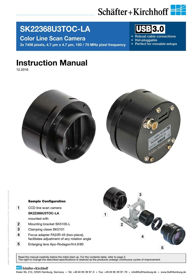
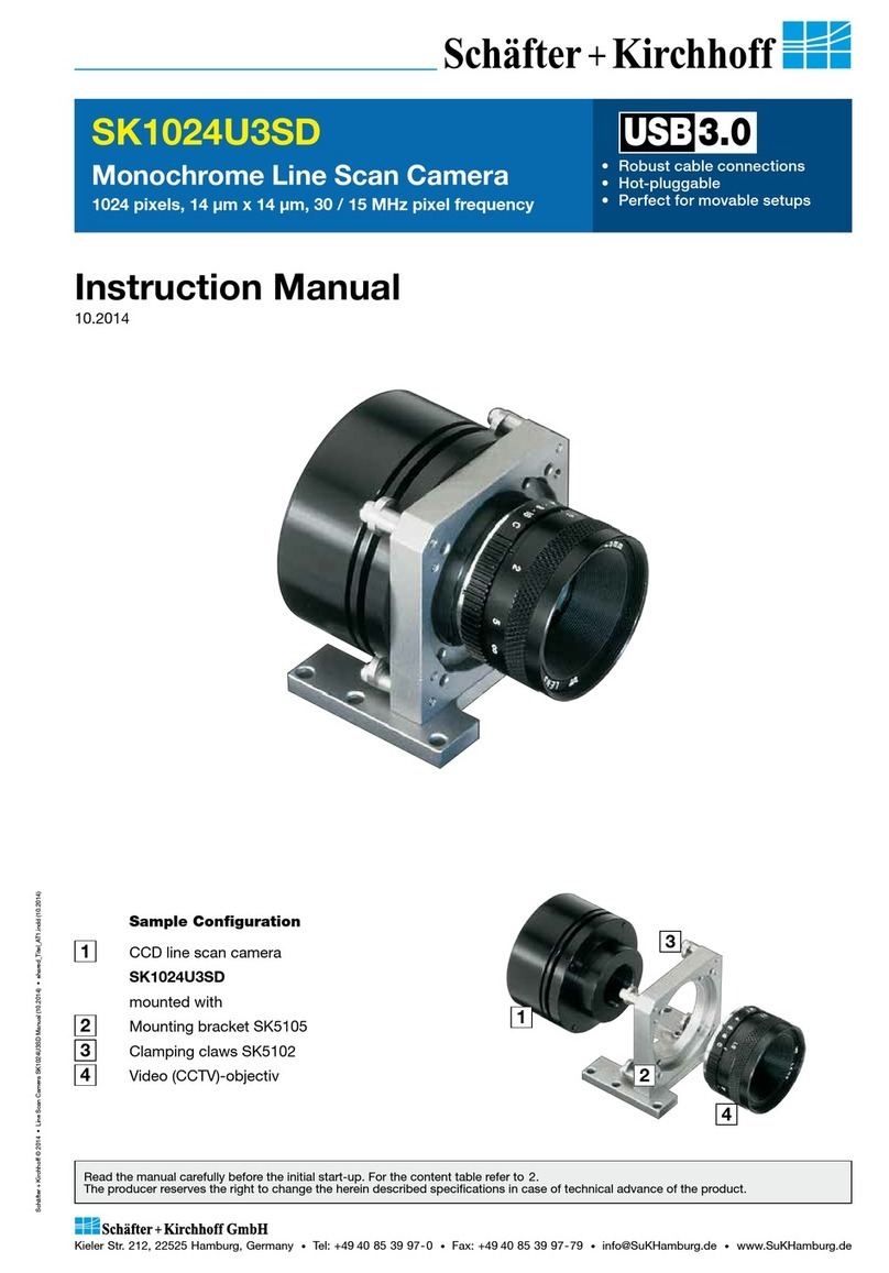
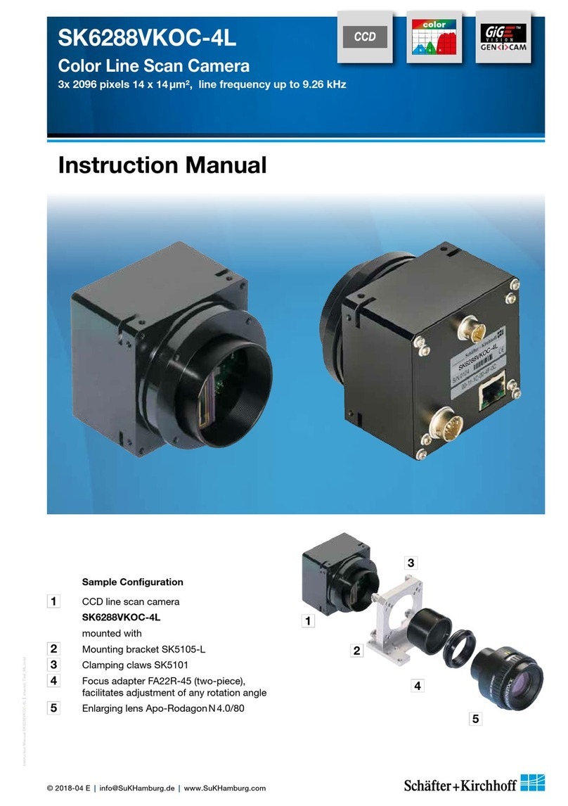
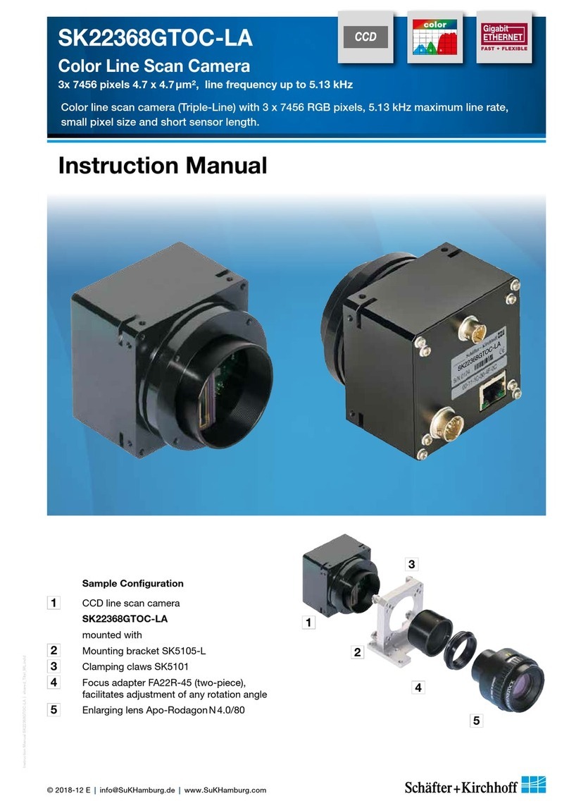
Schäfter+Kirchhoff SK 10680 DJR User manual

Performance Specifications
Accessories (optional)
Schäfter
+
Kirchhoff
SK_10680_DJR
Camera Type: SK 512 XSD
Order Code
Physical Characteristics
Sensor: CCD linear
Type ILX 550K
Pixel Number: 10680
Pixel Size: 4 µm x 4 µm
Pixel Distance: 4 µm
Line Distance: 4 µm
Active Length: 42,72 mm
Operating Ranges
Pixel Frequency: maximum 5 MHz
Line Frequency: maximum 0.465 kHz
minimum 0,05 kHz
Integration Time: minimum 2.15 ms
maximum 20 ms
Dynamic Range: 1 : 1000 (rms)
Spectral Range: 400-700 nm,
selectable (R,G or B)
www.SuKHamburg.de · eMail: info@SuKHamburg.de
Characteristic, Performance, Optional Accessories . . . . . . . . . . . . 1
1. Technical Specifications of the SK 10680DJR . . . . . . . . . . . . . . 2
2. Handling Details of the Line Scan Camera . . . . . . . . . . . . . . . . . 2
3. Connecting and Control Signals . . . . . . . . . . . . . . . . . . . . . . . . 3
Pin Assignment . . . . . . . . . . . . . . . . . . . . . . . . . . . . . . . . . . . . . 3
Voltage Supply . . . . . . . . . . . . . . . . . . . . . . . . . . . . . . . . . . . . . 3
4. Digital Control Signals . . . . . . . . . . . . . . . . . . . . . . . . . . . . . . . . .3
5. Exposure and Integration Control . . . . . . . . . . . . . . . . . . . . . . . 4
6. Generating an Image - Scan a Surface . . . . . . . . . . . . . . . . . . . .4
7. Timing Diagram . . . . . . . . . . . . . . . . . . . . . . . . . . . . . . . . . . . . . 5
8. Blooming . . . . . . . . . . . . . . . . . . . . . . . . . . . . . . . . . . . . . . . . . . 6
9. Gain / Offset - Settings . . . . . . . . . . . . . . . . . . . . . . . . . . . . . . . 7
10. References, Warranty and EC-Declaration of Conformity . . . . . 7
11. Dimension Diagrams . . . . . . . . . . . . . . . . . . . . . . . . . . . . . . . . 8
12. Sensor data . . . . . . . . . . . . . . . . . . . . . . . . . . . . . . . . . . . . . . . 9
Lenses Adapters
Characteristics
- high resolution Enlarging and
Macro Lenses
- high speed Photo Lenses
- Lenses including blocking brid-
ge for locking focal and aperture
setting.
Lens Adapter AOC-...
for adaptation of photo lenses
with bayonet mount
Focus Adapter FA22-...
for adaptation of enlangement
and macro lenses.
Camera Mount SK 5105
Order Code
Wrap resistant construction for mounting
the CCD Line Scan Camera.
Optional: Clamp set SK 5102 Order Code
to lock the CCD Line Scan Camera in
arbitrary rotation.
PC-Interface SK 9192 D
Order Code
Interface for digital CCD Line Scan Cameras
PCI-Bus, preprocessing on-board:
Shading Correction, Windowing, Thresholding
external synchronisation (Line- / Frame Sync)
Mounting Console SK5105-2
for the adaption of the macro
lens, extension rings ZR...,
focus adapter FA22-40 and
the CCD Line Scan Camera
Software SK91PCI-WIN *
SK91PCI-LX **
System software,
drivers, libraries
* Windows, ** Linux
Cable set SK9019 for digital
CCD Line Scan Cameras of the
series XSD, DPD, DPT, DJR, DJRC
etc.
36-filament shielded cable for camera control
and video signals. Standard: 3m cable length,
one- or two-sided Centronics connector (fe-
male).
• Digital camera 8 Bit resolution
• Triple line sensor
• Spectral range selectable (red,green,blue)
• Line frequency up to 0.46 kHz
• very light-sensitive
• LVDS interface
• low power consumption
• Round housing Ø 65 mm
SK 10680 DJR
Kieler Str. 212, D-22525 Hamburg - Tel: +49 (0)40 853997 0 - Fax: +49 (0)40 853997 79 - eMail: [email protected] - Web: http://www.SuKHamburg.de
SK9019.3 FF Order Code
FF =Connector two-sided (female)
F =Connector one-sided (female)
3 =3 m (standard cable length)
5 =5 m cable length
x =cable length coustom made
Typical Spectral Responsivity
Input Control SignalsMaster Clock
StartOfScan (SOS)
Output Signals
Video Signal: 8 Bit digital
Interface: LVDS
Power Supply
Voltage: +5 V, +15 V,
-15 V
Power Consumption:2 W
Connector
Mini Centronics 36 pin-male
Others:
Operating Temp.: + 5°C ... + 45 °
Size: Ø 65mm
x 51mm
Weight: 0.2 kg
Lens Thread: M 40 x 0.75
Content Page Page
24
1
CCD Line Scan Camera
SK 10680 DJR
mounting:
Camera mount SK5105
Clamp set SK5102
Photo lens with
blocking bridge
1
2
3
4
3
12
4
3
CCD LineScanCamera Digital b/w
SK 10680 DJR
10680 pixel, 4 x 4 µm, 5 MHz pixel frequency
Cable Connector:
Series Harting Bellows
Type: 6013 036 5100

Digital CCD Line Scan Camera SK 10680 DJR ( Rev.1.4. / 20.09.2005 ) - Manual Page 2
SK 10680 DJR
ILX 550K
10680
4 µm x 4 µm
4 µm
4 µm
42.72 mm
3)
no
no
no
5 MHz
2.15 ms
20 ms 2)
0.46 kHz
0.05 kHz
1 : 1000 (rms)
400 - 700 nm
8 Bit digital
LVDS
+5V, +15V, -15V
2W
M40 x 0.75
Ø65mm x 51mm
0.2 kg
+5°C ... +45°C
1. Technical Specifications of the DJR Series
Type of Camera
CCD Sensor
Number of pixels
Pixel Size
Pixel distance
Line distance
Active length
PRNU Photo Response
Non Uniformity
Anti-Blooming
Integration Control
CDS 1)
Max. pixel frequency
Min. integration time
Max integration time
Max. line frequency
Min. line frequency
Dynamic range
Spectral range
Video signal
Interface
Voltage supply
Power consumption
Lens connection
Housing
Weight
Temperatur range
1) CDS = Correlated Double Sampling. Noise reduction technology, increase of photosensitivity.
2) Longer exposure times are possible, but the signal-to-noise ratio will be reduced.
3) For further sensor specifications obtain the details of the sensor manufacturer. See the datasheet at the end.
2. Handling Details of the Line Scan Camera
Attention:
Bevore the Line Scan Camera is attached to or deta-
ched from the power supply make sure the power sup-
ply is switched off.
Otherwise, a permanent damage of the Line Scan
Camera is risked.
To prevent damage due to heat accumulation and keep
the temperature of the camera below 45°C, a sufficient air
circulation around the camera housing has to be ensured.
To start operation the camera has to be connected to
the necessary voltage, the MasterClock- and StartOfS-
can-Signals using a
36-pin Centronics Miniature
Connector.
The camera is shiped aligned and set to default settings
in gain and offset. Extensive modifications of the
gain/offset-parameter can lead to a decrease in signal
quality.
A successful application of the line scan camera is
based upon a careful adjustment of the whole optical
system. Attention should be paid to the arrangement of
the illumination, the aperture setting, the focussing
range of the lens, as well as the orientation of the sen-
sor axis to the scanning direction.
Recommendation:
Using the SK9192D PC-Interface and the SkLineScan®
software by Schäfter+Kirchhoff the camera is ready
for operation immediately. The oscilloscopical display of
the line scan camera signal including the zoom-function
and the online parameter setting of the camera is a
valuable tool while arranging the optical system setup.
The hardware preprocessing on the Interface board
(Shading Correction, Windowing, Thresholding) enables
recording and evaluation with maximum line frequency.
Furthermore, the comfortable methods of the class libraries
for C++ support the development of user software.

Digital CCD Line Scan Camera SK 10680 DJR ( Rev.1.4. / 20.09.2005 ) - Manual Page 3
3. Connecting and Control Signals
P1 P2
J1
Camera backside
J1 = Centronics 36pin-male, P1 = Offset adj., P2 = Gain adj.
Pin Assignment
Voltage Supply
+ 5 V ± 5% ca. 180 mA
+15 V ± 5% ca. 50 mA
-12V to -15 V ± 5% ca. 15 mA
4. Digital Control SIgnals
Input Control Signals:
The Low Voltage Differential input Signals (LVDS) are converted into TTL conform signals inside of the CCD camera.
The camera uses only the control signals "Clock" (MCLK) and "Start Of Scan" (SOS) for operation. The camera
electronic responds to the rising signal edges that should be ‘sharp’ and free from noise.
The frequency of the "Start of Scan" signal determines the total count of line scans per second. On the rising edge
of this signal all the accumulated charges inside the pixels will be tranferred to the analog shift register of the sensor.
The shift register (transport register) will be read out with the ‘Clock’ signal.
The ‘Clock’ signal frequency gives the read-out rate for single pixel informations of the linear sensor. This is just the
rate of the video output signal of the camera. Every rising edge of ‘Clock’ transfers the next following pixel’s char-
ges to the video output amplifier. Delay time at this point is about 50 ns.
The ‘Clock’ and the ‘SOS’ signals need not to be syncronized. The ‘Clock’ frequency should be set to a sufficient
large number to ensure enough ‘Clock’ pulses to read out the line sensor completely between two successive
‘SOS’ signals. The SK 10680 DJR Camera needs 10784 ‘Clock’ signals to read out a line scan completely. Gene-
rally, transferring a larger number of ‘Clock’ pulses as needed is unproblematic.
MCLK: Master-Clock in: determines the pixel transport frequency, maximum 5 MHz. Low voltage differential input.
SOS: Start of Scan: 50 ns minimum pulslength. Differential input.
The frequency of the ‘SOS’ signal determines the line frequency readout of the camera.
The charges of the sensor are accumulated while the ‘SOS’ signal is low. This way the length of the ‘low’
period can be used to effectively control the actual integration time at a fixed or rapidly changing line
frequency.
The rising edge of the ‘SOS’ signal initiates the readout operation and the charges are transferred into the
onchip analog shift register.
Output Signals:
‘Clock’ and ‘Start of Scan’ signals are echoed at the camera output to monitor system timings. These
signals, like the input ‘Clock’ and ‘Start of Scan’ signals, are ‘Low Voltage Differential signals’ (LVDS).
CCLK: Camera-Clock out / Low Voltage Differential driver.
LVAL: Line Valid / Differential driver. A ‘High’-level shows the availability of valid pixel data at the AD-converter out-
put. The signal ‘LVAL’ contains a ‘CLT’ pulse at the beginning of the line, necessary to synchronise
Schäfter+Kirchhoff - Interface boards.
D0-D7: 8 bit digital video output (8 x Low Voltage Differential driver LVDS) D0=LSB, D7=MSB
Miniature Centronics 36 pin Connector (male)
Signal Pin Pin Signal
GND 18 O O 36 GND
(+5V) VCC 17 O O 35 VCC (+5V)
GND 16 O O 34 D7 - out
(+5V) VCC 15 O O 33 D7 + out
CCLK - out 14 O O 32 D6 - out
CCLK + out 13 O O 31 D6 + out
LVAL - out 12 O O 30 D5 - out
LVAL + out 11 O O 29 D5 + out
SOS - in 10 O O 28 D4 - out
SOS + in 9 O O 27 D4 + out
MCLK - in 8 O O 26 D3 - out
MCLK + in 7 O O 25 D3 + out
GND 6 O O 24 D2 - out
(-12V bis -15V) VEE 5 O O 23 D2 + out
(+15V) VDD 4 O O 22 D1 - out
(+15V) VDD 3 O O 21 D1 + out
GND 2 O O 20 DO - out
Analog Video A out 1 O O 19 DO + out
(for test only)

Digital CCD Line Scan Camera SK 10680 DJR ( Rev.1.4. / 20.09.2005 ) - Manual Page 4
5. Exposure and Integration Control
Exposure:
The light sensitive elements of the sensor store the
charge which are generated by the incident light during
the exposure cycle. This accumulated charge is then
converted into voltage. These values are a measure for
the incident light intensity on each pixel.
The process of integration starts with the falling edge of
the ‘StartOfScan’ (SOS)-signal. While the SOS-signal is
‘Low’, charge is accumulated. With the rising edge of
the SOS-signal the exposure is concluded. The SOS-
signal level stays a short time on ‘High’, before the next
falling edge triggers the next exposure cycle.
Exposure time:
The exposure time of a single line scan tBis the time
interval of adjacent positive edges of the ‘StartOfScan’
(SOS)-signal. The time period of this interval (pixel
clock) is determined by the minimum number of
necessary pulses to read the accumulated charge into
the shift register of the line scan sensor.
The sum of the pixel clock pulses results from the
number of pixels N plus sensor dependent passive pixel
clock pulses NP. The camera SK10680DJR needs 104
pixel clock pulses. The read out frequency is
determined by the pixel frequency (MCLK). The
exposure time tBof a camera calculates:
( N + NP )
tB=fP
The line frequency is given by:
fL= 1/ tB
Integration Control (only SK 2048 DJRI - Camera):
In the default setting of the camera the SOS signal
between two exposure cycles shows ‘High’ only at very
few pixel clock pulses. The Integration time and the
exposure time are virtually of the same length.
The Integration Control function allows the extention of
the ‘High’-level condition in the SOS signal about a
specified number of pixel clock pulses. The start of the
accumulation of charge during an exposure cycle is
thus delayed.
The integration time tAis shortened to the difference of
during one exposure period necessary pixel clock
pulses ( N + NP ) and the specified number of clock
pulses for the extension of the ‘High’-level condition in
the SOS signal ( SOSL ).
The line scan frequency is not influenced by the
Integration Control function.
( N + NP ) - SOSL
tA=fP
•Exposure time: Time interval between successive
”SOS“ signals.
•Integration time: Duration of the actual charge
accumulation during the exposure time.
•Integration Control: for CCD line scan cameras it is
possible to program shorter integration times within
the actual exposure time (Shutter operation).
Beispiel: SK 10680 DJR, SK9192
5 MHz Pixelfrequenz
tB = (10680 + 136) / 5 MHz
tB = 2.15 ms
fL = 5 MHz / (10680 + 136)
fL = 0.46 kHz
Mode of operation of the Integration Control function
SOS
Accumulated
charge
This charge will be rejected This charge reaches the
shift register
6. Generating an Image – Scan a Surface
A two-dimensional image is generated by moving the
object or the camera. The direction of the movement
needs to be orthogonal to the sensor axis of the CCD
line scan camera.
To optain a propotional image with correct aspect ratios
a line synchronous transport and a laterally correct pixel
assignment is required.
WP•ββ
VO=tB
VO= Object rate
WP= Pixel width
ββ= Magnification
tB= Exposure time
Pixel 1
CCD Sensor
▲
Object
structure
▲

Digital CCD Line Scan Camera SK 10680 DJR ( Rev.1.4. / 20.09.2005 ) - Manual Page 5
7. Timing Diagram
* The rising edge of ‘SOS’ should not occur within a range of 5 to 30 ns before leading edge of ‘MCLK’.
** CLT = Camera Line Transfer ( internal line scan camera Signal)
*** The signal ‘LVAL’ contains a ‘CLT’ pulse at the line beginning, which is required for the synchronisation of
the Schäfter+Kirchhoff Interface boards.
If requested, the CCD line scan camera is available without ‘CLT’ pulse at the line beginning of the ‘LVAL’.
Order Code: SK 10680 DJR-3
The pixels determining the black level value are the 3th to the 51th before pixel no. 1.
i = Isolation pixels
o = Overclocking
MCLK
SOS *
CLT**
CCLK
LVAL***
Data
Video
internally
Input
Output
ca. 50 ns 97 Clock Cycles N= 10680 Clock Cycles 6 Clock Cycles min.
20 ns
00
10678 10679 10680
10680

Digital CCD Line Scan Camera SK 10680 DJR ( Rev.1.4. / 20.09.2005 ) - Manual Page 6
8. Blooming
Oscilloscopic display of line scan signals
(barcode illuminated with incident light),
SK 2048 DJRI
CCD line scan signal with increased illumination
in the center and sharp rising signal edges.
Zoomed detail from the center of the CCD line
scan signal in , integration time tA= 0.634 ms
Extended integration time tA= 2.419 ms. The sig-
nal edge is displaced slightly to the right. At an
overexposure of a factor of 3.8 the sensor starts
to bloom.
Overexposure caused by an increased integration
time results in signal deformations for sensors
without anti-blooming technology.
Charge by extreme overexposure penetrate the
following scan and cause an overload of the black
level pixel values. The offset control unit of the
camera is disturbed and the CCD line scan
camera supplies a reduced signal.
1
1
Blooming
Extended illumination of saturated pixels, which are
not able to accumulate further charge due to long
exposure, leads to charge overflow into adjacent
pixels. This effect is called blooming. Blooming
causes a corruption of the geometrical allocation of
image and object in the line signal.
CCD line scan cameras with anti-blooming sensors
direct the abundant charge to a ”drain gate”. Charge
overflow into adjacent, less illuminated pixels is
prevented. Depending on pixel frequency and
spectral range, overexposure up to factor of 50 can
thus be handled.
The CCD line scan cameras of the SK 10680DJR do not
contain anti-bloooming sensors. Nevertheless, they are
prevented from overexposure due to a special design.
DJR-cameras can be densed to a factor of 3.8, without
blooming the sensor.
Figure shows the line scan signal of a SK2048DJRI-
camera with increased illumination in the center. For a
better visualisation of the blooming effect the saturation
voltage of the sensor VSAT was reduced to roughly 90%
of the maximum ADC-voltage. Thus, even with overex-
posure the maximum of 255 of the 8-bit digitized signal
intensity will not be reached. In the central section the
sensor is on the verge of saturation.
The marked region from figure is zoomed in figure .
Here, the integration time tAamounts to 0.634 ms.
In figure the integration time was increased to tA
2.419 ms. Only from this point on the sensor starts to
bloom. The signal edge is displaced slightly to the right,
caused by excessive charge congesting the adjacent
pixels.
Even longer integration times result in an intolerable
deformations of the signal structures. In figure the
integration time was set to tA3.38 ms, corresponding in
an overexposure of a factor of 5.3.
Figure shows a phenomenon at extreme overexpo-
sure of CCD line scan cameras. The large charge
excess of the preceding scan leads in the shown sam-
ple to an overload of the pixels at the beginning of the
line. In this area the pixels determining the dark level are
located. These pixels are used as a reference for the off-
set control. The large dark level intensity induces a
reduction of the total signal intensity. Under these con-
ditions more light generates a smaller signal intensity at
the camera output.
In case of a very small output signal at operation start
up of the CCD line scan camera, an extreme overexpo-
sure can be the reason.
Consider:
CCD line scan cameras including anti-blooming sen-
sors can be densed to a factor of 50 before showing any
effect of blooming.
5
4
3
21
1
2
5
3
4
1
2
3
4
5
einsetzendes Blooming
dark level values raised by roaming change of preceding scan

Digital CCD Line Scan Camera SK 10680 DJR ( Rev.1.4. / 20.09.2005 ) - Manual Page 7
9. Gain / Offset - Settings
P1 P2
Camera backside
To adjust the gain / offset settings the camera does
not need to be opened. The trimmers for balancing
P1 and P2 are accessible from the outside.
The camera is shiped with optimum Gain / Offset
calibration. If a recalibration becomes necessary
please follow the instructions given below:
1. Adjust the individual offset of the line sensor video
signal to zero voltage (‘00’ digital) using P1.
2. Use P2 to adjust the maximum output voltage.
Illuminate the camera sufficiently.
The maximum output voltage is set to ca. 2.5 volts
standard (‘FF’ digital).
Camera board,
sensor side
The spectral range of the camera can be select by
soldering a bridge over the appropriate pads.
B
R
G
Although this manual has been reviewed carefully for
technical accuracy, errors are possible. The reader is
kindly asked to contact us, if errors are suspected.
The indicated circuits, descriptions and tables are not
warranted to be free from rights of third parties.
With the statements in the technical descriptions only
assembly groups are specified. Characteristics as well
as the suitability for a particular purpose is not guaran-
teed.
The warranty period for the CCD line scan camera is 24
months. The warranty ends with inappropriate actions.
10. References and Warranty
EC-Declaration of Conformity
This product meets the requirement
of the EC directive 89/336/E.E.G.
The requirements of DIN EN 61326
are fullfilled.

Digital CCD Line Scan Camera SK 10680 DJR ( Rev.1.4. / 20.09.2005 ) - Manual Page 8
11. Dimension Drawings
Camera mount
SK 5105
for digital and analog cameras
Order Code: SK 5105
Wrap resistant construction for
mounting a CCD Line Scan Camera
Clamp set SK 5102
(4 units)
to lock the CCD Line Scan Camera in
arbitrary rotation.
CCD line scan cam. digital
Lens thread M40 x 0.75
mounted on:
Camera mount SK 5105
Clamp set SK 5102
for locking the CCD Line Scan
Camera in arbitrary rotation
66 50
2016.5
3.5 6.5
1010
36
M3
M3 Ø3.3
Ø4.3
6
15
50.3
41.7
70
63
40
M4
1/4’’ 20G
Clamp
Cylinder screw
DIN 912–M3x12
CCD line scan camera digital
Lens thread: M40 x 0.75
distance to sensor: 19.5 mm
Connector: Centronics miniature
36 pin-male
Type of Cameras:
SK 10680 DJR
1
2
3
4
CCD line scan camera
digital
Lens thread M40 x 0.75
mounted on:
Camera mount SK 5105
Clamp set SK 5102
Cable set SK 9019.3.FF
Lens
Blockingbridge(apertureandfocus)
1
123 5
2
3
4
5
Lens, e. g.: Photo lens MD by Minolta
Lens thread: M40 x 0.75
1:1.7, f’ = 50 mm, sensor length max. 35 mm
5
65 min.
*
*
4
Further video, enlargement and
macro lenses: siehe Prospekt
CCDLineScanCameras 2002E p. K9
68,5
optional
Locking using 4 units
cylinder screws
DIN 912 - M3x16
6
6
1
2
3
4
5
1
5
2
*
Ø42

Digital CCD Line Scan Camera SK 10680 DJR ( Rev.1.4. / 20.09.2005 ) - Manual Page 9
12. Sensor Data
Manufacturer: SONY®
Type: ILX 550K
Data: SONY® - CCD Linear Sensor - DataSheet
Block Diagram

Digital CCD Line Scan Camera SK 10680 DJR ( Rev.1.4. / 20.09.2005 ) - Manual Page 10

Digital CCD Line Scan Camera SK 10680 DJR ( Rev.1.4. / 20.09.2005 ) - Manual Page 11
Table of contents
Other Schäfter+Kirchhoff Security Camera manuals

Schäfter+Kirchhoff
Schäfter+Kirchhoff SK12240U3KOC-LB User manual

Schäfter+Kirchhoff
Schäfter+Kirchhoff SK1024VSD User manual

Schäfter+Kirchhoff
Schäfter+Kirchhoff SK8100U3JRC User manual

Schäfter+Kirchhoff
Schäfter+Kirchhoff SK6288VKOC-4L User manual

Schäfter+Kirchhoff
Schäfter+Kirchhoff SK22368U3TOC-LA User manual

Schäfter+Kirchhoff
Schäfter+Kirchhoff SK22368GTOC-LA User manual

Schäfter+Kirchhoff
Schäfter+Kirchhoff SK1024U3SD User manual

Schäfter+Kirchhoff
Schäfter+Kirchhoff SK1024U3HU User manual

Schäfter+Kirchhoff
Schäfter+Kirchhoff SK512CSH User manual

Schäfter+Kirchhoff
Schäfter+Kirchhoff SK22368U3TOC User manual