GS3471
Evaluation Board User Guide Rev.3
PDS-061243 March 2018
2 of 22
Semtech
Proprietary & Confidential
www.semtech.com
Revision History
Contents
1. EB-GS3471-00 User Guide ............................................................................................................................5
1.1 Power (J5 or J13) .................................................................................................................................5
1.2 SDI Input (J6 and J7) ..........................................................................................................................6
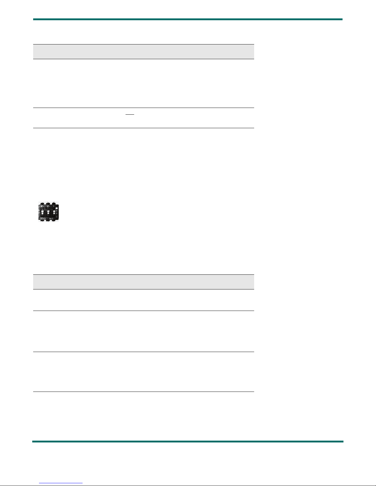
1.3 Switch Settings (SW1 and SW2) ....................................................................................................6
1.3.1 GS3471 Switch Settings (SW1)...........................................................................................6
1.3.2 GS2988 Switch Settings (SW2)...........................................................................................7
1.4 3G-SDI Loop Through (J10) .............................................................................................................8
1.5 Video Header (J1) ...............................................................................................................................8
1.6 Audio Header (H1, J4 and J12) .......................................................................................................9
1.6.1 Audio Header (H1) .................................................................................................................9
1.6.2 AES Model — RCA Connectors (J4 and J12) .............................................................. 10
1.7 JTAG Header ...................................................................................................................................... 11
1.8 Status LED’s ....................................................................................................................................... 11
1.9 Modes of Operation ........................................................................................................................ 12
2. EB-GS3471-00 Schematics......................................................................................................................... 13
3. EB-GS3471-00 Board Layout..................................................................................................................... 17
4. EB-GS3471-00 Bill of Materials (BOM).................................................................................................... 19
Version ECO PCN Date Changes and/or Modifications
3 041088 — March 2018 Updated Section 1.1.
2 038786 — September 2017
Digital and analog ground pin names updated to CORE_GND
and A_GND respectively.
Updates to Pin A1, A2, F1, G1 in Figure 2-3.
1 034214 — November 2016 Pin A7 changed to RSVD in Figure 2-3.
0 030575 — May 2016 New document.