XE-A40S
1 – 2
The mode switch has these settings:
[5] DISPLAY
1. OPERATOR DISPLAY
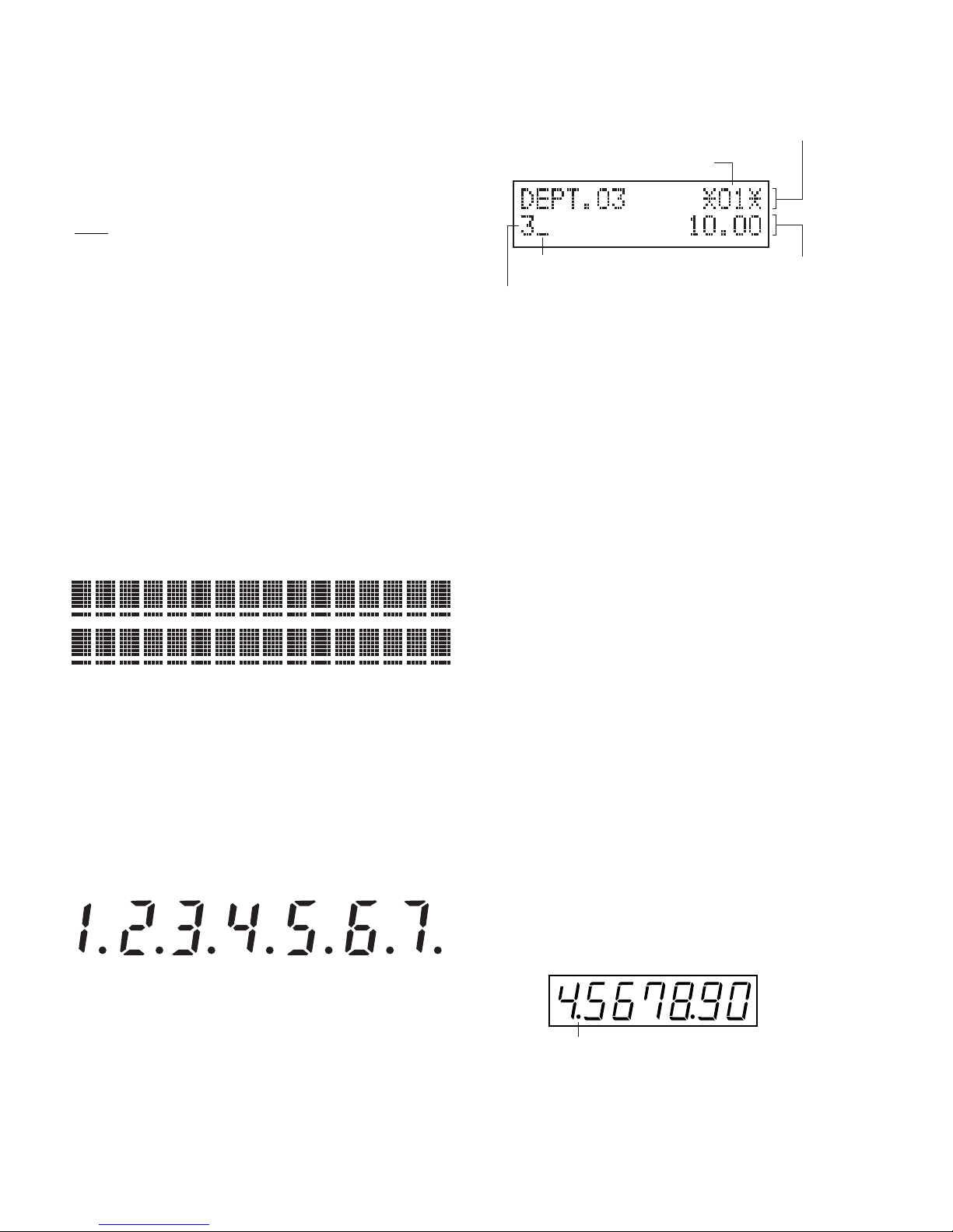
Layout:
2. CUSTOMER DISPLAY
Layout:
3. DESCRIPTION
3.1. Operator display
• Clerk code or Mode name
The mode you are in is displayed. When a clerk is assigned, the
clerk code is displayed in the REG or OP X/Z mode. For example,
"*01*" is displayed when clerk 01 is assigned.
• Repeat
The number of repeats is displayed, starting at "2" and incremental
with each repeat. When you have registered ten times, the display
will show "0" (2→3......9→0→1→2...)
• Sentinel mark
When amount in the drawer reaches the amount you prepro-
grammed, the sentinel mark "X" is displayed to advise you to
remove the money and put it in a safe place.
• Power save mark
When the cash register goes into the power save mode, the power
save mark (decimal point) lights up.
• Function message display area
Item labels of departments and PLU/subdepartments and function
texts you use, such as %1, (-) and CASH are displayed.
When an amount is to be entered or entered, "AMOUNT" is dis-
played: When an amount is to be entered, ------- is displayed at the
numeric entry area with "AMOUNT". When a preset price has been
set, the price is displayed at the numeric entry area with
"AMOUNT".
• Numeric entry display area
Numbers entered using numeric keys are displayed here.
*Date and time display
Date and time appear on the display in the OP X/Z, REG, or MGR
mode. In the REG or MGR mode, press the [#/TM/SBTL] key to
display the date and time.
*Error message
When an error occurs, the corresponding error message is dis-
played in the function message display area.
3.2. Customer display (Pop-up type)
OFF: This mode locks all register operations. (AC power turns
off.)
No change occurs to register data.
OP X/Z: To take individual clerk X or Z reports, and to take flash
reports.
It can be used to toggle receipt state "ON" and "OFF" by
pressing he [RCP/PO] key.
REG: For entering sales.
PGM: To program various items.
VOID: Enters into the void mode. This mode allows correction
after finalizing a transaction.
MGR: For manager's entries. The manager can use this mode
for an override entry.
X1/Z1: To take the X/Z report for various daily totals.
X2/Z2: To take the X/Z report for periodic (weekly or monthly)
consolidation.
Display device : LCD
Number of line : 2 line
Number of positions : 16 positions
Color of display : Yellow / Green
Character form : 7 segment + Dp
Character size : Approx. 8.0mm (H) x 4.8mm (W)
Display device : LED
Number of line : 1 line
Number of positions : 7 positions
Color of display : Yellow / Green
Style : Pop up type
Character form : 7 segment + Dp
Character size : 14.0mm (H) x 8.0mm (W)
Function message display area
Clerk code or mode name
Numeric entry display area
Receipt OFF indicator
Repeat / Sentinel mark / Power save mark
Power save mark
(Lighting the mark only under the power save mode)