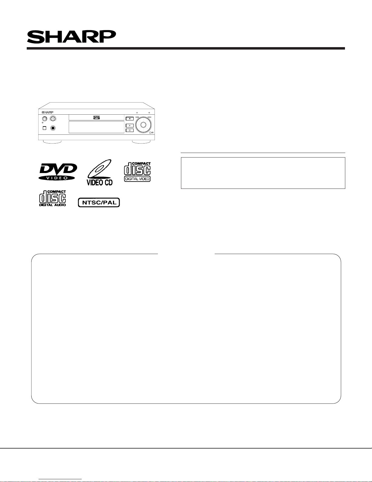
DV-600S
DV-600H
8-3. POLARITIES OF SIGNAL
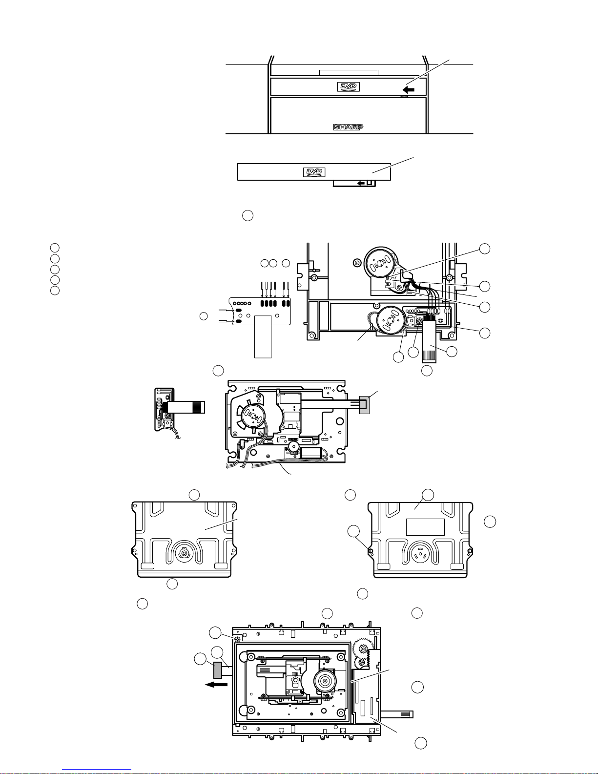
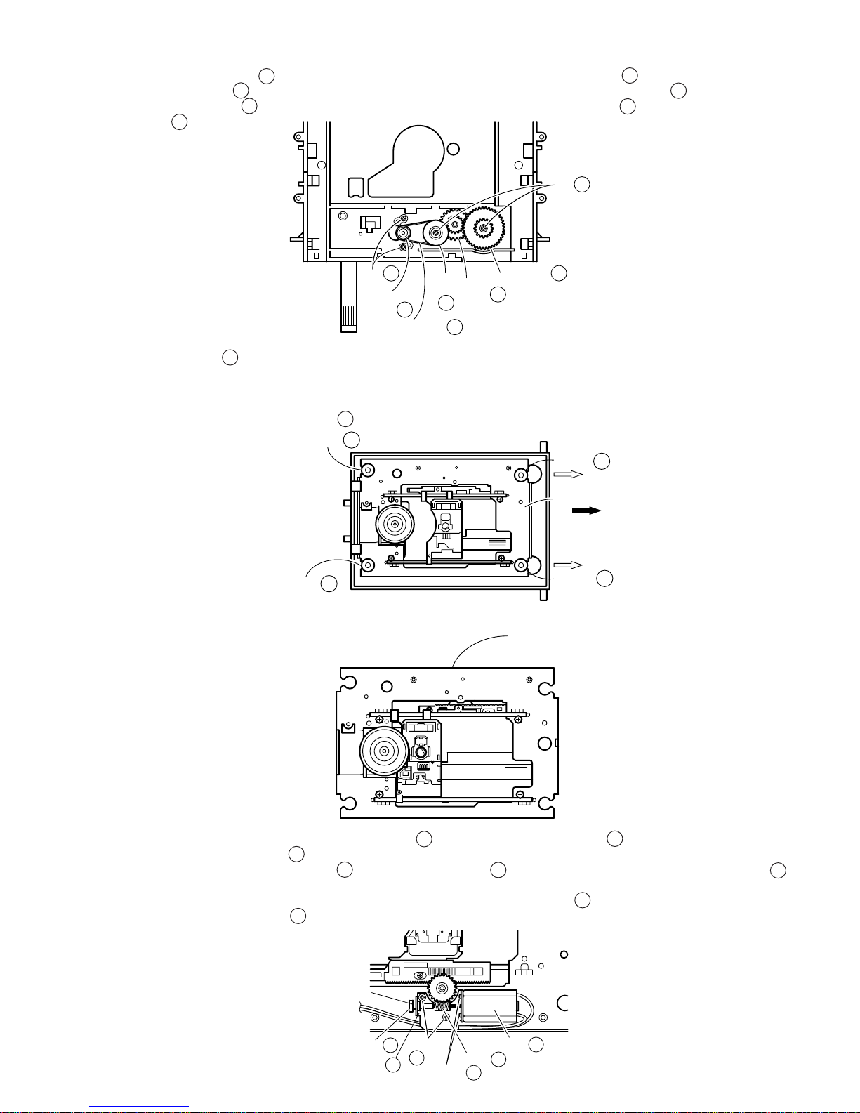
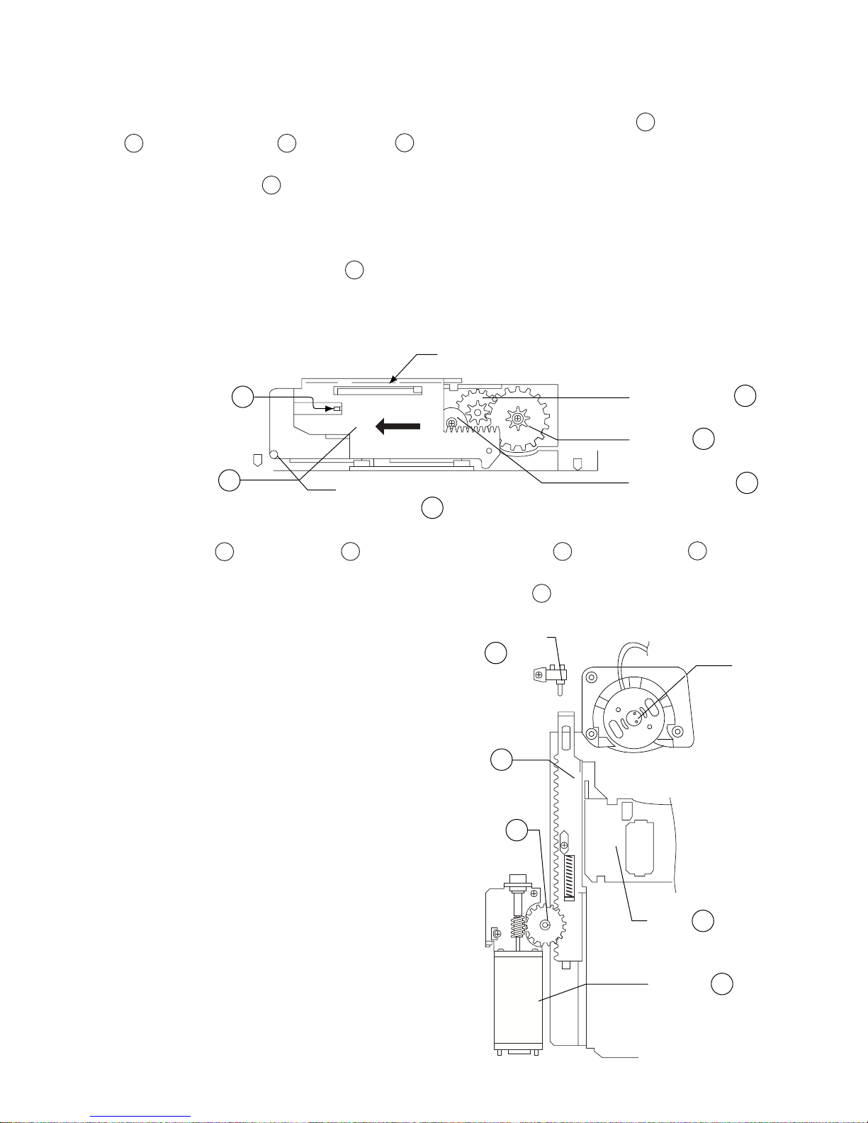
8. OPERATION OF PICKUP
8-1. CIRCUIT CONFIGURATION OF PICKUP
The pickup unit reads signals from the disk, and the flexible cable is connected to the board. The following signals flow through the
cable.
8-2. EQUIVALENT CIRCUIT OF PICKUP
FO+
TR–
TR+
FO–
ACTUATOR
OSC VOS
LD
PD
VA
VB
VC
VD
Sga
Vraf
Vcc
GND
–
+
–
+
–
+
–
+
HOLOGRAM LASER UNIT
1
2
3
4
5
6
7
8
9
10
11
12
13
14
15
16
17
18
19
20 1
TR–
FO+
TR+
FO–
VR
PD
VCC
GND
LD
GND
VOS
NC
NC
Vref(VCC/2)
VA
VC
Sga
GND
VB
VD
(NC)
Power adjust
HIGH-FREQUENCY CONVOLUTION
Focus When electric current is flowed
FO+, FO- from FO+ to FO-, the lens comes
to near the disk.
Tracking When electric current is flowed
TR+, TR- from TR+ to TR-, the lens goes
toward the outer circumference.
Gain switching DVD one Layer High gain
Sga DVD two Layer Sga : +5V
CD
8-4. SIGNALS OF PICKUP
8-4-1. Tracking drive signal (TR+, TR-)
The signal drives the tracking servo mechanism which projects the beam on the track by moving the objective lens (OL) to the outer
or inner circumference (at a right angle against the track) of the disk.
2-focus objective lens
Actuator assembly
Monitor Diode
Basic Structure of Laser Diode
Laser Diode
LD PD
8-1
8-4-2. Focus drive signal (FO+, FO-)
The signal drives the focus servo mechanism which aligns the focus on the pit of the disk
by elevating OL (vertically against the disk surface.)
The VR terminal is connected to GND.
8-4-3. Monitor Diode (PD)
Since the laser diode largely varies output of the laser light even if the flowing current is slightly varied, the projection
light is detected with the monitor diode to control the laser light to be equally output.
Since the current varies on the monitor diode according to the intensity of the received light of the laser diode, the drive current of
thelaserdiodeisreducedifthecurrentofthemonitordiodeincreases.Onthecontrary,thedrivecurrentofthelaserdiodeisincreased
if the current of the monitor diode decreases.
As the projection light of the laser diode becomes stronger, the current of the monitor diode increases to increase the current which
flows into the monitor diode output (PD). This is input to the pin 44 of IC303 and is compared with the reference voltage to control
the drive current of the laser diode.
The circuit is called ALPC (Automatic Laser Power Control).
8-4-4. Laser diode drive current control (LD)
Power supply to drive the laser diode
8-4-5. High-frequency convolution module power supply (VOSC)
The high-frequency convolution imposes the high-frequency signal on the DC current to impose the high frequency on the drive
current of the laser. Thus, the interference of outgoing light and reflected light is prevented.
8-4-6. HF Signal (VA, VB, VC, VD)
Signals recorded in the disk When the quantity of laser light increases, the current shown in
figure increases and the PD terminal voltage rises.
IC303 is used to control. The LD terminal voltage lowers, and
the quantity of light reduces. (IC303 is actuated by voltage
input.)
 User manual")


 User manual")


 User manual")


 User manual")


 User manual")


 Guide")


 User manual")