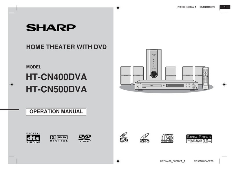
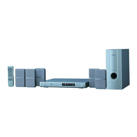
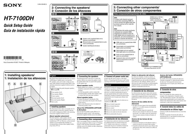
Sharp HT-CN300 User manual

HT-CN300
No. S7250HTCN300/
CONTENTS
Page
IMPORTANT SERVICE NOTES (FOR U.S.A. ONLY)....................................................................................................... 2
SPECIFICATIONS ............................................................................................................................................................. 3
NAMES OF PARTS ........................................................................................................................................................... 4
DISASSEMBLY.................................................................................................................................................................. 6
ADJUSTMENT ................................................................................................................................................................... 8
NOTES ON SCHEMATIC DIAGRAM ................................................................................................................................ 9
TYPES OF TRANSISTOR AND LED................................................................................................................................. 9
BLOCK DIAGRAM ........................................................................................................................................................... 10
SCHEMATIC DIAGRAM .................................................................................................................................................. 14
VOLTAGE ........................................................................................................................................................................ 31
WIRING SIDE OF P.W.BOARD....................................................................................................................................... 32
FUNCTION TABLE OF IC................................................................................................................................................ 38
FL DISPLAY..................................................................................................................................................................... 44
REPLACEMENT PARTS LIST/EXPLODED VIEW
PACKING OF THE SET (FOR U.S.A. ONLY)
SERVICE MANUAL
This document has been published to be used
for after sales service only.
The contents are subject to change without notice.
SHARP CORPORATION
• In the interests of user-safety the set should be restored to its
original condition and only parts identical to those specified be
used.
HOME CINEMA COMMAND
MODEL HT-CN300(BK)
HT-CN300 Home Cinema Command consisting of HT-CN300 (main unit),
CP-CN300F(frontspeakers),CP-CN300C(centerspeaker)andCP-CN300R
(surround speakers).
HOME CINEMA COMMAND
MODEL HT-CN300(S)
HT-CN300HomeCinemaCommandconsistingofHT-CN300(main
unit), CP-CN300F (front speakers), CP-CN300C (center speaker)
and CP-CN300R (surround speakers).

HT-CN300
– 2 –
IMPORTANT SERVICE NOTES (FOR U.S.A. ONLY)
BEFORE RETURNING THE AUDIO PRODUCT
(Fire & Shock Hazard)
Before returning the audio product to the user, perform the
following safety checks.
1. Inspect all lead dress to make certain that leads are not
pinchedorthathardwareisnotlodgedbetweenthechassis
and other metal parts in the audio product.
2. Inspect all protective devices such as insulating materials,
cabinet,terminalboard,adjustmentandcompartmentcovers
or shields, mechanical insulators etc.
3. To be sure that no shock hazard exists, check for leakage
current in the following manner.
* Plug the AC line cord directly into a 120 volt AC outlet.
* Using two clip leads, connect a 1.5 kohm, 10 watt resistor
paralleled by a 0.15 µF capacitor in series with all exposed
metal cabinet parts and a known earth ground, such as
conduit or electrical ground connected to earth ground.
* Use a VTVM or VOM with 1000 ohm per volt, or higher,
sensitivity to measure the AC voltage drop across the
resistor (See diagram).
* Connect the resistor connection to all exposed metal parts
havingareturnpathtothechassis(antenna,metalcabinet,
screw heads, knobs and control shafts, escutcheon, etc.)
and measure the AC voltage drop across the resistor.
AllcheckmustberepeatedwiththeAClinecordplugconnection
reversed.
Anyreading of0.3 voltRMS (thiscorresponds to0.2 milliamp.
AC.) or more is excessive and indicates a potential shock
hazard which must be corrected before returning the audio
product to the owner.
TO EXPOSED
METAL PARTS
CONNECT TO
KNOWN EARTH
GROUND
TEST PROBE
0.15 µF
1.5 kohms
10 W
VTVM
AC SCALE

– 3 –
HT-CN300
General
Amplifier
Tuner
Power source AC 120 V, 60 Hz
Power consumption 195 W
Dimensions Width: 9-1/8" (230 mm)
Height: 14-7/8" (377 mm)
Depth: 15-3/4" (400 mm)
Weight 24.3 lbs. (11.0 kg)
Terminals Front speakers, Center speaker and Surround speakers:
6 ohms
Monitor output: S-video/video
Video output (Video 1): RCA type
Audio output (Video 1): RCA type (L/R)
Video input (Video 1): RCA type
Audio input (Video 1): RCA type (L/R)
Audio input (Auxiliary): RCA type (L/R)
Video input (Video 2): RCA type
S-video input (DVD): S-terminal
Video input (DVD): RCA type
Audio input (Video 2): RCA type (L/R)
Digital input (DVD): Optical
Digital input (DVD): Coaxial
Power output (FTC) 30 watts minimum RMS per channel into 6 ohms from 200
Hz to 20 kHz, 10 % total harmonic distortion
Rated power output Front: 30 W + 30 W (10% T.H.D, 1 kHz)
Center: 30 W (10% T.H.D, 1 kHz)
Surround: 30 W + 30 W (10% T.H.D, 1 kHz)
Subwoofer: 30 W (10% T.H.D, 100 Hz)
Frequency range FM: 87.5 - 108 MHz
AM: 530 - 1,720 kHz
Type Full Range Speaker System (Magnetic shield)
3-1/8" (80 mm) speaker
Maximum input power 60 W
Rated input power 30 W
Impedance 6 ohms
Dimensions Width: 4-1/8" (104 mm)
Height: 4-3/8" (110 mm)
Depth: 4-7/8" (123 mm)
Weight 1.8 lbs. (0.8 kg)/each
Type Subwoofer System (Magnetic shield)
6-1/4" (160 mm) Woofer
Maximum input power 60 W
Rated input power 30 W
Impedance 6 ohms
SPECIFICATIONS
HT-CN300 (Except for Canada)
CP-CN300F/CP-CN300C/CP-CN300R (Except for Canada)
Specifications for this model are subject to change without
prior notice.
Subwoofer (Except for Canada)
FOR A COMPLETE DESCRIPTION OF THE OPERATION OF THIS UNIT, PLEASE REFER
TO THE OPERATION MANUAL.
HT-CN300 (For Canada)
General
Amplifier
Tuner
Power source AC 120 V, 60 Hz
Power consumption 195 W
Dimensions Width: 230 mm (9-1/8")
Height: 377 mm (14-7/8")
Depth: 400 mm (15-3/4")
Weight 11.0 kg (24.3 lbs.)
Terminals Front speakers, Centre speaker and Surround speakers:
6 ohms
Monitor output: S-video/video
Video output (Video 1): RCA type
Audio output (Video 1): RCA type (L/R)
Video input (Video 1): RCA type
Audio input (Video 1): RCA type (L/R)
Audio input (Auxiliary): RCA type (L/R)
Video input (Video 2): RCA type
S-video input (DVD): S-terminal
Video input (DVD): RCA type
Audio input (Video 2): RCA type (L/R)
Digital input (DVD): Optical
Digital input (DVD): Coaxial
Rated power output Front speakers:
RMS: 60 W (30 W + 30 W) (10 % T.H.D., 1 kHz)
Centre speaker:
RMS: 30 W (10 % T.H.D., 1 kHz)
Surround speakers:
RMS: 60 W (30 W + 30 W) (10 % T.H.D., 1 kHz)
Subwoofer:
RMS: 30 W (10 % T.H.D., 100 Hz)
Frequency range FM: 87.5 - 108 MHz
AM: 530 - 1,720 kHz
Type Full Range Speaker System (Magnetic shield)
80 mm (3-1/8") Speaker
Maximum input power 60 W
Rated input power 30 W
Impedance 6 ohms
Dimensions Width: 104 mm (4-1/8")
Height: 110 mm (4-3/8")
Depth: 123 mm (4-7/8")
Weight 0.8 kg (1.8 lbs.)/each
Type Subwoofer System (Magnetic shield)
160 mm (6-1/4") Woofer
Maximum input power 60 W
Rated input power 30 W
Impedance 6 ohms
CP-CN300F/CP-CN300C/CP-CN300R (For Canada)
Subwoofer (For Canada)
HT-CN300
– 4 –
NAMES OF PARTS
HT-CN300
Remote control
1. Power Button
2. Operation Buttons for Other Equipment
3. Remote Control Transmitter
4. Sound Mode Select Buttons
5. Dynamic Sound Select Button
6. Remote Control Sensor for Learn Function
7. Speaker Set Up Button
8. Clear Button
9. Learn Indicators
10. Volume Up and Down Buttons
11. DVD Button
12. Video-1 Button
13. Tuner/Band Button
14. Video-2/Auxiliary Button
15. Memory 1/2 Buttons for Other Equipment
16. Label Sealing Area
17. Clock Button
18. Memory Button
19. Timer/Sleep Button
20. Display Button
21. Dimmer Button
22. Extra Bass/Demo Mode Button
23. Equalizer Mode Selector Button
24. Cursor Button
25. Enter Button
26. Learn/Transmit Selector Switch
27. 3.6 V DC Input Jack
28. Memory 1/2 Selector Switch
256
34 78 9
17
18
19
20
21
22
23
15
16
15
16
14
13
12
11
10
24 25
26
27
28
1
Main unit (with subwoofer)
1. Memory Indicator
2. Timer Play Indicator
3. Sleep Indicator
4. Extra Bass Indicator
5. Digital Theater System Indicator
6. FM Stereo Mode Indicator
7. FM Stereo Receiving Indicator
8. Dolby Pro Logic II Indicator
9. Dolby Virtual Indicator
10. Dolby Digital Indicator
11. Power Indicator
12. Power Button
13. Remote Control Sensor Jack
14. TV Monitor Output Jacks
15. DVD Video Input Jacks
16. Video and Audio Input Jacks (VIDEO 2)
17. Video and Audio Input Jacks (VIDEO 1)
18. Subwoofer
19. AC Power Cord
20. DVD Optical Digital Audio Input Jack
21. DVD Coaxial Digital Audio Input Jack
22. FM/AM Loop Antenna Jack
23. Video and Audio Output Jacks (VIDEO 1)
24. Auxiliary Audio Input Jacks
25. Speaker Terminals
14
21
22
23
24
25
15
16
17
18
19
20
12
13
12 345
8
67
9
10
11
Front
Back

– 5 –
HT-CN300
1. Full-Range Speaker
2. Angle Adjusting Lever
3. Label indication
4. Mounting Slot
5. Speaker Terminals
6. Mounting Screw Holes
Remote control sensor
1. Remote Sensor
2. Remote Control Indicator
3. Remote Sensor Connection Plug
Caution:
Carefully choose where you place the remote control sensor as the tape adhesive
may damage or peel the surface coating when the tape is removed.
Never locate the remote control sensor in an unstable place. Otherwise it may fall.
Note:
Fix the remote control sensor on a flat surface.
1
1
3
2
2
5
Bottom
Front Side
6
4
3
Front Speaker (right): Red
Front Speaker (left): White
Center Speaker: Green
Surround Speaker (right): Gray
Surround Speaker (left): Blue
Speaker cushion:
Attach the cushions to the bottom of the speakers to prevent
them from sliding.
Double-sided tape for remote control sensor:
You can fix the remote control sensor with the supplied tape.
HT-CN300
CP-CN300F/CP-CN300C/CP-CN300R

HT-CN300
– 6 –
Top Cover A LCD Cover
Top Cover B
Back Cover R Back Cover L
(A1)x2
ø3x8mm
(B1)x2
ø2.5x12mm
(D1)x6
ø3x8mm
1 Top Cover B 1. Screw ...................... (A1) x2 6-1
2 LCD Cover 1. Hexagon Screw ...... (B1) x2 6-1
3 Top Cover A/ 1. Screw ...................... (C1) x4 6-2
LCD PWB 2. Flat Cable ............... (C2) x3
3. Screw ...................... (C3) x4
4 Back Cover L/R/ 1. Screw .................... (D1) x25 6-1, 7-1
Rear Panel
5 DSP PWB 1. Screw ...................... (E1) x2 7-2
2. Socket ..................... (E2) x1
3. Flat Cable ............... (E3) x4
4. PWB Holder ............ (E4) x2
6 Subwoofer Stand/ 1. Screw .......................(F1) x4 7-2
PWB Unit 2. Screw .......................(F2) x2
3. Socket ......................(F3) x1
7 Video PWB 1. Screw ...................... (G1) x3 7-3
2. Socket ..................... (G2) x2
8 Audio PWB 1. Screw...................... (H1) x2 7-3
9
AMP. PWB
1. Screw ....................... (J1) x6 7-3
2. Socket ...................... (J2) x4
10 Speaker PWB 1. Screw ...................... (K1) x1 7-3
11 Subwoofer 1. Screw .......................(L1) x4 7-2
DISASSEMBLY
Figure 6-2
STEP REMOVAL PROCEDURE FIGURE
Figure 6-1
HT-CN300
HT-CN300
DSP PWB
LCD PWB
Top Cover A
(C3)x4
ø3x8mm
(C1)x2
ø4x12mm
(C1)x2
ø4x20mm
(C2)x3
Caution on Disassembly
Follow the below-mentioned notes when disassembling
the unit and reassembling it, to keep it safe and ensure
excellent performance:
1. Be sure to remove the power supply plug from the wall
outlet before starting to disassemble the unit.
2.Takeoffnylon bands orwireholderswherethey need to
beremovedwhendisassemblingtheunit.Afterservicing
theunit,besure to rearrange theleadswheretheywere
before disassembling.
3. Take sufficient care on static electricity of integrated
circuits and other circuits when servicing.

– 7 –
HT-CN300
Figure 7-2
Figure 7-3
Figure 7-1
DSP PWB
Rear Panel
Subwoofer Box
(D1)x19
ø3x8mm
DSP PWB
DSP PWB
Push
Pull
(E3)x2
PWB
Unit
(E3)x2
(E4)x2
(E2)x1
(E1)x2
ø3x8mm
1 Push1
2
(F2)x2
ø4x16mm
(L1)x4
ø4x12mm
Subwoofer Stand
Subwoofer
(F1)x3
ø4x20mm
(F1)x1
ø4x20mm
(F3)x1
(G1)x3
ø3x8mm
(G2)x1
(G2)x1
(J2)x2
(H1)x2
ø3x8mm
(K1)x1
ø3x8mm
(J1)x6
ø3x8mm
(J2)x1
Tuner
PWB
Tuner PWB
(J2)x1
AMP.
PWB AMP.
PWB
Speaker
PWB
Audio
PWB
Video
PWB
Speaker
PWB
CP-CN300F/CP-CN300C/CP-CN300R
These speakers CP-CN300F/CP-CN300C/CPCN300R is
available in assembles only and may not be disassembled.
Remote control sensor
This Remote control sensoe is available in assembles only
and may not be disassembled.

HT-CN300
– 8 –
Test Stage Frequency Frequency
Display Setting/
Adjusting
Parts
Instrument
Connection
••
••
•
AM IF/RF
Signal generator: 400 Hz, 30%, AM modulated
*1. Input: Antenna Output: TP302
*2. Input: Antenna Output: TP301
TUNER SECTION
fL: Low-range frequency
fH: High-range frequency
AM IF 450 kHz 1,720 kHz T351 *1
AM Band — 530 kHz (fL): T306 *2
Coverage 1.3 ±0.1 V
AM Tracking 990 kHz 990 kHz (fL): T302 *1
Figure 8-1 TUNER ADJUSTMENT POINTS
ADJUSTMENT
• FM IF
Notes:
1: Description of the "FM IF Adjustment" is not carried on this
Manual. It is because the IF coil in the FM front end section
has been best adjusted in the factory so that its further
adjustment is not needed at the field. When replacing the
FM front end assembly, no adjustment is needed either.
2: The parts in the FM front end section are prepared in a
complete unit, so you can't obtain each part individually.
OSD SECTION
1: Connect all cables.
2: Power ON
3: Video input (DVD IN or VIDEO 1-IN or VIDEO 2-IN) :NTSC
Signal.
4:AdjustVfc with rotatedofTC432.Vfc range :2.65V- 2.75V
(ChickwithDCvoltmeter,connect(+)ofDCvoltmetertopin
26 of IC401, connect (-) of DC voltmeter to pin 2 of
CNP431).
TP302
TP301
T306
VR351
FM MUTE LEVEL
T302
T351
R357
FE301
R381
CNP301
AM/FM
ANTENNA
AM BAND
COVERAGE fL
AM IF
AM TRACKING
fL
TUNER PWB
8
VIDEO PWB
IC401
26
Vcf
(2.65 V - 2.75 V)
TC432
C453
GND
R522
CNP431
Figure 8-2 OSD. ADJUSTMENT POINTS

– 9 –
HT-CN300
•The indicated voltage in each section is the one measured
by Digital Multimeter between such a section and the chas-
sis with no signal given.
1. In the tuner section,
indicates AM
indicates FM stereo
2. In the power section, a tape is being played back.
•Parts marked with “ 1” ( ) are important for
maintaining the safety of the set. Be sure to replace these
parts with specified ones for maintaining the safety and
performance of the set.
NOTES ON SCHEMATIC DIAGRAM
•Resistor:
To differentiate the units of resistors, such symbol as K and
M are used: the symbol K means 1000 ohm and the symbol
M means 1000 kohm and the resistor without any symbol is
ohm-type resistor. Besides, the one with “Fusible” is a fuse
type.
•Capacitor:
To indicate the unit of capacitor, a symbol P is used: this
symbol P means pico-farad and the unit of the capacitor
without such a symbol is microfarad. As to electrolytic
capacitor, the expression “capacitance/withstand voltage”
is used.
(CH), (TH), (RH), (UJ): Temperature compensation
(ML): Mylar type
(P.P.): Polypropylene type
•Schematic diagram and Wiring Side of P.W.Board for this
model are subject to change for improvement without prior
notice.
REF. NO DESCRIPTION POSITION
SW678 POWER ON—OFF
TYPES OF TRANSISTOR AND LED
(1) (2) (3)
(S) (G) (D)
E C B
FRONT
VIEW
B C E
FRONT
VIEW
KRC105 M
KRC107 M
KTA1266 GR
KTA1271 Y
KTA1274 Y
KTC3198 GR
333ID213
EL204GT
EL204HT
KTC2026 KRA107 S
KRC107 S
FRONT
VIEW
KTC3199 GR
KTC3203 Y
2SB1565 F
2SC2878 B
2SD1898
B
(3)
E
(1)
C
(2)
TOP
VIEW

HT-CN300
– 10 –
Figure 10 BLOCK DIAGRAM (1/4)
Q416
8
+B4
IC405
NJM2279D
VIDEO
SWITCH
14
-B2
IC402
NJM2279D
VIDEO
SWITCH
14
8
+B4
+B4
30
10
8
6 7 2 5 4 3
1
1
23
2 4 5 9 8 17 13
21 718 16 12 14 15
CF302 CF303 CF303 CF303
20 122 15 16 11 3 4 5 6
Q416
7 9 10 21
17
+B2
+B3
-B2
-B3
+B4
+B5
+B6
-
V
V
+B7
F
M
_
-
-
+
+
+
+
J420
TV
MONITOR
OUT
J430
DVD IN
VTR2 IN
VTR1 IN
VTR1 OUT
VIDEO
VIDEO
VIDEO
VTR2 IN
VTR1 IN
VTR1 OUT
VIDEO/AUX IN
AUDIO
AUDIO
AUDIO
AUDIO
J550
5
10
3
12
IC404
TK15406M
IC404
TK15406M
VIDEO DRIVER
MUTE
-B2
12
1
3
5
IC401
LC74763
OSD IC
18
16
CV OUT
CV IN
OSD CS
DATA
CLK
8
9
10
2
3
X437
14.32 MHz
T302 T306
FE301
IC303
LA1832S
FM IF DET ./FM MPX./AM IF
AM OSC IN
AM RF IN
AM IF
GND
FM+B
FM DET
VCO
MO/ST
IC302
LC72131
PLL(TUNER)
OSC
FM/AM
MO/ST
+B3
+B3
FM FRONTEND
DSP SECTION
CNP301
AM FM
VCC
AM TRACKING
AM BAND
COVERAGE
VT X352
4.5 MHz
SWITCHING FM
STEREO
CE0
DATA
CLK
DO
FM/AM
OUT MPX IN FM/AM R L
X531
456 KHz
10.7 MHz
450 KHz
AM MIX
MAIN L/R
SURROUND L/R
CENTER/SUBWOOFER
TUNER L/R
VTR2 IN
VTR1 IN
VTR1 OUT
VIDEO/AUX IN

– 11 –
HT-CN300
Figure 11 BLOCK DIAGRAM (2/4)
REGULATOR
CONSTANT VOLTAGE
KTA7805AP1
Q112Q113
Q150
IC103
BA033T
VOLTAGE
REGULATOR
LM4766
POWER AMP
10
13
8
215
5
3
1
1142413 3225
8091 7178
Q691
100 93
Q202
LM4766
IC203
POWER AMP
3
1
5
15
13
8
2
10
RY511
Q132
IC501
13
IC202
MAIN
SURROUND
SUBWOOFER
CENTER
L
R
L
R
C
W
Q210
Q220
Q230
Q240
Q230
Q240
20ATT
20ATT
20ATT
+B1
-B1
+B2
+B3
-B2
-B3
+B4
+B5
+B6
-VP
VF2
VF1
+B7
FANB
M_12V
-5V
-9V
+5V
+3V3
+9V
4
12 3534
92 79
VF1 VF2
215 4
3
1
5
10
8
4
POWER AMP
LM4766
IC201
12
56
17
18
8
9
20
19
+5V
1 163446
+B7
10 11 12
Q682
IC602
+B7
SW678
12
3
+B7
33 39
40
25
13
M
+B6
FL690
FL DISPLAY
IC601
UPD780206
SYSTEM MICROCOMPUTER
RESET KEY_O REMOCON
IC10
REMOTE SENSOR
X611
4.1943MHz
RY210
RY230
RY250
J201
D101
F101
F102
8A/125V
8A/125V
F111
F112
F121
800mA/125V
1.25A/125V
1.25A/125V
D111
D112
D113
D114
D121 D123
D122 D124
D131
D522
D523 D525
D524
T501
SUB POWER TRANSFORMER
F511
4A/125V L511
LINE
FILTER
AC POWER
SUPPLY CORD
AC 120 V/60 Hz
T100
MAIN POWER
TRANSFORMER
SPEAKER TERMINAL
+B2
+B2
+B2
OSD CS
DATA
CEO
CE1
CE2
DO
CLK
M200
FAN MOTOR
FAN MOTOR
DRIVER

HT-CN300
– 12 –
Figure 12 BLOCK DIAGRAM (3/4)
1
2
3
4
5
6
7
8
9
10
16
15
14
13
12
11
20
19
18
17
OE
D0
D1
D2
D3
D4
D5
D6
D7
GND
VCC
O0
O1
O2
O3
O4
O5
O6
O7
CK
IC702
TVHC574T
LATCH
1
2
3
4
5
6
7
8
9
10
16
15
14
13
12
11
20
19
18
17
OE
D0
D1
D2
D3
D4
D5
D6
D7
GND
VCC
O0
O1
O2
O3
O4
O5
O6
O7
CK
IC701
TVHC574T
LATCH
1
2
3
4
5
6
8
9
10
11
12
13
14
15
16
32
31
30
29
28
27
26
25
24
23
22
2120
19
18
17
A14
A17
VCC
VPP
A16
A15
OE
O6
O5
O4
O3
GND
O2
O1
O0
A0
A1
A2
A3
A4
A5
A6
A7
A12
A13
A8
A9
A11
O7
CE
A10
IC703
MX27L212
EPROM
39
8
9
10
11
14
15
16
17
4
3
44
43
42
41
40
21 22
25
26
27
28
D7
D6
D5
D4
D3
D2
D1
D0
IC706
CS493292
DSP
RD
XMT958
MCLK
SCLK
LRCLK
AUDAT0
AUDAT1
CS
SCDOUT
INTREQ
EXTMEM SDATAN1
SCLKN1
LRCLKN1
SDATAN2
RESET
SCLKN22
AUDAT2
3
GND
3Y
1A
VCC
1Y
3A
IC707
TC7WU04U
DUAL2-INPUT
NAND GATE
IC704
74HC07AF
BUFFER AMP.
2
37
RX4
SDTI3
SDA/CDTI
XTI/EXTCL
K
MCKO
LRCK
BICK
STDO
SDTI1
SDTI2
SCDIN
15
81
82F_SP_RLY
C_SP_RLY
80
79
S_SP_RLY
W_SP_RLY
29
30
XL1
8.38 MHz
13
XL1
12.288 MHz
SDATAN1
30
VCC
GND
8
4
+B5A
IC710
IX0489A
SYSTEM
MICROCOMPUTER
FROM
DISPLAY SECTION
+B4A
+5V
+3V3
FLD_SDATA
FLD_SCK
FLD_CS
FLD_RESET
RXIN
DD_LED
STD_LED
DTS_LED
VIR_LED
AAC_LED
DPL_LED
POWER
S_MUTE
ROM
DSP_RESET
DSP_CS
DSP_SCLK
DSP_SCOUT
DSP_SCDIN
SCL
SDA
DSP_UC15
DSP_UC16
DSP_UC17
8
7
9
10
11
12
11
1
352
123 24
DGND1
DGND3
AGND
DGND2
VD1
VD3
VD2
13
12
13
12
11
109
8
1
23
45
6
36 18 19 20 6
167
GND
3Y1A
VCC
IC721
TC7WU04U
INVERTER
12
GND
1Y
1I0
VCC
6
5
IC722
TC74153
MULTIPLEXER
7
1I1
7
14 S0
167
14
7
47 45
48 65 39 38 37 36 35
1
2
3
VCC
GND
VOUT
IC709
GP1F32R
DIGITAL IN
CON707
2341 202223 25262724 78 72
Q
Q
Q
+B3A
+B5A
+B4A
Q
+B7A
+B5A
+3V3
16
+B5B
+2V5
+B5
+3V3
+B5
+3V3
+3V3
+8V
+3V3
+5V
SWITCHING
SWITCHING
SPDIF COAX IN

– 13 –
HT-CN300
Figure 13 BLOCK DIAGRAM (4/4)
33
32
23
IC708
AK4586VQ
ADC/DAC/DIR
CONVERTER
IC718
NJM4580M
OPE AMP.
IC715
NJM4580M
OPE AMP.
IC711
NJM4580M
OPE AMP.
IC716
NJM4580M
OPE AMP.
31
30
29
28
26
27
41
37
RX2
RX4
PVSS
PVDD
RIN
LIN
ROUT1
LOUT1
ROUT2
LOUT2
ROUT3
LOUT3
VREFH
D
TI3
SDA/CDTI
SCL/CCLK
AVSS
ADD
T
I/EXTCLK
DVDD1
DVSS1
TVDD2
C
KO
R
CK
CK
T
DO
D
TI1
D
TI2
TUNER
VCR1 IN
VCR2 IN
VIDEO/AUX IN
CLK
CE
DI
IC720
LC75341
AUDIO
PROCESSOR
7
18
12
13
21
4
12
13
21
4
12
13
31
23 2
24
21
4
1
2
24
1
2
24
CLK
CE
DI
CLK
CE
DI
FROM AUDIO SECTION
323
323
IC713
LC75341
AUDIO
PROCESSOR
IC712
LC75341
AUDIO
PROCESSOR
FRONT Lch
FRONT Rch
ANALOG IN Lch
ANALOG IN Rch
VCR1 OUT
TO POWER AMP
SECTION
35 2234 4213617 18
R
-B3
3
4
51
7
8
3
4
51
7
8
3
4
51
7
8
3
45
1
7
8
15 161011141213 9
-B3
-B3
+B3A
+B3A
+B3A
+B3A
-B3
B3A
B3A
B3A
Q704
Q701
Q721
+B3
B3A
+B5B5A
B4A +B4
Q703
+B7
B
7A
+B5
+3V3
+B4 +5V
IC705
PQ25EZ
VOLTAGE
REGULATOR
+B5
+B5B
+5V
+9V
+3V3
3
V3
+
8V
3
V3
+
5V +5V
W
ITCHING
W
ITCHING
+3V3
+2V5
-9V
+8V
+8V
+8V
+8V
-9V
-9V
-9V
+8V
+8V
+8V
CENTER
WOOFER
SURROUND Lch
SURROUND Rch

HT-CN300
– 14 –
A
B
C
D
E
F
G
H
123456
• NOTES ON SCHEMATIC DIAGRAM can be found on page 9.
Figure 14 SCHEMATIC DIAGRAM (1/17)
FAN_CONT
PROTECT
POW_LEVEL
FL_PRIOUT
A_GND
FR_PRIOUT
SR_PRIOUT
SL_PRIOUT
A_GND
CT_PRIOUT
SW_PRIOUT
A_GND
A_GND
F_RLY
S_RLY
C_RLY
W_RLY
-20DBATT
FAN_CONT
THERMO
PROTECT
POW_LEVEL
E
BC
E
BC
E
BC
E
BC
GNDB
GNDA
MuteB
MuteA
VccB
VEE
VEE
8+INA
7-INA
13 +INB
12 -INB
11 MUTEB
6MUTEA
1
OUTB
3
OUTA
2
VCCA
5
GNDA 10
GNDB 15
VCCB 4
VEE
14 NC1
9NC2
GNDB
GNDA
MuteB
MuteA
VccB
VEE
VEE
8+INA
7-INA
13 +INB
12 -INB
11 MUTEB
6MUTEA
1
OUTB
3
OUTA
2
VCCA
5
GNDA 10
GNDB 15
VCCB 4
VEE
14 NC1
9NC2
GNDB
GNDA
MuteB
MuteA
VccB
VEE
VEE
8+INA
7-INA
13 +INB
12 -INB
11 MUTEB
6MUTEA
1
OUTB
3
OUTA
2
VCCA
5
GNDA 10
GNDB 15
VCCB 4
VEE
14 NC1
9NC2
22K THERMO
E
BC
E
BC
1
2
3
4
5
6
7
8
1
2
3
4
5
6
7
8
E
B
C
E
B
C
1
1
2
3
4
5
6
7
8
9
10
11
12
13
14
15
16
17
18
19
19
CNP711
TO
DSP PWB
P23 12 - F
FM SIGNAL
AMP. PWB-B3 (1/2)
TERMINAL PWB-B5
IC203
LM4766T
POWER AMP.
R282 10K
C256
22/35
(N.P.)
C265
22/35
(N.P.)
R262 1K
R274 1K
R275 270
R276 22K
R264 22K
R263 220
IC202
LM4766
T
POWER
AMP.
R238 1K
R251 220
R252 22K
R239 220
R291 10K
R240
22K
R249
22K
C234
22/35
C243
22/35
(N.P.)
R237 22K
R250
1K
C236
0.22
R241
4.7
C245
0.22
R253
4.7
C206
0.22
C207
0.22
C212
22/35
(N.P.)
C221
22/35
(N.P.)
R214
1K
R226 1K
R227 220
R228 22K
R216 22K
R215 220
IC201
LM4766T
POWER AMP.
R290 10K
R272
100
R271
2.2K
C263
0.001
R270
820
R260
100
Q250
2SC2878 B
R259
2.2K
C254
0.001
R258
820
R261
22K
Q260
2SC2878 B
C255
1/50
(N.P.)
C264
1/50
(N.P.)
R140
100K
R141
100K
R273
22K
CNP203
BI204
R236
100
Q230
2SC2878 B
R235
2.2K
C232
0.001
R234
820
R248
100
Q240
2SC2878 B
R247
2.2K
C241
0.001
C233
1/50
(N.P.)
C242
1/50
(N.P.)
R142
100K
R143
100K
R246
820
CNS204
R224
100
Q220
2SC2878 B
R223
2.2K
C219
0.001
R222
820
R212
100
R211
2.2K
R210
820
R213
22K
R225
22K
Q210
2SC2878 B
C210
0.001
C211
1/50
C220
1/50
(N.P.)
R145
100K
R144
100K
C170
100/10
Q270
KTC3199 GR
Q271
KTC3199 GR C272
47/50 R168
56K
D251 DS1SS133
D252 DS1SS133
D272 DS1SS133
CNP122
FW12

– 15 –
HT-CN300
Figure 15 SCHEMATIC DIAGRAM (2/17)
78 9 10 11 12
FL_GND
FR
FL
FR_GND
CT_GND
CT
SR
SL
SL_GND
SR_GND
M
SUBWOOFER
TO
AMP. PWB (2/2)
P24 1 - A
E
B
C
E
B
C
EB
C
E
BC
E
BC
3
1
2
1
OUTB
3
OUTA
9NC2
E
BC
1
2
1
2
3
2
1
1
2
3
4
5
6
7
8
9
10
11
1
2
3
4
5
6
7
8
9
10
11
BC
E
M_12VA
+B1
PGND
-B1
PGND_A
FANGND
FANB
SPEAKER PWB-B6
1
2
4
5
6
7
8
M200
FAN MOTOR
CNP205
CNS205
Q202
KTC3199 GR
C201
47/16
Z202
DZ6.2BSB
R205
15(1W)
Q203
2SB1565 F
C203
47/50
R172
3.9K
Q204
KTA1271 Y
R208 10
R207 10
Q201
KTC3203 Y
R201 1K
R202
220K
R203 2.7K
C200
47/10 R204
470K
C204
100/10
Z201
DZ3.9BSB
D200
DS1SS133
R200
820K Z200
DZ5.1BSB
R299
1K
R209 22K
D201
DS1SS133
Q200
KRC107 M
IC202
L
M4766T
POWER
AMP.
10K
C214
0.22
C223
0.22
C258
0.22
C267
0.22 C202
0.22
C205
0.22
C208
0.22
C209
0.22
R218 10
R229 10
R265 10
R277 10
R181 10
R180 10
R176 10
R175 10
RY230
RY250
D250
DS1SS133
Q255
KRC105 M
R297
1K
R165
56K
R164
56K
R163
56K
R162
56K
RY210
D230
DS1SS133
D210
DS1SS133
Q215
KRC105 M
Q235
KRC105 M
R293
1K
R295
1K
R167
56K
R166
56K
R231 10K
R219 10K
R242 10K
R254 10K
R266 10K
CON210
CON211
R278
10K
J201
SPEAKER TERMINAL
CON201
Q170
KRC107 M
R170
8.2K
D171
DS1SS133
D170
DS1SS133
R171
10K
D172
DS1SS133

HT-CN300
– 16 –
Figure 16 SCHEMATIC DIAGRAM (3/17)
A
B
C
D
E
F
G
H
123456
• NOTES ON SCHEMATIC DIAGRAM can be found on page 9.
FW7
CON703
TO
DSP PWB
P20 1 - G
FW6
AC_RLY
D_GND
FUNC_DVD
VREC_MUTE
CLK
V_SW1
DATA
V_SW2
V_MUTE
OSD_CS1
DD_LED
DSP_POWER_IN
STD_LED
DSP_SMUTE_IN
DTS_LED
REM_ACK_LED
VIR_LED
REMCON
DPL_LED
DSP_RST
AAC/MPEG_LED
VF2
DSP_RX_IN
DSP_STAND_BY
FLD_SDATA
L_MUTE
NC
FLD_SCK
-VP
FLD_CS
VF1
CCB_CE1
SW_5V
CCB_CE0
UN_SW_5V
CLK
D_GND
DATA
CCB_CE2
V_MUTE
1
2
3
4
5
6
7
8
9
10 GND 11
12
13
14
15
16
17
18
19
20
VCC
17
P5
18
P6
19
P7
20
P8
21
P9
22 P10
23 P11
24 P12
25 P13
26 P14
27 P15
28 P16
29 P17
30 P18
31 P19
32 P20
34 F2
35 F1
23
22
21
20
19
18
17
16
15
14
13
12
11
10
9
8
7
6
5
4
3
2
1
1
24
25
26
27
28
29
29
NC
FUNC_TUNER
SMUTE(NO USE)
43 POWER_ON_LED
44 STAND_BY_LED
45 DSP_RST
46 VDD3
47 DSP_SMUTE_IN
48 DSP_POWER_IN
49 DD_LED
50 STD_LED
51 DTS_LED
52 VIR_LED
53 DPL_LED
54 AAC/MPEG_LED
55 OSD_RST
56 OSD_CS1
57 OSD_CS2
58 NTSC/PAL
59 V_SW2
60 V_SW1
61 V_REC_MUTE
62 FUNC_DVD
63 FUNC_TUNER
64 NO_USE3
65 LMUTE
66 AC_RLY
67 W_SP_RLY
68 S_SP_RLY
69 C_SP_RLY
70 F_SP_RLY
71 P20
72 P19
73 P18
74 P17
75 P16
76 P15
77 P14
78 P13
79 VLOAD
80 P12
81
P11
82
P10
83
P9
84
P8
85
P7
86
P6
87
P5
88
P4
P3
1
1
2
3
4
5
6
7
8
9
10
10
S5V_1
US5V_1
CNP701
TO
DSP PWB
P20 1 - E
C624
0.022
C625
0.022
CNP670
R698 300
R699 1.5K
LED699
LE204HT
RED
LED698
EL204GT
GREEN
IC604
VHC541AF
BUFFER AMP.
C660
0.022
I
C
UP
D
S
Y
MICRO
C
C692
1/50
R693
33
C693
100/10
R621
47
R622
47
Z621
DZ6.2BSB
R623
12K
C623
47/50
R650 47K
R649 47K
R648 47K
R647 47K
R646 47K
R645 47K
R644 47K
R643 47K
R642 47K
R641 47K
R640 47K
R639 47K
R654 47K
R653 47K
R652 47K
R651 47K
CNP640
R665 1K
R658 1K
R659 1K
R660 1K
R661 1K
R657 1K
R656 1K
R655 1K
R662 1K
R685
10K R686
10K

– 17 –
HT-CN300
Figure 17 SCHEMATIC DIAGRAM (4/17)
78 9 10 11 12
BACK-UP
UN_SW_5V
SW_5V
FW8
CNP708
TO
DSP PWB
P21 12 - F
-20DBATT
F_RLY
FAN_CONT
C_RLY
CCB_CE0
S_RLY
CLK
W_RLY
DATA
THERMO
CCB_DO
PROTECT
D_GND
POWER_LEVEL
B
C
E
B
C
E
3
2
1
2
1
2
3
4
5
6
7
8
9
10 GND 11
12
13
14
15
16
17
18
19
20
VCC
1F4
2F3
4
G1
5
G2
6
G3
7
G4
8
G5
9
G6
10
G7
11
G8
12
G9
13
P1
14
P2
15
P3
16
P4
17
P5
18
P6
19
P7
20
P8
21
P9
22 P10
23 P11
24 P12
25 P13
26 P14
27 P15
28 P16
29
P17
P18
RDS_RDDA
1
VDD1 2
RDS_READY 3
RDS_RDCL/KARA_LAC 4
/MIC_IN 5
RDS_RESET 6
-20_ATT 7
FAN_CONT 8
CCB_CE0 9
CCB_CE1 10
RESET 11
X2 12
X1 13
VPP/IC 14
XT2 15
SPN 16
VDD2 17
CLK 18
DATA 19
CCB_DO 20
CCB_CE2 21
FLD_CS 22
FLD_SCK 23
NO_USE1 24
FLD_SDATA 25
AVSS 26
POWER_LEVEL 27
PROTECT 28
THERMO 29
TUN_SM 30
DIST_1
31 DIST_0
32 KEY_1
33 KEY_0
34 AVDD
35 AVREF
36 SYS_STOP
37 DSP_RX-IN_OUT
38 DSP_STAND_BY
39 REMCON
40 VSS
41 REM_ACK_LED
42 SMUTE(NO_USE)
43 POWER_ON_LED
44 STAND_BY_LED
45 DSP_RST
46 VDD3
47 DSP_SMUTE_IN
48 DSP_POWER_IN 83
P9
84
P8
85
P7
86
P6
87
P5
88
P4
89
P3
90
P2
91
P1
92
G9
93
G8
94
G7
95
G6
96
G5
97
G4
98
G3
99
G2
100
G1
1
1
2
3
4
5
6
7
8
9
10
11
12
13
14 14
1
DISPLAY PWB-B1
IC604
VHC541AF
BUFFER AMP.
R633 1KR678 10K
R677 10K
R676 10K
R666 3.3K
R667 3.3K
R638 1.5K
R637 1.5K
R635 1K
SW678
POWER
R636 10K
C622
4.7/50
R626 1K
R627 1K
R628 1K
R629 1K
R630 1K
R672 10K
R673 10K
R674 10K
R675 10K
R615 1K
R617 1K
R618 1K
R619 1K
R620 1K
R614 10K
R610 1K
C611
12P(CH)
C612
18P(CH)
X611
R602 1K
R603 1K
R604 1K
R605 1K
R606 1K
R607 1K
R608 1K
R609 1K
C601
1000/6.3
C600
0.022
IC601
UPD780206
SYSTEM
MICROCOMPUTER
Q691
KRC107 M R691
1K
R692
100K
C690
1/50
FL690 DISPLAY
R690
3.3
R683
47K
D685
DS1SS133
D683
DS1SS133
D684
1N4004S
D681
DS1SS133
R680
4.7K
Q682
KRC107 M
D682
DS1SS133
R682
100K
C682
3.3/50
C681
0.022
C685
0.022
C686
0.1/50 C680
10/50
IC602
KA7042AP
VOLTAGE
REGULATOR
IC603
74VHC541AF
BUFFER AMP.
C620
0.022
D680
DS1SS133
CNP601

HT-CN300
– 18 –
A
B
C
D
E
F
G
H
123456
• NOTES ON SCHEMATIC DIAGRAM can be found on page 9.
Figure 18 SCHEMATIC DIAGRAM (5/17)
+3.3V
GND
1
VD1 2
DGND1 3
XMT 4
WRB 5
RDB 6
7SCCLK
8D7
9D6
10 D5
11 D4
12 VD2
13 DGND2
14 D3
15 D2
16 D1
17 D0
18 CSB
19 SCDOUT
20 INTB
21 EXTMEMB
22 SDATAN1
23 VD3
24 DGND3
25 SCLKN1
26 LRCKNN1
27
A
41
42
LRCLK 43
SCLK 44
MCLK
R713
4.7K
R714
3.3K
R715
3.3K
R716
10K
1A11
2A9
3A8
4A13
5A14
6A17
7PGMB
8VCC
9VPP
10 A16
11 A15
12 A12
13 A7
14 A6
15 A5
16 A4 17
A3 18
A2 19
A1 20
A0 21
O0 22
O1 23
O2 24
GND 25
O3 26
O4 27
O5 28
O6 29
O7 30
CEB 31
A10 32
EXTMEMB
IC703
MX27L2000TC
1
OE 2
D0 3
D1 4
D2 5
D3 6
D4 7
D5 8
D6 9
D7 10
GND
11 CLK
12 Q7
13 Q6
14 Q5
15 Q4
16 Q3
17 Q2
18 Q1
19 Q0
20 VCC
1
OE 2
D0 3
D1 4
D2 5
D3 6
D4 7
D5 8
D6 9
D7 10
GND
11 CLK
12 Q7
13 Q6
14 Q5
15 Q4
16 Q3
17 Q2
18 Q1
19 Q0
20 VCC
1VIN
2VC
3VO1
4NC
5GND
6
VO2
1
2
3
4
5
6
78
9
10
11
12
13
14
DSP_D03
DSP_D02
DSP_D01
DSP_D00
DSP_D04
DSP_D05
DSP_D06
DSP_D07
[2] DSP_SCCLK
[2] DSP_ABOUT
[2] DSP_INTREQ
[2] DSP_SCDOUT
[2] DSP_CS
[2] ROM
[2] DSP_RESET
[2] DSP_UC15
[2] DSP_UC16
[2] DSP_UC17
[2] SDA
[2] SCL
[2] DSP_SCDIN
DSP_D00
DSP_D01
DSP_D02
DSP_D03
DSP_D04
DSP_D05
DSP_D06
DSP_D07
DSP_A00
DSP_A01
DSP_A02
DSP_A03
DSP_A04
DSP_A05
DSP_A06
DSP_A07
DSP_A00
DSP_A01
DSP_A02
DSP_A03
DSP_A04
DSP_A05
DSP_A06
DSP_A07
DSP_A08
DSP_A09
DSP_A10
DSP_A11
DSP_A12
DSP_A13
DSP_A14
DSP_A15
DSP_A00
DSP_A01
DSP_A02
DSP_A03DSP_A04
DSP_A05
DSP_A06
DSP_A07
DSP_A08
DSP_A09
DSP_A11
DSP_A12
DSP_A13
DSP_A14
DSP_D00
DSP_D01
DSP_D02
DSP_D03
DSP_D04
DSP_D05
DSP_D06
DSP_D07
[2,3] 3.3V
DSP_A10
[1,2,3] DGND
[1,2,3] +B +B
+B
+B
+B
+B
+B+B
+B
+B
+B
+B
SW5V
DSP_D00
DSP_D01
DSP_D02
DSP_D03
DSP_D04
DSP_D05
DSP_D06
DSP_D07
[1]
DSP_D[00:07]
[1]DSP_D[00:07]
[1] DSP_D[00:07]
DSP_A[00:15]
[2] FUNCDVD
[2,3] UNSW5V
[2] DG_CNG
DSP PWB-A1 (1/3)
1
2
3
4
5
6
7
8
9
10
11
12
13
14
15
16
17
18
19
C7
0
0.
1
R758
330
R726 330
R727 100
R757 330
R702
3.3K
R701
3.3K
R735
10K
R703
4.7K
IC706
CS493292
DSP
R704
4.7K
IC705
PQ025EZ
VOLTAGE
REGULATOR
C782
0.1
C781
47/16
C731
0.1
R707 10K
R708 10K
R706 10K
R705 10K
R709 10K
R710 10K
R711 10K
R712 10K
C706
22/16
C707
0.1
C735
10/16
IC702
TVHC574T
LATCH
C736
0.022
C740
10/16
C739
0.022
IC703
MX27L212
EPROM
R745
10K
C725
0.022
C729
10/16
IC704
74HC07AF
BUFFER AMP.
IC701
TVHC574T
LATCH
C738
0.022

– 19 –
HT-CN300
Figure 19 SCHEMATIC DIAGRAM (6/17)
78 9 10 11 12
AGND
AGND
GND
1
VD1 2
DGND1 3
XMT 4
WRB 5
RDB 6
SCCLK
D7
D6
D5
D4
VD2
DGND2
D3
D2
D1
D0
18 CSB
19 SCDOUT
20 INTB
21 EXTMEMB
22 SDATAN1
23 VD3
24 DGND3
25 SCLKN1
26 LRCKNN1
27 SDATAN2
28
SCLKN2
29
LRCLKN2
30
CLKIN 31
CLESEL 32
FILT2 33
FILT1 34
VA 35
AGND 36
RESETB 37
DD 38
DC 39
AUDATA2
40
AUDATA1
41
AUDATA0
42
LRCLK 43
SCLK 44
MCLK
1
1A 2
3Y 3
2A 4
GND
52Y
63A
71Y
8VCC
R715
3.3K
R716
10K
1VCC
2GND
3VOUT
31
1XT0
2XT1/EXTCLK
3DVDD
4DVSS
5TVDD
6TX
7MCK0
8LRCK
9BICK
10 SDT0
11 SDTI1
12
SDTI2
13 SDTI3
14 INT0
15 INT1
16 CAD1/CDT0
17 SDA1/CDT0
18 SCL/CCLK
19 CAD0/CSN
20 DZF2/OVF
21 AVSS
22
AVDD
23
VREFM
24
VCOM 25
DZF1 26
LOUT3 27
ROUT3 28
LOUT2 29
ROUT2 30
LOUT1 31
ROUT1 32
LIN 33
RIN
34
PVDD 35
R36
PVSS 37
RX4 38
SLEVE 39
RX3 40
TST 41
RX2 42
I2C 43
RX1 44
PON
1VIN
2VC
3VO1
4NC
5GND
6
VO2
1
1A 2
3Y 3
2A 4
GND
52Y
63A
71Y
8VCC
3
1
22
2
3
1
3
21
CHGN1 CHGN2
1
/1E 2
S1 3
1I3 4
1I2 5
1I1 6
1I0 7
1Y 8
GND
92Y
10 2I0
11 2I1
12 2I2
13 2I3
14 S0
15 /2E
16 VCC
CHGN3
SHILD PLATE
[3]
DSP_FLOUT [3]
DSP_FROUT
[3]
DSP_SLOUT [3]
DSP_SROUT
[3]
DSP_COUT [3]
DSP_SWOUT
[3]
DSP_AUDIOIN_R [3]
DSP_AUDIOIN_L
AGND
+B
+B
+B
+B
+B
+B
+B
[1,2,3]
[1,3]
SW5V
[1,2,3] DGND [1,3] AGND
[2,3]
AGND_A
IC708
AK4586VQ
620
21
22
23
24
25
26
27
28
20
29
1
FM SIGNAL
C844
270P(CH)
C845
68P(CH)
D708
KDS160
D709
KDS160
C760
0.22
C821
68P(CH)
D711
KDS160
D710
KDS160
C819
0.001
C822
68P(CH)
CON707
DVD GIGITAL IN
DIG2 JACK
C840
68P(CH)
D702
KDS160
D703
KDS160
IC709
GP1FA550R
DIGITAL IN
C762
0.001
Z705
02CZ5.1X
L722
2.2µH
R752
82
L721
2.2µH
C721
0.022
R731
47K
R751
470
C726
0.01
R730
330
C727
100P
(CH)
C751
47/10
C756
68P(CH)
R782
470
R741
18K
C752
0.1
R755
4.7
C753
0.1
R742
10K
C728
0.1
R760
470
R743
10K
C745
0.1
R815
470
C743
0.022
C741
47/16
L708
C733
0.022
IC708
AK4586VQ
ADC/DAC/DIR
CONVERTER
R750
100
R749 330
C846
68P
(CH)
C747
47/10
C746
0.1 R747
330
R753
330
R754
330
R748
330
C858
68P
(CH)
R744
2.2µH
R756
330
L715
2.2µHC734
0.1 C750
2.2/50
C754
0.1
C748
47/10
C749
0.1
L710
C719
100/6.3
L707
C730
0.022
C757
68P(CH)
C758
68P
(CH)
R761 100
R762 100
R763 100
R764 100
R765 100
R767 100
R759
330
X701
12.288 MHz
C712
22P
(CH)
IC707
TC7WU04U
DUAL2-INPUT
NAND GATE
C711
22P
(CH)
R955 1M
C713 0.1
C714 10/16
L711
2.2µH
C708
22/16
C701
0.1
R783 330
R784 330
R787 330
R788 330
R785
330
R786 330
R717
100
C702
0.1
C709
470P
R718
10K
R728
47 C710
0.01
R719
33K
C715
2.2/50
C717
22/16
C716
0.1
L713
L709
C761 22P(CH)
R721
4.7K
R720
330
R722
4.7K
R723
4.7K
R724
330
R725
330
C704
22/16
C705
0.1 L712
C755
68P
(CH)
R758
330
R726 330
R727 100
R757 330
R701
3.3K
R735
10K
IC706
CS493292
DSP
C784
47/16
IC705
PQ025EZ
V
OLTAGE
E
GULATOR
R895
47K
R851
100K
C731
0.1
Q702
KRC107 S D704
KDS160
D705
KDS160
Q721
KRA107 S
Q701
KRA107 S
IC722
74HC153F
IC721
TC7WU04U
DUAL2-INPUT
NAND GATE
C820
0.022 R733
330
R738
33K
C724
0.022
R740
47K
R746
100K
DIG1
OPTCAL

HT-CN300
– 20 –
A
B
C
D
E
F
G
H
123456
• NOTES ON SCHEMATIC DIAGRAM can be found on page 9.
Figure 20 SCHEMATIC DIAGRAM (7/17)
+3.3V_SWD
D_GND
GND
BACK UP +3.3V
AC_RLY
V_REC_MUTE
V_SW1
V_SW2
OSD_CS1
V_MUTE
DATA
CLK
DGND
DVD_FUNC
OSD_CS1
V_SW2
V_SW1
V_REC_MUTE
DVD_FUNC
DGND
AC_RLY
CLK
DATA
V_MUTE
+3.3V
+3.3V_BACKUP
D_GND
SW_5V
UN_SW_5V
VF1
VF2
-VP
DPL_LED
VIR_LED
DTS_LED
D.D_LED
TO
DISPLAY PWB
P16 1 - G
REM_ACK_LED
REMCON
DSP_RX_IN
DSP_RESET
FLD_SDATA
FLD_RESET
FLD_SCK
FLD_CS
CLK
DATA
CCB_CE0
CCB_CE1
CCB_CE2
STD LED
AAC_LED
DSP_POWER_IN
DSP_SMUTE_IN
DSP_STAND-BY
L_MUTE
FW11 TO
VIDEO PWB
P42 1 - C
CNP430
P
0
P
0
P
0
P
0
P
0
P
0
P
0
P
O
A
N
A
N
A
N
A
N
A
N
A
N
A
N
A
V
A
N
V
R
A
V
P
9
1
2
3
4
3
21
31
2
1
1
23456789
1011
11
1
1
2
3
4
5
6
7
8
9
10
10
23
22
21
20
19
18
17
16
15
14
13
12
11
10
9
8
7
6
5
4
3
2
1
1
24
25
26
27
28
29
29
[1,3] 3.3V
[1,2,3] DGND
[3]
CCB_CE2
[3]
CCB_CE1 [3]
CCB_CE0
[3]
DATA [3]
CLK
[3]
VP [3]
VF2
[3]
VF1 [1,2,3]
UNSW5V
[1,3]
SW5V [1,2,3]
DGND
[3]
L_MUTE
[1,2,3] +B +B +B
+B
+B
+B
+B
+B
+B
+B
+B
+B
+B
UNSW5V
[1]
FUNCDVD
[1]
DG_CNG
DSP PWB-A1 (2/3)
CNP640
CNP670
TO
DISPLAY PWB
P16 1 - D
2
6
30
31
32
2
1
6
33
34
35
36
37
3
4
38
5
CNS10
FROM
SENSOR PWB
P30 1 - H
81
82
83
84
85
86
87
88
89
90
91
92
93
94
95
96
97
98
99
100
R989 1K
R990 1K
R947 1K
R948 1K
C916
0.022
C815
0.1
R794
100
R954
10K
R952
10K
R993
10K
R994
10K
C992
0.022
R992
1.8K
C991
0.022
R991
8.2K
R944 10K
R945 10K
R946 10K
R942 10K
R940
10K
C913
0.022
C908
47/16
L714
2.2µ
C907
47/10
C903
15P
(CH)
C909
1000/6.3
Z704
02CZ3.9X
R926
220
Q703
2SD1898
L702
2.2µH
C744
0.022
R983 1K
R984 1K
D706
KDS160 D707
KDS160
R985 1K
R986 1K
D701
KDS160
L704
2.2µH
C910
0.022
C911
0.022
CON703
CNP702
CNP704
CNP701
FW6
FW7
This manual suits for next models
5
Table of contents
Other Sharp Home Theater System manuals

Sharp
Sharp SD-PX15H User manual

Sharp
Sharp SD-AT100H User manual

Sharp
Sharp HT-DD5000 User manual

Sharp
Sharp HT-SB110 User manual

Sharp
Sharp AN-PR1500H User manual

Sharp
Sharp HT-SBW460 User manual

Sharp
Sharp HT-CN400DVH User manual

Sharp
Sharp HT-CN400DVE User manual

Sharp
Sharp HT-SB20 User manual

Sharp
Sharp HT-CN300H User manual

Sharp
Sharp HT-SBW800 User manual

Sharp
Sharp AQUOS BD-MPC41U User manual

Sharp
Sharp HT-X1H User manual

Sharp
Sharp HT-SB100 User manual

Sharp
Sharp HT-CN400DVH User manual

Sharp
Sharp HT-SBW160 User manual

Sharp
Sharp HT-SB600 User manual

Sharp
Sharp HT-X1W User manual

Sharp
Sharp SBW800 User manual

Sharp
Sharp HT-SB602 User manual