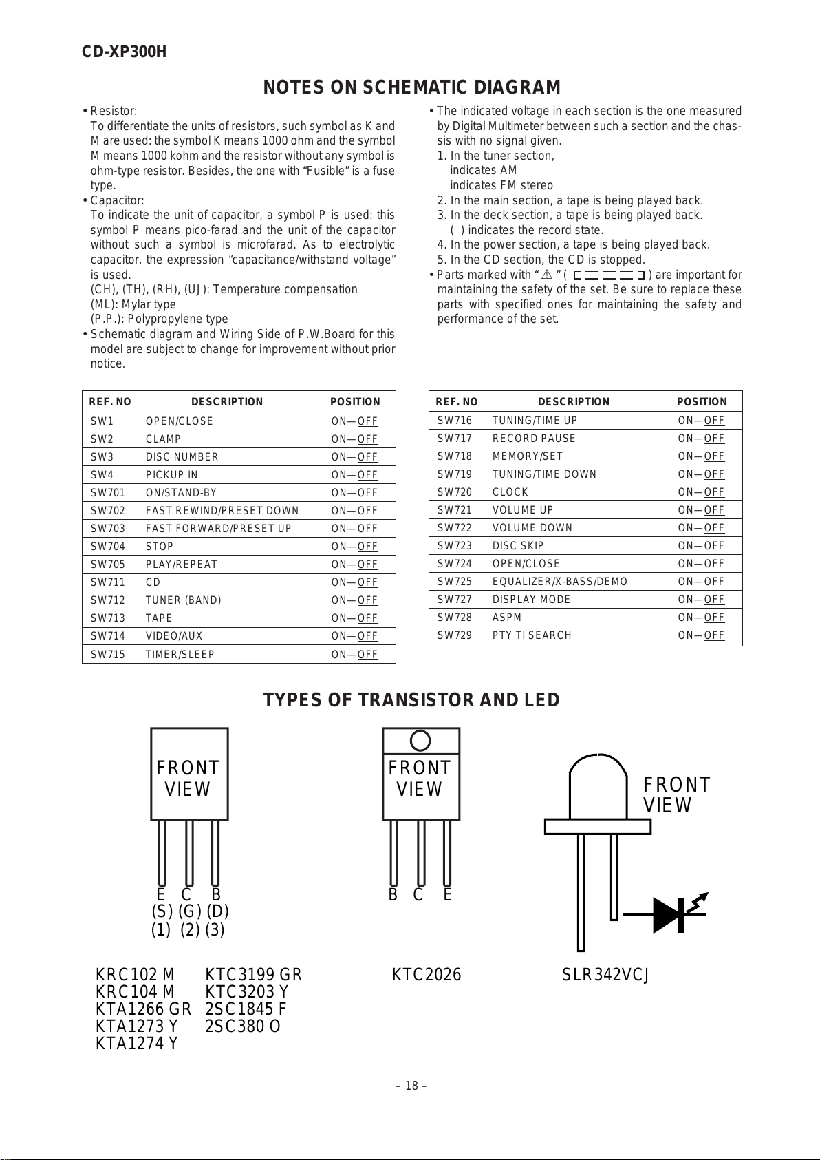
Sharp CD-XP300H User manual

CD-XP300H
No. S2211CDXP300H
CONTENTS Page
SAFETY PRECAUTION FOR SERVICE MANUAL ........................................................................................................... 2
IMPORTANT SERVICE NOTES (FOR U.K. ONLY) .......................................................................................................... 2
SPECIFICATIONS ............................................................................................................................................................. 3
NAMES OF PARTS ........................................................................................................................................................... 4
OPERATION MANUAL ...................................................................................................................................................... 5
QUICK GUIDE (FOR U.K. ONLY)...................................................................................................................................... 8
DISASSEMBLY................................................................................................................................................................ 10
REMOVING AND REINSTALLING THE MAIN PARTS................................................................................................... 13
ADJUSTMENT ................................................................................................................................................................. 14
NOTES ON SCHEMATIC DIAGRAM .............................................................................................................................. 18
TYPES OF TRANSISTOR AND LED............................................................................................................................... 18
BLOCK DIAGRAM ........................................................................................................................................................... 19
SCHEMATIC DIAGRAM / WIRING SIDE OF P.W.BOARD............................................................................................. 22
VOLTAGE ........................................................................................................................................................................ 39
WAVEFORMS OF CD CIRCUIT...................................................................................................................................... 40
TROUBLESHOOTING..................................................................................................................................................... 41
FUNCTION TABLE OF IC................................................................................................................................................ 45
FL DISPLAY..................................................................................................................................................................... 51
WIRING OF PRIMARILY SUPPLY LEADS (FOR U.K. ONLY) ....................................................................................... 52
REPLACEMENT PARTS LIST/EXPLODED VIEW
PACKING METHOD (FOR U.K. ONLY)
SERVICE MANUAL
This document has been published to be used
for after sales service only.
The contents are subject to change without notice.
SHARP CORPORATION
• In the interests of user-safety the set should be restored to its
original condition and only parts identical to those specified be
used.
MINI COMPONENT SYSTEM
MODEL CD-XP300H
CD-XP300H Mini Component System consisting of CD-XP300H
(main unit) and CP-XP300H (speaker system).
• Note for users in U.K.
Recording and playback of any material may require consent
which SHARP is unable to give. Please refer particularly to the
provisions of Copyright Act 1956, the Dramatic and Musical
Performers Protection Act 1956, the Performers Protection Acts
1963 and 1972 and to any subsequent statutory enactments and
orders.
All manuals and user guides at all-guides.com
all-guides.com

CD-XP300H
– 10 –
1 Top Cabinet 1. Screw ...................... (A1) x4 10-1
2 Side Panel 1. Screw ...................... (B1) x8 10-1
(Left/Right)
3 CD Tray Cover/ 1. Turn on the power supply,.. 10-2
CD Player Unit open the disc tray, take out
the CD tray cover, and close.
(Note 1)
2. Screw ...................... (C1) x1
3. Hook........................ (C2) x3
4. Hook........................ (C3) x2
5. Socket ..................... (C4) x2
4 Rear Panel with 1. Screw ...................... (D1) x8 10-2
Fan Motor 2. Socket ..................... (D2) x1
5 Main PWB/ 1. Screw ...................... (E1) x4
10-2, 11-1
RDS PWB 2. Socket ..................... (E2) x3 11-1
3. Flat Cable ............... (E3) x1
4. Flat Wire.................. (E4) x1
6 Front Panel 1. Screw .......................(F1) x2 11-1
2. Hook.........................(F2) x2
3. Socket ......................(F3) x1
7 Display PWB 1. Screw ....................(G1) x12 11-2
2. Flat Cable ............... (G2) x1
8 Tape Mechanism 1. Open the cassette holder. .. 11-2
2. Screw...................... (H1) x5
9
Headphones PWB
1. Screw ....................... (J1) x1 11-2
10 Turntable 1. Hook........................ (K1) x2 11-3
2. Cover ...................... (K2) x1
11 Loading Tray 1.
Turn fully the lock lever in the
10-3
arrow direction
.
2.
Push the loading tray backward
11-4
to engage the claw with the
groove and remove it in the
direction of the arrow
...
(L1) x6
12 CD Servo PWB 1. Screw ......................(M1) x2 11-5
(Note 2) 2. Hook........................(M2) x1
3. Socket .....................(M3) x4
13 CD Mechanism 1. Hook........................ (N1) x2 11-6
2. Hook........................ (N2) x2
DISASSEMBLY
Caution on Disassembly
Follow the below-mentioned notes when disassembling
the unit and reassembling it, to keep it safe and ensure
excellent performance:
1. Take cassette tape and compact disc out of the unit.
2. Be sure to remove the power supply plug from the wall
outlet before starting to disassemble the unit.
3.Take offnylon bands orwire holderswhere they need to
beremovedwhendisassemblingtheunit.Afterservicing
theunit, be sure to rearrangethe leads wherethey were
before disassembling.
4. Take sufficient care on static electricity of integrated
circuits and other circuits when servicing.
Figure 10-2
STEP REMOVAL PROCEDURE FIGURE
Figure 10-1
Note 1: How to open the changer manually. (Fig. 10-3)
1. In this state, turn fully the lock lever in the arrow direction through
the hole on the loading tray bottom.
2. After that, push forward the loading tray.
Note 2:
1. After removing the connector for the optical pickup from the
connector,wraptheconductivealuminiumfoilaroundthefrontend
of the connector so as to protect the optical pickup from electro-
static damage.
Note 3:
1. Be careful not to break the claw of the CD mechanism.
2. When fining back the cam gear assembly, let it lock by front
movement.
CD-XP300H
CD-XP300H
(B1) x 2
ø3 x 10mm
(A1) x 2
ø3 x 12mm
(A1) x 2
ø3 x 12mm
(B1) x 2
ø3 x 10mm
(B1) x 4
ø3 x 10mm
Rear
Panel
Side Panel
(Right)
Side Panel
(Left)
Top Cabinet Front
Panel
(C3) x 1
CD Player
Unit
CD Tray Cover (C2) x 3
1
1
2
(E1) x 1
ø3 x 10mm
(C1) x 1
ø3 x 10mm
(E1) x 1
ø3 x 10mm
(D1) x 1
ø3 x 10mm
Lug Wire
Main PWB
Rear
Panel
Pull
(C3) x 1
(C4) x 2
CD Servo
PWB
Main
PWB
(D2) x 1
(D1) x 7
ø3 x 10mm
Pull
Front
Panel
Figure 10-3
Lock Lever
CD Player Unit
(Bottom View)
All manuals and user guides at all-guides.com

– 11 –
CD-XP300H
Figure 11-1
Figure 11-2
Figure 11-3
Figure 11-4
Figure 11-5
Figure 11-6
(F1) x 2
ø3 x 10mm
Headphones
PWB
(E4) x 1
Front
Panel
(E1) x 2
ø3 x 10mm
(F2) x 1
(F2) x 1
(E2) x 1
(F3) x 1
(E3) x 1
(E2) x 2
Main PWB
Transformer
PWB
RDS PWB
Power PWB
Pull
Pull
Mechanism Dust Cover
(H1) x 5
ø3 x 10mm
Lug Wire
(G2) x 1
(G1) x 12
ø3 x 10mm
Display PWB
Headphones
PWB
Open
Cassette
Holder
Tape Mechanism
(J1) x 1
ø3 x 10mm
Front Panel
CD Player Unit
Loading
Tray
Turntable
(K2) x 1
(K1) x 2
(L1) x 3
3
(L1) x 3 Loading Tray
1
2
CD Player Unit
Loading
Tray
(M1) x 2
ø3 x 10mm
(M3) x 2 CD Servo
PWB
(M2) x 1
(M3) x 2
CD
Mechanism (N2) x 2
(N1) x 1
(N1) x 1 Loading Tray
All manuals and user guides at all-guides.com

CD-XP300H
– 12 –
Figure 12-1 Figure 12-2
1 Woofer 1. Front Panel ............. (A1) x1 12-1
2. Screw ...................... (A2) x4 12-2
2 Tweeter 1. Screw ...................... (B1) x2 12-2
STEP REMOVAL PROCEDURE FIGURE
CP-XP300H
Screwdriver
Driver should
be pried away
from Speaker Box.
(A1) x 1
Speaker Box
(A2) x 4
ø4 x 16mm
(B1) x 2
ø3 x 10mm
Speaker Box
Woofer
Tweeter
All manuals and user guides at all-guides.com

– 13 –
CD-XP300H
REMOVING AND REINSTALLING THE MAIN PARTS
TAPE MECHANISM SECTION
Perform steps 1 to 6 and 8 of the disassembly method to
remove the tape mechanism.
How to remove the record/playback and erase
heads (TAPE 2) (See Fig. 13-1)
1. When you remove the screws (A1) x 2 pcs., the recording/
playback head and three-dimensional head of the erasing
head can be removed.
How to remove the playback head (TAPE 1)
(See Fig. 13-2)
1. When you remove the screws (B1) x 2 pcs., the playback
head can be removed.
How to remove the pinch roller (TAPE 1/2)
(See Fig. 13-3)
1. Carefully bend the pinch roller pawl in the direction of the
arrow <A>, and remove the pinch roller (C1) x 1 pc., in the
direction of the arrow <B>.
Note:
When installing the pinch roller, pay attention to the spring
mounting position.
How to remove the belt (TAPE 2)
(See Fig. 13-4)
1. Remove the main belt (D1) x 1 pc., from the motor side.
2. Remove the FF/REW belt (D2) x 1 pc.
How to remove the belt (TAPE 1)
(See Fig. 13-4)
1. Remove the main belt (E1) x 1 pc., from the motor side.
2. Remove the FF/REW belt (E2) x 1 pc.
How to remove the motor (See Fig. 13-5)
1. Remove the screws (F1) x 2 pcs., to remove the motor.
Figure 13-1
Figure 13-2
Figure 13-3
Figure 13-4Figure 13-5
(A1) x 2
Ø2 x 9mm
TAPE 2
Record/Playback
Head
Erase Head
Clutch Ass'y
(B1) x 2
Ø2 x 9mm
TAPE 1
Playback
Head
Clutch Ass'y
Pinch Roller
(C1) x 1 <A>
<B>
Pinch
Roller
Pawl
Pull
TAPE 2 TAPE 1
Main Belt
(E1) x 1
TAPE 2
Main Belt
(D1) x 1
TAPE 1
Main Belt
(D1) x 1 Main Belt
(E1) x 1
FF/REW
Belt
(D2) x 1
FF/REW
Belt
(E2) x 1
Motor
Motor
(F1) x 2
Ø 2.6 x 5mm
Motor
Clutch Ass'y
All manuals and user guides at all-guides.com

CD-XP300H
– 14 –
How to remove the pickup (See Fig. 14-2)
1. Remove the stop washer (B1) x 1 pc., to remove the gear
(B2) x 1 pc.
2. Remove the screws (B3) x 2 pcs., to remove the shaft
(B4) x 1 pc.
3. Remove the pickup.
Note
After removing the connector for the optical pickup from the
connectorwraptheconductivealuminiumfoilaroundthefront
end of connector so as to protect the optical pickup from
electrostatic damage.
Figure 14-2
CD MECHANISM SECTION
Perform steps 1, 2, 3, 10, 11,12 and 13 of the disassembly
method to remove the CD mechanism.
How to remove the loading motor
(See Fig. 14-1)
1. Bend the hooks (A1) x 6 pcs., to remove the loading motor.
Figure 14-1
ADJUSTMENT
MECHANISM SECTION
•Driving Force Check
Torque Meter Specified Value
Play: TW-2111 Tape 1: Over 80 g
Tape 2: Over 80 g
•Torque Check
Torque Meter
Tape 2
Play: TW-2111 30 to 80 g.cm 30 to 80 g.cm
Fast forward: TW-2231 — 70 to 180 g.cm
Rewind: TW-2231 — 70 to 180 g.cm
Specified Value
Tape 1
Specified
Value
Adjusting
Point Instrument
Connection
Test Tape
Normal MTT-111 Variable 3,000 ±30 Hz Speaker
speed Resistor in Terminal
motor. (Load
resistance:
6 ohms)
•Tape Speed
Figure 14-3
(B3) x 2
ø2.6 x 6mm
Shaft
(B4) x 1
Stop Washer
(B1) x 1
Gear
(B2) x 1
CD Mechanism
Pickup
TAPE MECHANISM
Tape
Motor
Variable Resistor in motor
(A1) x 6
Loading
Motor PWB
Loading
Motor
Loading
Tray
All manuals and user guides at all-guides.com
all-guides.com

– 15 –
CD-XP300H
Figure 15-2
CD ERROR CODE DESCRIPTION
Error Explanation
01 When Pickup set inner position, inner switch
cannot detect 'ON' level for 10 secs.
When tray moves to Open/Close, Open/Close switch
10* cannot detect 'ON' level for 7 secs.
When disc table rotate to target position.
Clamp switch cannot detect 'ON' level for 7 secs.
When disc table set to Disc1 position for 1 st time,
11* "CLAMP SW", "DISC NO SW" and "OPEN/CLOSE"
cannot detect 'ON' level for 14 secs.
31 When it changes to CD function, DSP cannot read
initial data.
T
T
EFBL
FDO
TE
Stopped
CH1=500 mV
DC 10:1 CH2=200 mV
DC 10:1 CH3=1 V
DC 10:1 500 ms/div
(500 ms/div)
NORM:20 kS/s
1
2
3
=Record Length=
Smoothing : ON CH1 : 0.000 V
CH2 : 0.000 V Main : 100 K
Zoom : 2 k Mode : SINGLE
Type : EDGE CH1
Delay : 0.0 ns
Hold off : 0.2 µs
CH3 : 0.00 V
CH4 : 0.00 V
BW : FULL
=Trigger==Filter= =Offset=
CH2
v/DIV
200 mV
1999/04/05 20:26:47
Test Stage Frequency Frequency
Display Setting/
Adjusting
Parts
Instrument
Connection
CD SECTION
• AM IF/RF
Signal generator: 400 Hz, 30%, AM modulated
*1. Input: Antenna Output: TP302
*2. Input: Antenna Output: TP301
TUNER SECTION
fL: Low-range frequency
fH: High-range frequency
AM IF 450 kHz 1,620 kHz T351 *1
AM Band — 522 kHz (fL): T306 *2
Coverage 1.1 ±0.1 V
AM Tracking 990 kHz 990 kHz (fL): T303 *1
Figure 15-1 ADJUSTMENT POINTS
Items adjusted automatically
(1)Offset adjustment (The offsetvoltage between the head
amplifier output and the VREF reference voltage is
compensated inside the IC.)
* Focus offset adjustment
* Tracking offset adjustment
(2) Tracking balance adjustment (waveform drawing
Fig.15-2 EFBL)
(3)Gainadjustment(ThegainiscompensatedinsidetheIC
sothat the loop gain atthe gain crossoverfrequency will
be 0 dB.)
* Focus gain adjustment
* Tracking gain adjustment
•Adjustment
Since this CD system incorporates the following automatic
adjustment functions, readjustment is not needed when
replacingthe pickup. Therefore,differentPWBsandpickups
can be combined freely.
Each time a disc is changed, these adjustments are
performed automatically. Therefore, playback of each disc
can be performed under optimum conditions.
AM IF
TP301
TP302
R381
R357
T303
T306
L354
T351
CNP301
AM LOOP
ANTENNA
AM BAND
COVERAGE fL AM TRACKING
fL
MAIN PWB
FE301
SO301
FM ANTENNA
TERMINAL
* 'CHECKING'
IfErrorisdetected,'CHECKING'willbedisplayinsteadof'ER-
CD**' display. 'ER-CD**' display will only be display when
error had been detected for the 5 th times.
• FM IF
Notes:
1: Description of the "FM IF Adjustment" is not carried on this
Manual. It is because the IF coil in the FM front end section
has been best adjusted in the factory so that its further
adjustment is not needed at the field. When replacing the
FM front end assembly, no adjustment is needed either.
2: The parts in the FM front end section are prepared in a
complete unit, so you can't obtain each part individually.
All manuals and user guides at all-guides.com

CD-XP300H
– 16 –
TEST MODE
•Setting the test mode
Any one of test mode can be set by pressing several keys as follows.
<X-BASS> + <CD> + <POWER> TEST: CD operation test.
Function: -CD test mode.
-Enter test mode.
C D T E S T
OPEN/CLOSE operation is using manual.
<< >>, << >> buttons make pick's slide possible.
Do TOC IL. Do normal play.
When these following key is input
into PLAY key, track number can
be appoint directly.
<<PLAY>> key input. <<MEMORY>> key input.
<< 1>> key: Track 4
<< 2>> key: Track 9
<< 3>> key: Track 15
<<STOP>> key input.
STOP
Laser ON.
<<MEMORY>> key input.
Tracking OFF play at that
specific point.
<<MEMORY>> key input.
Tracking ON play from
that specific point.
<<STOP>> key input.
STOP
IL isn't done
VOL — Last memory
BAL — CENTER
P.GEQ — FLAT
X-BASS — OFF
To cancel : Power OFF
Sliding the PICKUP with
<< >>, << >> button
must only be in STOP mode.
<<MEMORY>>
key input.
Adjustment result
automatically will
display as below.
for each 2 sec :
a) "FOFF_XX"
b) "TOFF_XX"
c) "TBAL_XX"
d) "TGAN_XX"
f) "FGAN_XX"
g) "RFLS_XX"
explanation:
a) Focus off set = "FOFF_XX"
b) Tracking off set = "TOFF_XX"
c) Tracking balance = "TBAL_XX"
d) Tracking Gain = "TGAN_XX"
f) Focus Gain = "FGAN_XX"
g) RF level shift = "RFLS_XX"
Adjustmentresultautomaticallywill
display as below for each 2 sec :
a) "FOFF_XX"
b) "TOFF_XX"
c) "TBAL_XX"
d) "TGAN_XX"
f) "FGAN_XX"
g) "RFLS_XX"
<<MEMORY>> key input.
All manuals and user guides at all-guides.com

– 17 –
CD-XP300H
Standard Specification of Stereo System Error Message Display Contents
Error Contents DISPLAY Notes
TAPE Mechanism Error. 'ER-TA**' 00: Tape Mechanism Error.
01: Initial Error.
02:
03:
CD Pickup Mechanism Error. 'ER-CD**' 01: PU-IN SW Detection NG.
02:
03:
04:
CD Changer Mechanism Error. 'ER-CD**' 10: Changer Error.
(*) 11: Initial Error.
12:
13:
CD DSP Communication Error 'ER-CD**' 31: DSP COMMUNICATION ERROR
Focus Not Match. 'NO DISC'
IL Time Over. 'NOT READ'
TUN PLL Unlock. 'ER-TU**' 00: TUN Error.
01: PLL Unlock.
02:
03:
(*) CHECKING:
IfCDchangermechanismerrorisdetected,'CHECKING'willbe display instead of'ER-CD**'display'ER-CD**'willonlybedisplay
when CD changer mechanism error had been detected for the 5 th times.
Speaker abnormal detection and +B PROTECTION display
In case speaker abnormal detection or +B PROTECTION had occurred, it can be check by pressing 'POWER', 'VIDEO' and 'X-
BASS' key twice. Display will show "S** B**". S is referring to speaker abnormal detection and B is referring to +B PROTECTION.
** is in hex valve.
+B PROTECTION is condition when irregular process occur on power supply line.
All manuals and user guides at all-guides.com

CD-XP300H
– 18 –
•The indicated voltage in each section is the one measured
by Digital Multimeter between such a section and the chas-
sis with no signal given.
1. In the tuner section,
indicates AM
indicates FM stereo
2. In the main section, a tape is being played back.
3. In the deck section, a tape is being played back.
( ) indicates the record state.
4. In the power section, a tape is being played back.
5. In the CD section, the CD is stopped.
•Parts marked with “ 1” ( ) are important for
maintaining the safety of the set. Be sure to replace these
parts with specified ones for maintaining the safety and
performance of the set.
NOTES ON SCHEMATIC DIAGRAM
•Resistor:
To differentiate the units of resistors, such symbol as K and
M are used: the symbol K means 1000 ohm and the symbol
M means 1000 kohm and the resistor without any symbol is
ohm-type resistor. Besides, the one with “Fusible” is a fuse
type.
•Capacitor:
To indicate the unit of capacitor, a symbol P is used: this
symbol P means pico-farad and the unit of the capacitor
without such a symbol is microfarad. As to electrolytic
capacitor, the expression “capacitance/withstand voltage”
is used.
(CH), (TH), (RH), (UJ): Temperature compensation
(ML): Mylar type
(P.P.): Polypropylene type
•Schematic diagram and Wiring Side of P.W.Board for this
model are subject to change for improvement without prior
notice.
REF. NO DESCRIPTION POSITION
SW716 TUNING/TIME UP ON—OFF
SW717 RECORD PAUSE ON—OFF
SW718 MEMORY/SET ON—OFF
SW719 TUNING/TIME DOWN ON—OFF
SW720 CLOCK ON—OFF
SW721 VOLUME UP ON—OFF
SW722 VOLUME DOWN ON—OFF
SW723 DISC SKIP ON—OFF
SW724 OPEN/CLOSE ON—OFF
SW725 EQUALIZER/X-BASS/DEMO ON—OFF
SW727 DISPLAY MODE ON—OFF
SW728 ASPM ON—OFF
SW729 PTY TI SEARCH ON—OFF
SW1 OPEN/CLOSE ON—OFF
SW2 CLAMP ON—OFF
SW3 DISC NUMBER ON—OFF
SW4 PICKUP IN ON—OFF
SW701 ON/STAND-BY ON—OFF
SW702 FAST REWIND/PRESET DOWN ON—OFF
SW703 FAST FORWARD/PRESET UP ON—OFF
SW704 STOP ON—OFF
SW705 PLAY/REPEAT ON—OFF
SW711
CD
ON—OFF
SW712 TUNER (BAND) ON—OFF
SW713 TAPE ON—OFF
SW714 VIDEO/AUX ON—OFF
SW715 TIMER/SLEEP ON—OFF
TYPES OF TRANSISTOR AND LED
REF. NO DESCRIPTION POSITION
(1) (2) (3)
(S) (G) (D)
E C B
FRONT
VIEW
B C E
FRONT
VIEW
KRC102 M
KRC104 M
KTA1266 GR
KTA1273 Y
KTA1274 Y
SLR342VCJKTC2026
FRONT
VIEW
KTC3199 GR
KTC3203 Y
2SC1845 F
2SC380 O
All manuals and user guides at all-guides.com

– 19 –
CD-XP300H
Figure 19 BLOCK DIAGRAM (1/3)
+5V
(+B7)
CNS4
BI4
CNP4
M3
CD LOADING
MOTOR
+–
+3.3V(+B11)
TO DISPLAY SECTION
TO MAIN SECTION
CONSTANT
VOLTAGE
Q2
LASER
DRIVER
+3.3V(+B11)
Q1
+5V
(+B7)
PICKUP UNIT
IC1
LC78645NE
CD SERVO
VDD
LDD
LDS
M
SW3
DISC
NUMBER
SW2
CLAMP
SW1
OPEN/
CLOSE
CNP8
CNP7
TRACKING COIL
FOCUS COIL
SW4
PICKUP
IN
M2
SLED
MOTOR
M1
SPINDLE
MOTOR
M
M
Q3
XVDD
RVDD
LVDD
RFVDD
XL1
33.8688 MHz
O/C
CLAMP SW
CD RES
CL
DI
DO
CE
DRF
WRQ
+6.5V (+B4)
D_GND (DRIVER)
+5V (+B8)
VCC3
VCC2
VCC4
VCC1
IC2
M63001FP
FOCUS/TRACKING/
SPIN/SLED
DRIVER
XIN
XOUT
RES
WRQ
DO
DI
CLK
CE
TIN2 F
TIN1 E
FIN2 B
FIN1 A
TDO
FDO
SPDO
SLDO
CONT5
CONT2
CONT3
CONT4
VDD5
LCHO
RCHO
80
79
75
20
5
40
18
24
23 14
8
21
22
29
35
41
47 46
38
VVDD
77 10
987
15
1
2
17
25
42 41 39 38
4765 16
28
26 27
316452
316452
316452
54
71
61
62
63 69
57
56
55
51
50
43
44
40
37
19
28
26
23
22
21
327168910
687
+5V (+B7)
D_GND
L-CH
35
4
A_GND
R-CH
12
4245 68 25 70
64
65
66
DRF
67
48
49
ADAVDD
18
+3.3V
(+B11)
DISC NO
~~
ZD1
3.3V
+
–
–
+
All manuals and user guides at all-guides.com
all-guides.com

CD-XP300H
– 20 –
Figure 20 BLOCK DIAGRAM (2/3)
+B6
7
8
6
5
4
+B4
IC101
AN7345K
PLAYBACK AND RECORD
/PLAYBACK AMP.
AUX L
R
JK690
VIDEO/AUX IN
VCC
+B5
CLK
+B6
+B6
+B6 +B5
AM IF
VT
AM LOOP
ANTENNA
CNP301
BI601
–20dB
ATT
Q101~
Q104
Q107
Q108
Q601
Q602 Q603
Q604
10.7 MHz
450 kHz
REC/PLAY
CLK
CE
DI
DO
DI
CE
MO/ST
SWITCHING
+B5
FM/AM
IC302
LC72131
PLL
(TUNER)
FM/AM
OUT
R
L
BIAS
T1/T2
MUTING
P.B. REC.
AC BIAS
TAPE
TUNER
CD
PB
CNP7
FROM
CD SERVO
SECTION
HEAD
ERASE
SWITCHING
SWITCHING
SWITCHING
BIAS
Q113
Q114
Q112
Q110
Q706
Q707
Q708
SWITCHING
Q109
BIAS OSC
Q111
L103
Q105
Q106
RECORD/
PLAYBACK
HEAD
TAPE 2
PLAYBACK
HEAD
TAPE 1
L-CH
R-CH
L-CH
R-CH
IC601
LC75341
AUDIO
PROCESSOR
+B5
R
L
REC
R
L
ALC
R REC
L REC
POP
REDUCE
SWITCHING
L(T2)
R(T2)
R(T1)
L(T1)
+B7
+B8
R
L
PHASE
(FM/AM)
MPX IN
STEREO
AM RF IN
AM OSC IN
AM OSC OUT
FM
Q360
X OUT
X352
4.5 MHZ
AM BAND
COVERAGE
AM
TRACKING
T303 T306
X351
456 kHz
ZD351
5.1V
MO/ST
VCO
FM
DET
FM+B
GND
AM IF
CF351
IC303
LA1832S
FM IF DET.
FM MPX./AM IF
AM MIX
CF352
T351
CF302
CF301
Q301
FE301
FM FRONT END
21
4
24
2
1
81817
3
9
10
18
11
16
3
15
10
9
7
23
14
12
13
1
2
19
7
18
10
13
21
4
2
24
23
6
9
16
12
11
15
1
5413
7
2
4
1
21
7
985
17
6
21
21
20 22 11
17
1615
5
1
63
13
14
12
15
162324
4
7
H/N
P.B
REC
T1/T2
T1/T2
ALC
+B5
+B5
+B5
SYSTEM
MUTE
TAPE
MECHANISM
ASS'Y
MOTOR
DRIVER
SOLENOID
DRIVER
+B3
+B3
ICT21
LC72723
RDS DEORDER
16
15
14
13
8
9
10
2
3
11
7
SO301A
FM ANTENNA
TERMINAL
MPX IN VDDA
X OUT
X IN
QT21
XT21
4.332 MHz
RST
RDDA
RDCL
RD-ID/
READY
AOUT
X IN
L354
LOW PASS LOW
FM IF
AMP.
R
L
+B5
VSSD
TEST
L
R
L
R
L
R
L
R
VDDD
All manuals and user guides at all-guides.com

– 21 –
CD-XP300H
Figure 21 BLOCK DIAGRAM (3/3)
KIA7805AP
AN78L05
Q905
–VF
VF2
VF1
Q801
IC855
+B2
+B3
+B4
-B1
+B1
-B2
+B7
+B3
+B10
-
12 13 41
+B5
19
Q705
R
L
2
0dB
T
T
+B10
RX701
REMOTE
SENSOR
D803, D804
D802
D801
RL914
JK701
HEADPHONES
M4
FAN
MOTOR
M
Q906
Q709
Q601
Q602 Q603
Q604
IC901
STK41221
POWER AMP.
F804
T2A L 250V
VOLTAGE
REGULATOR
F803
T2A L 250V F805
T2.5A L 250V
F802
T4A L 125V
F801
T4A L 125V
R-OUT
L-OUT
Q901~
Q904
CLK
SO901
SPEAKER
TERMINAL
AC POWER
SUPPLY CORD
AC 230 V, 50 Hz
32
REC/PLAY
VLOAD
RESET
+B10 +B10
+B10
+B10
+B9
VDD VDD
VDD
~
CE
DI
DO
XL700
4.194304 MHz
–
BIAS
T1/T2
AVDD
SW701~SW705
SW711~SW725
SW727~SW729
KEY
TO CD
SERVO
SECTION
TO CD
SECTION
IC701
IX0524AW
SYSTEM
MICROCOMPUTER
FL701
FL DISPLAY
z
27
85
80
33 45
93
14
92
1245678
14
18
2
78
70
51
3
2
1
11
6
71
58
100
33
31
37
26
15
46
1112
9
10 16 17 20 21222324
41
79
543859 62
~
5245 51 50
55 49
48 40 25 13
39
34
T.F.
PT801
MAIN POWER
TRANSFORMER
SYSTEM
MUTE
~
~~
91
86
~
~~~
TAPE
MECHANISM
ASS'Y
RESET
SP DET.
SP RELAY
ON-OFF
FAN MOTOR
DRIVER
IC851
IC852
IC853
IC854
M_+13V
LD+7V
+B5
+B10
A+10V
UNSW_5.6V
+B7
+B8
+B9
D_5V
A_5V
SW_5V
KIA7810AP
KIA7812AP
IC851~IC854
VOLTAGE REGULATOR
VOLTAGE
REGULATOR
M
L841
LINE
FILTER
RL841
PT841
SUB POWER
TRANSFORMER
D842~
D845
+B10
All manuals and user guides at all-guides.com

CD-XP300H
– 22 –
Figure 22 SCHEMATIC DIAGRAM (1/10)
A
B
C
D
E
F
G
H
123456
• NOTES ON SCHEMATIC DIAGRAM can be found on page 18.
9.3V 8.6V
9.3V
0V 3.4V
3.4V
0V
0V
0V
0V
0V
0.7V
0.7V
0.7V
0V
0V
0V
0.7V
0V
0V
0V
0V 0V
0V
0V 0.7V 0.7V
1
23
3
2
7
6
5
4
3
2
1
3
2
1
FM SIGNAL
PLAYBACK SIGNAL
RECORD SIGNAL
CD SIGNAL
VIDEO SIGNAL
CNP7
R602 1K
24
23
22
21
20
19
18
17
16
15
14
13
12
11
10
9
8
7
6
5
4
3
2
1
24 23 22 21
1 2 3 4
181920
5 6 7
131415
1617
8 9
10 11 12
R_CH
L_CH
A_GND
CD_D_GND
CD_A_GND
D_GND
(DRIVE)
LD+7V
A_5V
D_5V
REC_R
D_GND(DRIVE)
LD+7V
A_5V
A_GND
L
L
R
R
TO POWER SECTION
P26 1 - F
TO CD
SERVO
PWB
P31 12 - D D_5V
D_GND
L-CH
A_GND
R-CH
T1_R
T1_L
A_GND
M_GND
ERASE
T2_R2
T2_R1
T2_L1
T2_L2
ERASE
HEAD
TAPE2
RECORD/
PLAYBACK
HEAD
TAPE 1
PLAYBACK
HEAD
R-CH
L-CH
R-CH
L-CH
8 8
7
1
7
7
6
5
4
3
2
1
3
2
1
4
6
5
3
2
6
5
4
3
2
1
–
+
CCB
INTERFACE
AUX
DECK
TUNER
CD
112K 56K
112K 56K
Hich=CHROME
+
Hich=T1
–
+
–
Nor/CrO2
RIPPLE
ALC
ALC
Vcc
LSEL0
R1
R2
R3
R4
RSEL0
RIN
RTRE
RBASS
ROUT
VREF
VDD
CLK
L1
L2
L3
L4
LIN
LTRE
LBASS
LOUT
VSS
CE
DI
–
+ –
+
–
+ –
+
–
+
–
+
–
+
+
–
+
–
8
20
3
2
1
14
11
12
19
Q101-106:SWITCHING
Q112-114:
SWITCHING
Q603,604:
SYSTEM MUTE
+B
+B
+B
BI601
R619
330
R618
330
Q604
KTC3199 GR Q603
KTC3199 GR
R617
2.2K
C637
0.001
C638
0.001
R616
2.2K
R615
3.3K
Q601
KTC3199 GR
R613
390
R611
2.2K
C635
0.001
C636
0.001
R614
3.3K
Q602
KTC3199 GR
R610
2.2K
R612
390
R605 10K C609 1/50
C607
0.1
R607 3.9K
C611 0.0022 C605
0.1
C613 1/50
C615 4.7/50
C617 1/50
C619 1/50
C621 1/50
C623
1/50
IC601
LC75341
AUDIO PROCESSOR
C651
220P
C652
220P
R601 1K
C653
220P C601
220/16
C
6
0.
C603 22/50
C608
0.1
C606
0.1 C
6
0.
0
C614 1/50
C616 4.7/50
C618 1/50
C620 1/50
C622 1/50
C624 1/50
CNP101
CNP102
C640
1/50 R620
22K C639
1/50
R621
22K
C625
0.0022
R609
1.2K
R149 150
C141
100/16
Q113
KRC104 M
Q112
KTA1266 GR
R146
10K R147
10K
R148
4.7K
Q114
KRC104 M
R101 1K
R102 1K
R112 15K
C102
560P
C101
560P
Q102
2SC1845 F
C104
180P
Q104
2SC1845 F
R106
3.3K
R104
2.2K
C103
180P
R105
3.3K
Q103
2SC1845 F
Q101
2SC1845 F
R103
2.2K
R109
4.7K
R107
47K
Q105
KTC3199 GR
C105
560P
R110
4.7K
Q106
KTC3199 GR C106
560P
R108
47K
R116
56
C112
100/16
C114
0.033
C116
560P
R118
100K R120
3.9K
C118
47/25
R124
5.6K
R114
1K C110
330P
C108
330P
R113 1K C109
330P
C107
330P
R122
12K
C120
0.0022 R126
4.7K
R150
68K
R128
5.6K
C124 270P
R138
10K
Q108
KTC3199 GR
Q10
7
KTC319
9
R139
10K
R13
220
K
C626
0.0022 R608
1.2K
R130 1.5K
R132
100
C128
0.022 C130
0.0033
R134
10K
C132
47/25
C133 22/50
C134 220/10
C135 0.022
C131
47/25
C125
22/50
R135
10K
R131 1.5K
C127 0.022
C129 0.0033
R133
100
C123
270P
C121
0.022
R127
4.7K
C119
0.0022
C143
3.3/50
R129
5.6K
R123
5.6K
C115
560P
R115
56
C111
100/16
C113
0.033
R117
100K
R119
3.9K
C117
47/25
R111 15K
C126
22/50
IC101
R121
12K
IC101
AN7345K
PLAYBACK AND
RECORD/
PLAYBACK AMP.
CNS601
All manuals and user guides at all-guides.com

– 23 –
CD-XP300H
Figure 23 SCHEMATIC DIAGRAM (2/10)
78 9 10 11 12
0.7V
0V
0V
11.6V
11.6V 0V
0V
0V 0V
TO
DISPLAY
PWB
P28 1 - E
27
1
FFC701
CNP701
0
2 1K
R603 1K
4
3
2
1
0
9
8
7
6
5
4
3
131415
16
9 10 11 12
A+10V
D_GND
UNSW_5.6V
M_GND
TAPE_A_GND
A_GND(A-PRO)
D_GND
CE
A+10V
M_+13V
SP_RLY
SP_DET
TUN_L
SW_5V
RDS_READY
RDS_RDCL
RDS_RDDA
RDS_RST
TUN_SM
DO
CLK
DI
TUN_R
A_GND
+B_PROTECT
REC_R
SPAN
MIC IN
KARAOKE LATCH
TO POWER SECTION
P26 1 - F
UNSW_5.6V
SW_5V
S_MUTE
A+10V
M_+13V
LVL_DET
TO TUNER SECTION
P25 8 - G
+B_PROTECT
RDS_READY
RDS_RDCL
RDS_RDDA
RDS_RST
–20dB
SP_DET
D_GND
SP_RLY
REC/PLAY
T_T1/T2
T_BIAS
CLK
DI
TUN_SM
CE
DO
R-CH
L-CH
9
10
11
12
13
14
15
16
17
18
19
20
21
22
23
24
25
26
27
8
7
6
5
4
3
2
1
56K
5
6K
M
E
Nor/CrO2
RIPPLE
ALC
ALC
Vcc
MAIN PWB-A1 (1/3)
CHASSIS
GND
17 64151371810916
21
1
23
SWITCHING
BIAS
OSC
BIAS
+B
+B
+B
+B
+B
+B
+B
+B
+B
31
32
33
34
35
25
30
27
22
26
28
23
24
29
JK690
VIDEO/
AUX IN
R693
33K
R692
33K
R690
6.8K C690
390P
R691
6.8K C691
390P
CNP601
3
P
C601
220/16
C602
0.022
C603 22/50
C608
0.1
R604
10K
C610
1/50
C606
0.1
R606
3.9K
C612
0.0022
C614 1/50
C616 4.7/50
C618 1/50
C620 1/50
C622 1/50
C624 1/50
3
8
K
GR
Q107
KTC3199 GR
R139
10K
R136
220K R137
220K
R641 10K
R643
22K
R644
22K
R642 10K
6
0
22 R608
1.2K
C130
0.0033
R134
10K
C132
47/25
C133 22/50
C134 220/10
C135 0.022
R158
220
Q109
KTA1266 GR
R140
47K Q110
KRC104 M
R141
4.7K
R142
82
(1/2W)
Q111
KTC3203 Y
R145
4.7
C137
0.047
(ML)
R143
47K
R144
22K
C131
47/25
R135
10K
C129
0
.
0033
C140
47/25
L103
330 µH
C139
0.039
(ML)
C138
0.0082
(P.P.)
All manuals and user guides at all-guides.com

CD-XP300H
– 24 –
A
B
C
D
E
F
G
H
123456
• NOTES ON SCHEMATIC DIAGRAM can be found on page 18.
Figure 24 SCHEMATIC DIAGRAM (3/10)
FM SIGNAL
AM SIGNAL
123 456 78 9
10 11
1
4
15161718192021222324
12345678
123456789
10 11
1213141516171819202122
TP301
TP302
CONT
IF
FM/AM
FM/AM
SD
ST IND
MO/ST
F OUT
IF OUT
VCC
VT
GND
GND
GND
ANT
VSS
AOUT
AIN
PD
VDD
FM IN
AM IN
DO
CLK
DI
CE
X IN
X OUT
IF IN
REG
AM IF IN
GND
SD
STEREO
FM DET
VCC
IF OUT
PHASE
L CH OUT
R-CH OUT
MPX IN
MPX VCO
FM/AM OUT
VSM
AM LOW CUT
AM RF IN
AM OSC IN
FM AFC
AM OSC OUT
AM MIX OUT
FM IF IN
AM LOOP
ANTENNA
1
AM ANTENNA
AM TRACKING
2
21
AM OSC.
AM BAND
COVERAGE fL
CHASSIS
GND
CHASSIS
GND
+B
+B +B
31
2
1
2
3
AM IF
FM IF AMP.
3.9K
0.022
SO301A
FM
ANTENNA
TERMINAL
R369 15
L342
2.2 µHC341
0.022
R347
6.8K
R346
330
Q301
2SC380 O
R378 1K
R372 1K
R374 1K
R373 1K
R359
C386
330P R395
47K
R376
1K
R386
22K
R360
4.7K
C383
47P
C382
15P(CH)
X352
4.5 MHz
C381
12P(CH)
R344 470
R399
33
C348
0.01
C347 0.022
CF301
R349 33
R348
680
R345 4.7K
C346 0.022
C321 100/16
C345 0.022
FE301
FM FRONT END
C397
0.022
R382
150 R381
10K
C392
0.001
R380
1.5K
C393
1/50
R379
2.2K
C380
10/50
C394
47/25
C387
0.022
C385
0.01
L351
100 µHR377
47K
R387
5.6K
C399
0.022
C398
100/10
R393
1K
R388
C358
1/50
C356
0.001
C355
22P
C357
2.2/50
R353
270
C353
0.022
CF352
T351
C354 0.022
CF351
R352
1K
C351 0.022 R351 5.6K
C350 0.022
C352 10/50
CF302
D302
DS1SS133
D301
DS1SS133
C338
0.001
L341
C334
22P
(CH)
C323
0.022
CNP301
C302 0.001
T303
R323
68K
VD301
SVC348S
T306
C330
15P
C331
0.047
C332
0.022
C335
560P
R336
10K
C366 0.001
C362 3.3/50
C361 0.022
C363 0.022
C364 2.2/50
R365
10K
C365 0.022
C342
R358
3.9K R350
2.7K X351
456 kHz
L354
LOWPASSFILTER
C368
1/50
C367
1/50
R357
470K
R356
1K
C374 0.015
C369
27P
(UJ)
IC302
LC72131
PLL(TUNER)
C389
0.001
All manuals and user guides at all-guides.com
all-guides.com

– 25 –
CD-XP300H
Figure 25 SCHEMATIC DIAGRAM (4/10)
78 9 10 11 12
TO MAIN SECTION
P23 12 - C
1
2
3
4
5
6
7
8
9
10
11
12
13
14
15
16
89
10 11 12
1314151617
TUN_R
TUN_L
TUN_SM
RDS_RST
RDS_RDDA
RDS_RDCL
RDS_READY
A_GND
D_GND
A+10V
DO
CLK
DI
CE
RDS PWB-A4
XOUT
TEST
CIN
FLOUT
VSSA
VDDA
MPXIN
XIN
READY
RDS-ID/
RDCL
RDDA
RST
MODE
VDDD
VSSD
VREF
TP302
TUNER PWB-A1 (2/3)
MO/ST
FM DET
VCC
IF OUT
PHASE
(FM/AM)
PHASE L-CH OUT
R-CH OUT
MPX IN
MPX VCO
1
2
3
4
5
6
7
1
2
3
4
5
6
7
+B
+B
+B
+B
+B
22 35343332313029282726252423
3.9K
1/50
CNS303
CNP303
C388
0.001
R384
5.6K
RT22
390 RT23
390
C391
47/25
R383
5.6K
R392
270
R385
5.6K
Q360
KTA1266 GR R391
270
C395 0.022
C396
100/10
R359
1.8K
ZD351
DZ5.1BSB
L352
100 µH
C384
0.001
R395
47K
R386
22K
R360
4.7K
7
7
K
R387
5.6K
C399
0.022
C398
100/10
3
R388
ZDT21
DZ5.1BSB
RT30 1K
LT21
2.2 µH
CT24
47/25
LT22
2.2 µH
CT30 0.022
CT27
0.022
CT32
47/25
CT31
47/25
CT28
0.022
CT26
560P
RT26
56K
RT25
10K QT21
KTC3199 GR
RT24
56K
CT29
0.022
CT25
22P
(CH)
XT21 4.332 MHz
CT22
0.022
CT21
47/25
RT21
10K
RT29
1K
RT28
1K
RT27
1K
CT23
22P(CH)
RT31
10K
C358
1/50
C356
0.001
C355
22P
R355
3.3K
C370
C357
2.2/50
R353
270
CF351
X351
56 kHz
F
ILTER
C368
1/50 R357
470K
C373
0.015
R356
1K
C374 0.015
C369
27P
(UJ)
C371 1/50
C372
1/50
IC303
LA1832S
FM IF DET./FM
MPX./AM IF
ICT21
LC72723
RT32
6.8K
ICT21:
RDS DECORDER
R370
1K
All manuals and user guides at all-guides.com

CD-XP300H
– 26 –
Figure 26 SCHEMATIC DIAGRAM (5/10)
A
B
C
D
E
F
G
H
123456
• NOTES ON SCHEMATIC DIAGRAM can be found on page 18.
18V
13 V
3 1
3 1
3 1
3 1
2
2
2
2
18 17 16 15 14 13 12 11 10 9 8 7 6 5 4 3 2 1
CD_D_GND(DRIVE)
CD_A_GND
TAPE_A_GND
L_CH
A_GND
+B_PROTECT
+B
SP_RLY
R-CH
A+10V
SP_DET
A_5V
LD+7V
SW_5V
D_5V
M_+13V
D_GND
M_GND
A_GND (A-PRO)
TO
DISPLAY P
W
P29 12 - D
UNSW_ 5.6V
CD_D_GND
VH+
VH– VL– VL+
SP_DET
TO MAIN SECTION
P22 1 - C,P23 9 - H
1
2
3
4
5
6
7
8
9
10
1111
10
9
8
7
6
5
4
3
2
1
–
+
–
+
8
1
7
6
2
3
4
16
21
20
19
18
17
15
14
13
12
11
10
9
+B
+B
+B
+B
+B
+B
+B
+B
+B
-B
-B
-B
-B
-B
-B
-B
-B
+B
+B
+B
+B
+B
+B
+B
+B
+B
+B
0.29 µH
IC901
STK41221
POWER AMP.
C905
22/50
R907
56K
C908
3.3P(CH)
C907
100P
R903 1K
R912
100
Fusible
(1/4W)
R913
0.22(3W)
R916
0.22(3W)
C913
100P
R904
1K
R905
560
R906
560
C906
22/50
C909
0.1/50
R909
33K C910
3.3P(CH)
R911 56K
C912
100/100
C914
100/100
R910
1K
R918
1.5K
R917
0.1(3W)
C917
0.022(ML)
Q902
KTC3199 GR
D906
DS1SS133
R919
1.8K
C916
100/50
C918 100/50
ZD902
DZ150BSB
R925
1.5K
ZD903
DZ15BSB
R926
1.5K
D907 DS1SS133
Q904
KTC3199 GR
Q903
KTC3199 GR
C925
47/50
R937
56K
R934
56K
L902
R935
56K
Q901
KTC3199 GR
D905
DS1SS133
R920
1.8K
C919
0.022
(ML)
R921
1.5K
R922
0.1(3W)
R908
1K
R958
100
Fusible
(1/4W)
C915
100/100
C911
100/100
C904
220P
C903
220P
R902
56K
R901
56K
C902
0.22/50
C901
0.22/50
R928
22K
R927 22K
C923
3300/71
C922
4700/35
C920
3300/71
C921
4700/35
R929
47K
D909
DS1N404S
R930
47K
D910
DS1N404S
L901
0.29 µH
CNP
8
CNS8
0
BI801
LG1
CHASSIS
G
C856
3300/35
IC851
KIA7812AP
VOLTAGE
REGULATOR
C864
0.1
(ML)
D858
DS1SS133
D859
DS1SS133
C852 22/50
R854 22K
C851 0.047
(ML)
R860
220
C865
10/50
ZD852
DZ8.2BSB
D857
DS1SS133
R859 22K
C863
22/50
IC855
KTC2026
SILICON
D852
DS1SS133
D851
DS1SS133 R853
22K
IC852,853:
VOLTAGE REGULATOR
C855
0.1(ML)
C853
47/25
C854
0.1
(ML)
IC853
KIA7805AP
C857
47/25 C858
0.022 C859
0.1(ML)
R852
10K
D853
DS1N404S
R858 220
D855
DS1SS133
IC854
AN78L05
VOLTAGE REGULATOR C862
10/50
C861
0.047
(ML)
C860
47/25
D856
DS1SS133
IC852
KIA7810AP
LG2
CHASSIS GND
CNS705
All manuals and user guides at all-guides.com

– 27 –
CD-XP300H
Figure 27 SCHEMATIC DIAGRAM (6/10)
78 9 10 11 12
4.4 V
0.2 V
1
2
AC_RLY
VF1
P_IN
–VF
VF2
R
L
R
L
TO
DISPLAY PWB
P29 12 - D
L-CH
GND
R-CH
SP_RLY
M_+13.5V
SUB_B
L-CH
R-CH
L-CH GND
R-CH GND
–
+
VL–
VL+
VH–
VH+
R1_OUT
L1_OUT
1
2
3
4
5
6
7
8
9
10
11
4
5
1
6
7
8
9
2
3
11
10
11
10
5
4
3
2
1
5
4
3
2
1
M
1
2
9
8
7
6
5
4
3
2
1
AMP. PWB-A1 (3/3)
POWER PWB-A3
+
–
–
+
HEADPHONES
PWB-B2
TRANSFORMER PWB-A2
5
1
+B
+B
+B
-B
-B
-B
-B
+B
B
+B
+B
FAN
MOTOR
DRIVER
+B
+B
+B
11
44
0.29 µH
Q903
KTC3199 GR
C925
47/50
R937
56K
R934
56K
L902
R935
56K
0
4S
L901
0.29 µH
C927
0.22
C929
0.22
R939 10(1/2W)
R940 10(1/2W)
R941
10
(1/2W)
C926
0.22
C928
0.22
R938
10
(1/2W)
Q905
KTC3199 GR
SP RELAY
ON-OFF R946
47K
D911
DS1SS133
RL914
R945
1.5K
R944
1.5K
R942 390(2W)
R943 390(2W)
R947
15K
D912
DS1SS133
C931
10/50 R950
68K
R949
1K
Q906
KTC3203 Y
C930
47/50
R948
4.7(1/2W) CNP971
SO901
SPEAKER
TERMINAL
FW803
L702
2.2µHJK701
HEADPHONES
C719
100P
C718
100P
CNP705
L920
0.29 µH
L921
0.29 µH
R955
6.8
R953
6.8
R954
6.8
R952
6.8
C941
0.022
C939
0.022
C937
0.022
C935
0.022
C940
0.022
C938
0.022
C936
0.022
C934
0.022
C943
0.001
C942
0.001
K801
K802
F805
T2.5A L 250V
L841
LINE
FILTER
C844
0.0047/250
RL841
D846
DS1SS133
PT841
SUB POWER
TRANSFORMER
FW804
D845 D842
C842
470/35
D844 D843
HLD804B
C843
0.047
(ML)
C841
1000/6.3
Q841
KTC3199 GR
R843
47K
R842 1K
R841 220K
CNP802
R805
47
R804
47
R803
12K
ZD801
DZ6.2BSA
Q801
KTA1274 Y
VOLTAGE
REGULATOR
C801 100/35
C802 47/50
R806
47K
C803
47/50
ZD803
DZ30BSB
C806
0.1
D803 DS1N404S
D804 DS1N404S
C807
0.1
D802
D3SBA60F
D801
D5SBA60F
CNS801
BI801 CNP801
LG1
CHASSIS GND
C808
0.1
C809
0.1
C811
0.22(ML)
C810
0.22(ML)
F803
T2A L 250V
F802
T4A L 250V
F801
T4A L 250V
F804
T2A L 250V
PT801
MAIN POWER
TRANSFORMER
C804
220/63
R808
2.2K
D806
DS1N404S
D805
DS1N404S
C805
22/50
CNS971
T.F.
D842-845:DS1N404S
M4
FAN
MOTOR
FM SIGNAL
When Servicing, pay attention as the area
enclosed by this line ( ) is directly
connected with AC main voltage.
LG2
CHASSIS GND
AC POWER
SUPPLY CORD
AC 230 V, 50 Hz
CNS705
ZD802
DZ6.2BSA
R802
47K
R801
220K
HLD803
HLD804A
All manuals and user guides at all-guides.com

CD-XP300H
– 28 –
A
B
C
D
E
F
G
H
123456
• NOTES ON SCHEMATIC DIAGRAM can be found on page 18.
Figure 28 SCHEMATIC DIAGRAM (7/10)
8
1
TAPE
MECHANISM
PWB-F FFC702
3
6
3738394041424344454647484950
51
51
52
52
53
54
55
56
57
58
59
60
61
62
63
64
65
66
67
68
69
70
71
72
73
74
75
76
77
78
79
80
80
81 82 83 84 85 86 87 88 89 90 91 92 93 94 9
5
S_MUTE
M_+13V
SW_5V
UNSW5.6
M_+13V
S20/DIST3
S19/DIST2
S18/DIST1
S17/DIST0
DIST
+B_PROTECT
LVL_DET
S21
S11
S10
CD CLAMP SW
T1 RUN
RDS RST
RDS RDDA
RDS RDCL
RDS READY
F
A+10V
S1
S2
S3
S4
S5
S12
S13
S14
P_IN
REMOCON
VSS
SMUTE
T_SOL_A
T_MOTOR
TIMER LED
VDD
AC_RLY
G9
G8
G7
G6
VD
D
P21
P20
P19
P18
P17
P16
P15
P14
P13
P12
P11
P10
P09
P08
P07
P06
P05
P04
P03
P02
P01
G06
G07
G08
G09
T_SOL_B
SP_RLY
D_GND
T2 RUN
FPA/FPB
REC/PLAY
T_T1/T2
T_BIAS
DI
CE
CLK
DO
TUN SM
SP_DET
TO MAIN PWB
P23 12 - F
– 20dB
S6
S7
S8
S9
VLOAD
S15
S16
RDS-READY
RDS-RDCL
RDS-RDDA
RDS-RST
SP_
SP DET
RLY
T2_PLAY SW
/
LVL_DE
T
FPA/FPB S
W
PROTEC
T
1
2
3
4
5
7
6
8
9
10
11
12
13
14
15
16
17
18
19
20
21
22
23
24
25
26
27
T2_PLAY SW
T2 RUN
+MTR
SOL2
SOL1
T1 RUN
GND
F_REC
3
2
1
PH
4
5
+
-
TAPE
MOTOR
PLAY
F. PLAY
CASSETTE
SOLENOID
SOLENOID 6
7
8
3
2
1
4
5
6
7
8
30 29 28 27 19 18 17 16 15 14 13 12 11 1
0
45 41 40 39 3138 37 36 35 34 33 32
27
1
MOTOR
DRIVER
Q707,708:
SOLENOID DRIVER
+B
+B
+B
+B
+B
C712
47/25
D710
DS1SS133 D709
DS1SS133
R740 4.7K R779
10K
Q708
KTA1273 Y
Q706
KTA1273 Y
Q707
KTA1273 Y
R777
10K
R778
10K
R765
4.7K R7
5
4.7
R76
1
10
K
LED701
SLR342VCJ
R780
10K
R736 1K
R733 1K
R721 1K
R724 1K
R725 1K
R726 680
R727 680
R728 2.2K
R729 560
R731
10K R730
1K
R762
10K
R732 1K
R735 1K
R746 1K
R734 1K
R742 1K
R743 1K
R745 1K
R744 1K
R794
1.5
C707
1/50
R752
33
R792
100K
Q705
KTC3199 GR
R793
1K
C706
47/25
FL701
FL DISPLAY
CNP701
CNP702
R770 10K
R772 10K
R788
10K
R789
10K
D701
DS1SS133
D702
DS1SS133
R738
47K
IC701
IX0524AW
SYSTEM
MICROCOMPUTER
FFC701
CNP601
M
All manuals and user guides at all-guides.com
Other manuals for CD-XP300H
3
Table of contents
Other Sharp Stereo System manuals

Sharp
Sharp XL-HP700H User manual

Sharp
Sharp XL-HF201P User manual

Sharp
Sharp CD-BK3030V User manual

Sharp
Sharp MD-X5H User manual

Sharp
Sharp CMS-R70CDH User manual

Sharp
Sharp CD-SW340H User manual

Sharp
Sharp SD-NX10H User manual

Sharp
Sharp XL-E100H User manual

Sharp
Sharp CD-XP200W User manual

Sharp
Sharp XL-MP333H User manual

Sharp
Sharp WF-1100W User manual

Sharp
Sharp XL-UH220H User manual

Sharp
Sharp XL-HP404V User manual

Sharp
Sharp CD-MPX860H User manual

Sharp
Sharp XL-DV5 User manual

Sharp
Sharp XL-MP15H User manual

Sharp
Sharp VZ-1600H User manual

Sharp
Sharp XL-HF203B User manual

Sharp
Sharp CD-BA200 User manual

Sharp
Sharp XLDV50 User manual