Sony SDP-EP9ES User manual

— 1 —
MICROFILM
SERVICE MANUAL
DIGITAL SURROUND PROCESSOR
SDP-EP9ES
SPECIFICATIONS
Photo : GOLD
US Model
Canadian Model
AEP Model
E Model
Chinese Model

— 2 —
Parts No.
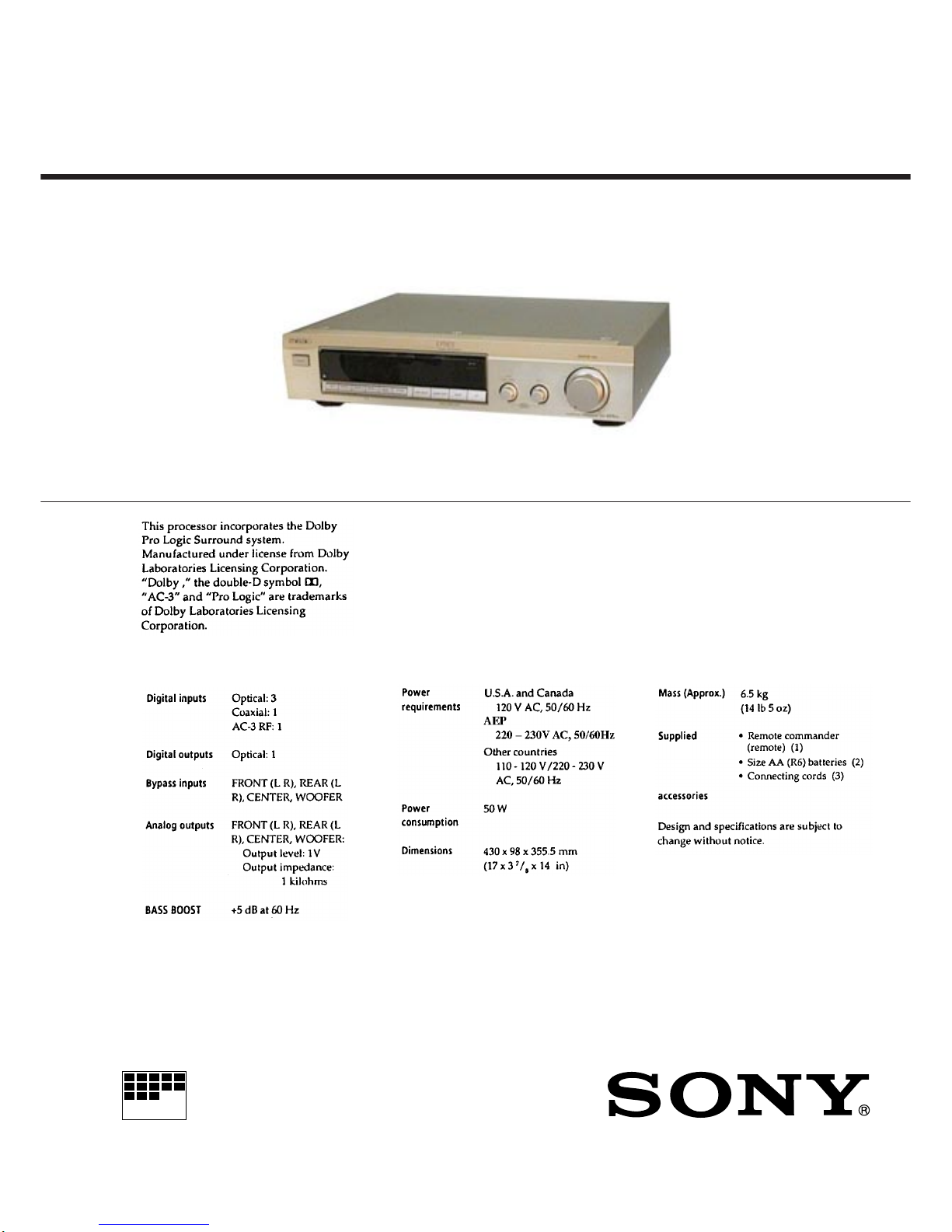
MODEL IDENTIFICATION
— BACK PANEL —
US model
CND model
AEP model
E, MY, SP, CH model
4-987-861-1
4-987-861-2
4-987-861-3
4-987-861-4
MODEL PARTS No.
ATTENTION AU COMPOSANT AYANT RAPPORT
À LA SÉCURITÉ!!
LESCOMPOSANTSIDENTIFIÉSPAR UNE MARQUE!SUR
LES DIAGRAMMES SCHÉMATIQUES ET LA LISTE DES
PIÈCES SONT CRITIQUES POUR LA SÉCURITÉ DE
FONCTIONNEMENT. NE REMPLACER CES COMPOSANTS
QUE PAR DES PIÈCES SONY DONT LES NUMÉROS
SONT DONNÉS DANS CE MANUEL OU DANS LES
SUPPLÉMENTS PUBLIÉS PAR SONY.
SAFETY-RELATED COMPONENT WARNING !!
COMPONENTS IDENTIFIED BY MARK !OR DOTTED LINE
WITH MARK !ON THE SCHEMATIC DIAGRAMS AND IN
THE PARTS LIST ARE CRITICAL TO SAFE OPERATION.
REPLACE THESE COMPONENTS WITH SONY PARTS
WHOSE PART NUMBERS APPEAR AS SHOWN IN THIS
MANUAL OR IN SUPPLEMENTS PUBLISHED BY SONY.
TABLE OF CONTENTS
1. SERVICING NOTE ........................................................... 3
2. GENERAL ............................................................................ 4
3.TEST MODE ...................................................................... 12
4. ELECTRICAL ADJUSTMENTS ................................ 15
5. DIAGRAMS
5-1. Circuit Boards Location .................................................... 16
5-2. Block Diagrams
• D/A Section .................................................................... 17
• AC-3 (RF) Section ......................................................... 19
• Control Section............................................................... 21
• Power Section................................................................. 23
5-3. Printed Wiring Board — Main Section — ........................ 25
5-4. Schematic Diagram — Control Section — ....................... 29
5-5. Schematic Diagram — Dolby AC-3 Section —................ 32
5-6. Schematic Diagram — D/A Section —............................. 35
5-7. Printed Wiring Board — Display Section — .................... 39
5-8. Schematic Diagram — Display Section — ....................... 43
5-9. Printed Wiring Board — Power Section — ...................... 46
5-10. Schematic Diagram — Power Section — ......................... 49
5-11. IC Pin Functions
• IC201 System Controller (HD6433397A13F) ............... 51
• IC301 Digital Audio Interface Receiver (LC8905V)..... 53
• IC401, 402, 403 Sampling Rate Converter
(CXD8517Q) .................................................................. 54
• IC423 Digital Signal Processor (SSP424923)................ 55
• IC424 Digital Signal Processor (DSP56009) ................. 57
• IC901 Digital Signal Processor (AC-3 RF Demodulator)
(PD4606A) ..................................................................... 59
5-12. IC Block Diagrams ............................................................ 62
6. EXPLODED VIEWS
6-1. Front Panel Section............................................................ 67
6-2. Chassis Section .................................................................. 68
7. ELECTRICAL PARTS LIST ......................................... 69
• Abbreviation
CND : Canadian model.
MY : Malaysia model.
SP : Singapore model.
CH : Chinese model.
Notes on chip component replacement
• Never reuse a disconnected chip component.
• Notice that the minus side of a tantalum capacitor may be
damaged by heat.

— 3 —
SAFETY CHECK-OUT
After correcting the original service problem, perform the following
safety checks before releasing the set to the customer:
Check the antenna terminals, metal trim, “metallized” knobs, screws,
and all other exposed metal parts for AC leakage. Check leakage as
described below.
LEAKAGE
The AC leakage from any exposed metal part to earth Ground and
from all exposed metal parts to any exposed metal part having a re-
turn to chassis, must not exceed 0.5 mA (500 microampers). Leak-
age current can be measured by any one of three methods.
1. A commercial leakage tester, such as the Simpson 229 or RCA
WT-540A. Follow the manufacturers’ instructions to use these
instruments.
2. A battery-operatedACmilliammeter.The DataPrecision 245 digi-
tal multimeter is suitable for this job.
3. Measuring the voltage drop across a resistor by means of aVOM
or battery-operated AC voltmeter. The “limit” indication is 0.75
V, so analog meters must have an accurate low-voltage scale.The
Simpson250and SanwaSH-63Trd are examplesof a passiveVOM
that is suitable. Nearly all battery operated digital multimeters that
have a 2V AC range are suitable. (See Fig. A)
Fig. A. Using an AC voltmeter to check AC leakage.
To Exposed Metal
Parts on Set
0.15
µ
F1.5k
Ω
AC
voltmeter
(0.75V)
Earth Ground
SECTION 1
SERVICING NOTE
RV901 of Main Board
RV901 of the main board requires no adjustments. Please note that it
should be dixed to mechanical center position when you moved and
do not know origin position.
Connection andTest Disc
Connection of this unit to a AC-3 Dolby surround equipment will
realize outstanding sound playback.
Check if the respective surround channel outputs are playing back
normally by the following method.
Jig :
Discription Part No.
AC-3 TEST LD J-2501-132-A
Connected Equipment:
AC-3 LD player
(This unit is also compatible with the digital versatile disc player
(DVD). The DVD must be checked with the LD player using all
the circuits of this unit.)
Connecting Method:
AC-3 compatible
LD player
AC-3 RF output terminal Coaxial digital
connectingcableVMC-10G,etc.(Optional)
Unit
AC-3 RF
output terminal AC-3 RF
input terminal
Checking Method:
Play back a test disc of the LD player, and check if the contents
recorded on the disc case (printed on the disc case) are played
back normally.

— 4 —
SECTION 2
GENERAL This section is extracted from
instruction manual.

— 5 —

— 6 —

— 7 —

— 8 —

— 9 —

— 10 —

— 11 —

— 12 —
SECTION 3
TEST MODE
Self-Diagnosis andTest Mode
This unit is provided with a “self-diagnosis and self-recovery func-
tion” which detects DSP errors and automatically recovers the unit,
and a test mode for performing operation checks during repairs.
1. Main Functions
• DSP self-diagnosis and self-recovery function
• Self-diagnosis for servicing and error message display
• Display of history of past DSP errors
• Various operation check mode
• SRAM, EEPROM check function
• Initialization (Differs according to country)
VOLUME LED
2. Entering theTest Mode
1. While pressing the AC-3 RF button and DIGITAL 2 button
simultaneously in the power OFF state, press the POWER but-
ton.
2. When the VOLUME LED starts blinking, release these buttons.
The self-diagnosis for servicing will be executed, and the opera-
tion check mode will be set.
(NOTE: Performing initialization will erase the error history. Do
not therefore press the wrong buttons. For details, refer to “5. Ini-
tialization” on page 14.)
3. Self-diagnosis Mode for Servicing/Display of
History of DSP Errors
3-1. Self-diagnosis Mode for Servicing
Before entering the test mode, first the following self-diagnosis pro-
gram for servicing will be run.
1. Checks if unintended buttons are being pressed
2. Checks EEPROM (External memory device) operation
3. Read/write test of DSP external memory (1M SRAM)
4. Checks and displays history of various DSP abnormal operations
• When an error is detected:
The error message is displayed for about 8 seconds on the fluores-
cent display tube, it is switched to “DOLBY SURROUND”, and
the operation check mode is set. (See Table 1.)
When several errors occur at the same time, only the first error
detected will be displayed.
• When no error is detected:
“softwareversion X. XX” will be displayed,andthe operation check
mode will be set. (X. XX means its version No.)
Table-1:
Error Message/Fluo-
rescent Display Tube Possible Reasons
VOLUME LED blinks
and fluorescent display
tube is OFF*
An unintended button is pressed, or connection
faultof flexible board between MAIN board and
DISPLAY board.
EEPROM read error!
EEPROM write error!
S-RAM access error!
DSP error detected!
Soldering fault or malfunction between IC202
(MAIN board AT24C02) and IC201 (MAIN
board microprocessor).
Reached end of IC202 (MAIN boardAT24C02)
writing life or incorrect insertion of part.
*NOTE:
Refer to “6. Check of Pressing of Unintended Button” on page 14.
Soldering fault between IC422 (MAIN part 1M
SRAM) and IC423 (MAIN board SSP424023)
When a DSP error is detected
(Refer to “3-2. Display of History of Abnormal
DSP Operations”.)

— 13 —
3-2. Display of History of DSP Operations
• When “DSP error detected!” is displayed on the fluorescent dis-
play tube, the history of DSP errors will be displayed eight seconds
later. (See Fig. 1.)
• This history will be displayed if a DSP error has occurred in the
past. It helps the detection of malfunction parts by enabling past
problems of the unit to be checked.
• This history shows the “Cause of error” and “How many times
occurred” for the two DSPs. (See Fig. 1.)
Fig. 1
Corresponding DSP
Contents of fluores-
cent display tube
: 1st DSP (DSP56009) 2nd DSP (SSP424023)
: 123x0000 123x0000
↑↑
4
↑
3
↑
2
↑
1↑
4
↑
3
↑
2
↑
1
:
How to read the
display
4. Operation Check Mode
• During the operation check mode, functions can be set by pressing
the corresponding button. (See Table-3.)
• Each time a button is pressed, the corresponding function will be
displayed for about 8 seconds.
• Buttons other than those displayed in Table-3 operate usually.
NOTE: Do not press the SET UP button during the operation check
mode.As this button is provided with a special function for
debugging, pressing it may impede the normal output of
signals in the sub-woofer mode.
Table-3:
Button Function
Outputs the Lch DIGITAL-2 input signal to
theREAR Lch and the Rch to theREAR Rch.
Fluorescent
Display Tube
Display
Outputs the Lch DIGITAL-3 input signal to
the CENTER and the Rch only to the
WOOFER.
Outputs the Lch DIGITAL-4 input signal to
the FRONT Lch, REAR Lch, CENTER, and
the Rch to the FRONT Rch, REAR Rch, and
CENTER.
DIGITAL2
DIGITAL3
DIGITAL4
OFF
DIG-2
(L-SL, R-SR)
DIG-3
(L-C, R-SW)
DIG-4
(L, R-ALL)
Whole fluorescent display tube lit check
Each time the button is pressed, the fluorescent display tube
lights up as follows.
Lit totallynLit partially 1nLit partially 2nLit totally....
By pressing the MENU knob and displaying “<<< LEVEL ADJUST >>>”,
and rotating the +/– knob to the right, the input signal selected at that time
can be output to any Lch or Rch channel.
(See Table-4.)
Table-4:
Fluorescent Display
Tube Display Output Destination of Input Signal
Outputs the FRONT Lch/Rch signal only to the
REAR Lch/Rch.
Outputs the FRONT Lch signal only to the
REAR Lch, and FRONT Rch signal to the
REAR Rch.
Outputs the FRONT Lch/Rch signal to the
FRONT Lch/Rch, the REAR Lch/Rch signal to
the REAR Lch/Rch, the CENTER signal to
CENTER, and the WOOFER signal to
WOOFER as usual.
Outputs the FRONT Lch signal to the FRONT
Lch, REAR Lch, and CENTER, and the
FRONT Rch signal to the FRONT Rch, the
REAR Rch, WOOFER.
Exchange(L-SL, R=SR)
Exchange (L-C, R=SW)
Exchange (NORMAL)
Exchange (L, R-ALL)
Number of times the error has occurred
↑
How to read the display
• The left side shows the errors of the first DSP (DSP56009:MAIN
board IC424) and the right side shows the errors of the second DSP
(SSP424023:MAIN board IC423).
• The “How many times occurred” indicates the number of times
that the error has occurred. If an error has occurred more than 256
times, it will be displayed as 256.
• The 1234part shows 0 or 1 according to the cause of the
error. If an error has occurred, 1 will be displayed. If no error has
occurred, 0 will be displayed. (See Table-2.)
Table-2:
Cause of error Possible cause
Mostly due to faulty connection (soldering) be-
tween DSP and microprocessor
Faulty DSP clock (X401 and onwards), faulty
DSP part, etc.
Overrunning of DSP due to heat, microprocessor
bugging, or IC301 (MAIN board PLL) is faulty
Faulty DSP part, or faulty microprocessor part,
etc.
1Failed in initial
booting
2DSP does not
operate
3Communication
port malfunction
4No reply from DSP
NOTE: This history is memorized in the EEPROM until the unit is
initialized. (Refer to “5. Initialization” on page 14.)

— 14 —
5. Initialization (Differs according to destination)
After executing the test mode, be sure to perform initialization.
• AEP, E, MY, SP, CH models
While pressing the AC-3 RF button and DIGITAL3 buttons
simultaneously, press the POWER button. When the VOLUME
LED starts blinking, release the buttons. “initialized (J/SP/CE)”
will be displayed on the fluorescent display tube, and all internal
settings will be returned to the initial values.
• US, CND models
While pressing the AC-3 RF button and DIGITAL4 buttons
simultaneously, press the POWER button. When the VOLUME
LED starts blinking, release the buttons. “initialized (U/CA)” will
be displayed on the fluorescent display tube, and all internal set-
tings will be returned to the initial values.
NOTE: As all histories of abnormal DSP operations will be erased,
note down the contents of the history beforehand.
6. Check of Pressing of Unintended Button
• This check is always performed when the power is turned ON.
Therefore when an error occurs, it can be known without setting
the test mode because the VOLUME LED blinks and the fluores-
cent display tube stops displaying.
• When an unintended button is pressed during the test mode or ini-
tialization, theVOLUME LED also blinks, and the fluorescent dis-
play tube stops displaying, preventing no mode to be set.
7. Other Functions
In the personal use of the unit at home, if no sounds are produced due
to DSP problems, the DSP will be rebooted automatically to attempt
recovery. If no sounds are still produced after five retries, “Turn
POWER SW off!” will be displayed on the fluorescent display tube.
If this problem occurs, it indicates that the DSP is faulty or the user’s
setting environment may be unsuitable. Refer to “3. Self-Diagnosis
Mode for Servicing/Display of History of DSP Errors” on page 12 to
identify the problems.
• Abbreviation
CND : Canadian model
MY : Malaysia model
SP : Singapore model
CH : Chinese model

— 15 —
SECTION 4
ELECTRICAL ADJUSTMENTS
PLL Free-running Adjustment
Connection :
Frequency counter
Adjusting Method :
1. Connect the frequency counter to TP (LRCK).
2. Turn On the power switch.
3. Adjust RV301 of the main board so that the frequency of TP
(LRCK) becomes the specified value.
Specified value: 44.5 kHz ± 0.5 kHz
Adjusting point: Main Board
RV901 of Main Board
RV901 of the main board requires no adjustments. Please note that it
should be dixed to mechanical center position when you moved and
do not know origin position.
Adjustment Location :
[ MAIN BOARD ] — SIDE A —
RV301
Free-running
TP
(LRCK)
Main board
TP (LRCK)
RV901
No Adjustment

— 16 —
SECTION 5
DIAGRAMS
5-1. CIRCUIT BOARDS LOCATION
AC2 board
SW board
PS board
DISPLAY board
VOL board
MAIN board
TR board
AC1 board

— 18 —— 17 —
5-2. BLOCK DIAGRAMS
—DA SECTION—
SDP-EP9ES
3OUT
DIGITAL
INPUT
IC306
5
DIGITAL 1
3OUT
DIGITAL
INPUT
IC305
DIGITAL 2
4
3OUT
DIGITAL
INPUT
IC304
DIGITAL 3
3
DAO 6
SELECTOR
IC302
7
D1
D2
D3
D0
14 2
A0 A1
Y
DSELA0
DSELA1
D
CONTROL
SECTION
C
DOLBY
AC-3
SECTION
32
INPUT 4 BUFFER
IC307
14
15
16
17
24
10
DIRCLK
DIRLAT
DIWDAT
DIRDAT
DIRERR
DIRRST
E
CONTROL
SECTION
2
1
23
3
DIGITAL AUDIO
INTERFACE RECEIVER
IC301
DIN2
DIN1
DATAO
E/D OUT
10
1
DIGITAL
OUTPUT
IC303
VIN
B2 Y2
SELECTOR
IC404
(1/2)
9
A
DATA
CONTROL
SECTION
REC OUT
OUTPUT
B
CONTROL
SECTION
1
2
3
DATAI
LRCKI
BCKI
SAMPLING
RATE
CONVERTER
SAMPLING
RATE
COUNTER
7FI128
DATAO
LRCKO
BCKO
13
10
INIT
XI
SAMPLING RATE
CONVERTER
IC401
25
24
27
28
IN1+
IN1-
IN2+
IN2-
ECL
SW
VOLUME
CONTROL
IO1-
IO2+
IO2-
IO1+
4
5
2
1
DIGITAL VOLUME
IC410
VCNT
+
+
L.P.F.
L.P.F.
IC416 IC602
MIX
AMP H.P.F. BUFFER
IC607
12
15
D/A
CONVERTER
SHIFT
REGISTER
LEVEL
SHIFT
CK
2
1 3
DT
ST
D/A
CONVERTER
IC421
1
IC425
13
12
8
9
2
1
FILTER
F401
X401
49.152MHz
FILTER
F402
12
7
4
5
2
1
3
6
13
11
22
21
20
1
2
3
DATAI SAMPLING
RATE
CONVERTER
DATAO
SAMPLING
RATE
COUNTER
FLAME
COUNTER
7
10
INIT
13
XI
SAMPLING RATE
CONVERTER
IC403
DATAI
LRCKI
BCKI DIGITAL
FILTER D/A
CONVERTER
R1(+)
R1(-)
R2(+)
R2(-)
21
23
18
16
MODE
CLOCK
GENERATOR
10
DIGITAL FILTER, D/A CONVERTER
IC405
FILTER
F404
DATAI
LRCKI
BCKI DIGITAL
FILTER D/A
CONVERTER
R1(+)
R1(-)
R2(+)
R2(-)
21
23
18
16
MODE
CLOCK
GENERATOR
DIGITAL FILTER, D/A CONVERTER
IC407
10
REAR
L-CH
ANADIG
EXTAL
SRCINI
DF-DAT
DF-CLK
DF-LAT
DF-INI
ATT
SHIFT
LATCH
INIT
DA-LAT
DA-CLK
DA-DAT
ST
CK
DT
F. 8DB
R. 8DB
C/S.8DB
F. 4DB
R. 4DB
C/S. 4DB
MUT
RY-OFF
F
CONTROL
SECTION
MUT
RY-OFF
3
RY607
5
4
1
3
RY608
5
4
1
F
J601
FRONT
L
RY609
1
RY610
1
R
J601
REAR
L
8
76
7
86
REAR L-CH
R.8DB
R.4DB
RY611
1
RY612
1
C
J602
CENTER
7
86
7
86
CENTER
C/S.8DB
C/S.4DB
MUT
RY-OFF
MUT
RY-OFF
F
R
C
FRONT
L
REAR
L
CENTER
BYPASS
J603
OUT
PUT
F.8DB
F.4DB
AVOCK
LRCK
BCK
FS128
SCLK
XLAT
SWDT
SRDT
EROR
XMODE
SELECTOR
IC404 (2/2)
Y0
Y1
Y2
B0
B1
B3
SA0A1
BCK
LRCK
128FS
IC408 1
213
12
3
4
10 11
65
9
8
30
32
31
LRCKO
BCKO
40
39
38
45
34 35 36 37
SHIFT
LATCH
INIT
ATT
XIN
512FSO
45 512FSO
34 35 36 37
XIN
SHIFT
LATCH
INIT
ATT
30
32
31
40
39
38
FLAME
COUNTER
INPUT
J301
BCKO
LRCKO
SOA
SOB
SOC
CENTER
SUPER WOOFER
BUFFER
LRCKI
BCKI
FI128
R-CH, SUPER WOOFER is omitted.
REAR L-CH and CENTER part was omitted.
(Same as FRONT L-CH)
Signal path
:Digital in
:Digital out
:RF (AC-3)
•
•
•
09
6RV301
PLL
(Page 22)
(Page 21)
(Page 20)
(Page 21)
(Page 21)
(Page 22)
VIN

— 20 —— 19 —
—AC-3 (RF) SECTION—
SDP-EP9ES
AC-3
RF
INPUT BUFFER
Q902
J901 3L.P.F.
IC902 1BUFFER
Q903 1
46
9
FILTER
FL902
BUFFER
Q904
+
27
COMPARATOR
IC903
COMPARATOR
5
6
7
RV901
NO ADJUSTMENT
AMP
IC904
IC904
31
DIN DEMODULATION S/P ERROR
CORRECTOR DAI
CONTROL
DIVIDER
DIGITAL
OUT DAO
65
DAOUT
DIGITAL
PLL
4
X902
46.08MHz
L.P.F.
IC905 PHASE
COMPARATOR
DIVIDER
V1
41
X901
18.432MHz INVERTER
IC906
55
57
78
X LOCK
MUTE SW
Q901
51 - 43
DB0 - DB8 21 - 24•26•27•30•31•37•38•42•39•33•34
A0 A14
ADDRESS
GENERATOR
27 22
S RAM
IC907
WE
OE
DB0 - 4
A0 - 14
27 22
WE
OE
11 - 13•15 - 19
I/O0 I/O7 11 - 13•15 - 19
I/O0 I/O7
10 - 3•25•24•21•23•2•26•1
A0 A14 10 - 3•25•24•21•23•2•26•1
A0 A14
S RAM
IC908
DB5 - 8
DB0 - 8
WE
OE
A0 - 14
A0 - 14
DATA - BUS DB0 - DB8
35 41
ADDRESS - BUS A0 - A14
INTERFACE 8 AC. RST
RESET
59
MUTO MUTO
G
CONTROL
SECTION
C
D/A
SECTION
82
XIN
PDO
98
IC906
13 10
IC906
+
-
IC902
67
MUTI
09
DIGITAL SIGNAL PROCESSOR
(AC-3 RF DEMODULATOR)
IC901
• Signal path
:RF (AC-3)
(Page 17)
(Page 21)
CPU

—CONTROL SECTION—
SDP-EP9ES
SDO0
SDO2
SDO1
AUDIO
I/F
SDI0
SDI1
27 26
DIGITAL SIGNAL
PROCESSOR
HOST
I/F
MEMORY
PLL
SCKR
WSR
35 41 42 43 36
EXTAL
SCK
MISO
MOSI
SS
HREQ
RESET
SDO0
SDO1
AUDIO
I/F
SDI0
SDI1
27 26
BCKO
LRCKO
DATA
DIGITAL SIGNAL
PROCESSOR
HOST
I/F
MEMORY
PLL
57
•
56
51
55
SCKR
WSR SCKT
WST
47
•
46
35 41 42 43 36
EXTAL
SCK
MISO
MOSI
SS
HREQ
RESET
MEMORY
I/F
24 29 13 - 15•17 - 21
71•69 - 67•65 - 62 25 - 22•20 - 18•16•14 - 11•7•5 - 3
12 - 5•26•27•23•25•4•28•3•2
S RAM
IC422
15 16
56
SCL
SDA
EEP ROM
IC202
262728
1
17
68
69
70
71
72
74
75
77
76
80
2•3
1
OUT
X201
16MHz SIRCS
RECEIVER
IC256
18 19 22 - 20
511 - 9
YA0 - A2
SELECT SWITCH
IC254,255
4 - 1•15 - 12
D0 D7
KEY ARRY
ROTARY
ENCODER
10139
11
29 5 430
3
26 - 17•16 - 7
FLUORESCENT INDICATOR TUBE
FL251
29
24 26
1 - 20•41 - 56
25 23 24
3
27
8
M
DRIVER
RV251
CONTROL
SWITCH
Q601 - 616
+8DB SWITCH
Q617, 618, 621,
622,625,626
+4DB SWITCH
Q619, 620, 623,
624,627,628
MD0 MD7 DA0 MA15
SOA
SOB
SOC
B
D/A
SECTION
EXTAL
ANADIG
SRCINI
DF-DAT
DF-CLK
DF-LAT
DF-INI
DA-LAT
DA-CLK
DA-DAT
F. 8DB
R. 8DB
C/S. 8DB
F. 4DB
R. 4DB
C/S. 4DB
MUT
RY-OFF
ANADIG
SRCINI
DF-DAT
DF-CLK
DF-LAT
DF-INI
DA-LAT
DA-CLK
DA-DAT
50
51
52
53
54
55
57
58
59
F
D/A
SECTION
MASTER VOL
LED DRIVE
Q251
VOLUME MOTOR DRIVE
IC253
34 37 35
CK
CL
(NC)
STB
(NC)
DI
OUT1
OUT36
FFROM
POWER TRANSFORMER
DOUT
DIN
CLK
CL
LS
OUT0
OUT20
FL-DAT
FL-CLK
FL-CLR
FL-LAT
DISPA0
DISPA2
FL DRIVER
IC251, 252
DISPD0
DISPD1
SIRCSI
XTAL
•
EXTAL
STOP
RESET
RF-ERR
REF-RES
DSELA0
DSELA1
DIRERR
DIRCLK
DIRLAT
DIWDAT
DIRDAT
DIRERR
DIRCLK
DIRLAT
DIWDAT
DIRDAT
DSELA0
DSELA1
DIRRST
STOP
RESET
MUTO
AC. RST
G
DOLBY
AC-3
SECTION
POWER
SECTION
D
D/A
SECTION
E
D/A
SECTION
A
D/A
SECTION
41 40 39
M9SCLK
MISO
M9MOSI
M9MOSS
M9MORQ
M9MRES
ROMCLK
ROMDAT
48 46 44 43 42 45 31
M4SCLK
M4MISO
M4MOSI
M4MOSS
M4MORQ
M4MRES
AN1
62
64
66
63
65
67
61
60
LR+8DB
SS+8DB
CS+8DB
LR+4DB
SS+4DB
CS+4DB
MUT
RY-OFF
30
VOLLED
AN0
VOLUME+
VOLUME-
SYSTEM CONTROL
IC201
76
GPIO0
77 78 80
MRD
MWR
57
•
56
51
55
49
50
SCKT
WST
47
45
46
31
CE
R/W
A16
D0 D7 A0 A15
DIGITAL SIGNAL PROCESSOR
IC424 DIGITAL SIGNAL PROCESSOR
IC423
49
50
MCAS
H
• Signal path
:Digital in
09
(Page 17)
(Page 17)
(Page 17)
(Page 20)
(Page 23)
(Page 17)
(Page 17)
— 21 — — 22 —

— 23 —
— POWER SECTION —
SDP-EP9ES
F
TO FLUORESCENT
INDICATOR TUBE
T1
POWER TRANSFROMER
RECT
D115, 116
FL. +30V
STOP
+5V REG
Q103,104
+5V
D111
-13V
+30V REG
Q106
+5V REG
Q251,254
FLD. +5V
RECT
D113, 114
POWER - ON
DET
Q105
+
31
REG
CONTROL
IC102
3 2
RECT
D112
-5V REG
IC103
+13V
+15V REG
Q101
REG CONTROL
IC101,Q107
D110
2313
+5V REG
IC426
+7V REG
IC151
+15V
+B
+5V
REF
+7V
D104
D107
REG CONTROL
IC101,Q108
13
-7V REG
IC152
-7V
-15V
H
CONTROL
SECTION
-5V
-15V REG
IC102
AC
IN
POWER
S1
RECT
D101
13
RST
RESET
IC203
09
VOLTAGE
SELECTOR
S4
E,Malaysia,Singapore,
Chinese
(Page 21)
Other manuals for SDP-EP9ES
1
Table of contents
Other Sony Processor manuals