Sony ICD-CX50 - Visual Voice Recorder User manual

SERVICE MANUAL
Sony Corporation
Connect Company
Published by Sony Engineering Corporation
US Model
Canadian Model
AEP Model
UK Model
E Model
Tourist Model
VISUAL IC RECORDER
9-879-671-02
2005F04-1
© 2005.06
Ver. 1.1 2005.06
SPECIFICATIONS
ICD-CX50
IC recorder
Recording media Built-in flash memory 256 MB, Stereo/
Monaural recording
Recording time • ST: Approx. 11 hours 30 minutes
• STLP: Approx. 22 hours 5 minutes
• SP: Approx. 35 hours
• LP: Approx. 93 hours 30 minutes
Frequency range • ST: 60 Hz - 13,500 Hz
• STLP: 60 Hz - 7,000 Hz
•SP: 60 Hz - 7,000 Hz
• LP: 80 Hz - 3,500 Hz
Playback speed control (DPC)
+100% to -50%
Camera
Image file format JPEG
Number of pixels 1 280 ×960 pixels (approx. 1 340 000 pixels)
Picture size 1 280 960 pixels
640 ×480 pixels
Image device 5.00 mm (1/3.6 type) color CCD primary color
filter
Total pixels number of camera
1 360 ×986 pixels (approx. 1 340 000 pixels)
Effective pixels number of camera
1 308 ×976 pixels (approx. 1 280 000 pixels)
Lens Focal length f=4.3mm, horizontal angle of view
49.5 degrees
F-stop 4
Recommended camera distance
30 cm to infinite (Macro: 12 cm)
General
Speaker approx. 2.3 cm (29/32 in.) dia.
LCD panel used 1.2 inch D-TFD liquid panel, RGB, 64 levels of
gradations, 262 144 colors
Input/Output • Microphone jack (minijack, stereo)
– input for plug in power
• Headphones jack (minijack, stereo)
– output for 8 - 300 ohms headphones
• USB connector
• DC IN 6V jack
Power requirements 6 V DC, 800mA, rechargeable lithium-ion battery
Operating temperature
For recording/playback:
–10 °C to +45 °C (14 °F to 104 °F)
For charging:
+5 °C to +35 °C (41 °F to 95 °F)
Dimensions (w/h/d) (not including projecting parts and controls)
45.8 ×101.2 ×23.5 mm (1 13/16 ×4 ×15/16 in.)
Mass (including batteries)
99 g (3.5 oz)
Supplied accessories AC power adaptor AC-ES608K (1)
Plug adaptor (1) (supplied only in some regions)
Operating instructions (For the Visual IC
Recorder (1)/For the application software (1))
Stereo headphones (1)
USB connecting cable (1)
Application Software (CD-ROM) (1)
Carrying pouch (1)
Your dealer may not handle some of the above listed
optional accessories. Please ask the dealer for detailed
information.
Design and specifications are subject to change without
notice.

2
ICD-CX50
TABLE OF CONTENTS
1. GENERAL ................................................................... 3
2. DISASSEMBLY
2-1. Case (Front) ..................................................................... 4
2-2. Ornamental Belt Block Assy ........................................... 5
2-3. Case (U) Block Assy ....................................................... 5
2-4. Main Block Assy ............................................................. 6
2-5. MAIN Board, SWITCH Board ....................................... 6
2-6. JACK Board..................................................................... 7
2-7. Cover (U), Cover (Lcd) ................................................... 7
2-8. Camera Block Assy ......................................................... 8
2-9. LCD Board, LCD Unit ................................................... 8
3. TEST MODE ............................................................... 9
4. DIAGRAMS
4-1. Block Diagram – MAIN Section-1 – ............................. 12
4-2. Block Diagram – MAIN Section-2 – ............................. 13
4-3. Block Diagram – POWER Section –.............................. 14
4-4. Printed Wiring Board – MAIN Board – ......................... 15
4-5. Schematic Diagram – MAIN Board (1/6) – ................... 16
4-6. Schematic Diagram – MAIN Board (2/6) – ................... 17
4-7. Schematic Diagram – MAIN Board (3/6) – ................... 18
4-8. Schematic Diagram – MAIN Board (4/6) – ................... 19
4-9. Schematic Diagram – MAIN Board (5/6) – ................... 20
4-10. Schematic Diagram – MAIN Board (6/6) – ................... 21
4-11. Printed Wiring Board – CAMERA FLEXIBLE Board – 22
4-12. Schematic Diagram – CAMERA FLEXIBLE Board –.. 23
4-13. Printed Wiring Board – LCD Board – ............................ 24
4-14. Schematic Diagram – LCD Board –............................... 25
4-15. Printed Wiring Board – SWITCH FLEXIBLE Board –. 26
4-16. Schematic Diagram – SWITCH FLEXIBLE Board – ... 27
4-17. Printed Wiring Board – SWITCH Board – .................... 28
4-18. Schematic Diagram – SWITCH Section – ..................... 29
4-19. Printed Wiring Boards – JACK Section – ...................... 30
4-20. Schematic Diagram – JACK Section –........................... 31
5. EXPLODEDVIEWS
5-1. Case (Front) Section ........................................................ 35
5-2. Case (Rear) Section ......................................................... 36
5-3. Slider Section .................................................................. 37
5-4. Camera Section................................................................ 38
5-5. MAIN Board Section....................................................... 39
6. ELECTRICAL PARTS LIST .................................. 40
Flexible Circuit Board Repairing
•Keep the temperature of the soldering iron around 270 °C
during repairing.
•Do not touch the soldering iron on the same conductor of the
circuit board (within 3 times).
•Be careful not to apply force on the conductor when soldering
or unsoldering.
Notes on chip component replacement
•Never reuse a disconnected chip component.
•Notice that the minus side of a tantalum capacitor may be
damaged by heat.
✩Replacement of IC1001 used in this set requires a special tool.
•The voltage and waveform of CSP (chip size package) cannot
be measured, because its lead layout is different from that of
conventional IC.
•Lead layouts surface
Lead layout of
conventional IC CSP (chip size package)
UNLEADED SOLDER
Boards requiring use of unleaded solder are printed with the lead-
free mark (LF) indicating the solder contains no lead.
(Caution: Some printed circuit boards may not come printed with
the lead free mark due to their particular size)
: LEAD FREE MARK
Unleaded solder has the following characteristics.
•Unleaded solder melts at a temperature about 40 °C higher
than ordinary solder.
Ordinary soldering irons can be used but the iron tip has to be
applied to the solder joint for a slightly longer time.
Soldering irons using a temperature regulator should be set to
about 350 °C.
Caution: The printed pattern (copper foil) may peel away if
the heated tip is applied for too long, so be careful!
•Strong viscosity
Unleaded solder is more viscou-s (sticky, less prone to flow)
than ordinary solder so use caution not to let solder bridges
occur such as on IC pins, etc.
•Usable with ordinary solder
It is best to use only unleaded solder but unleaded solder may
also be added to ordinary solder. Operating instructiondd
SAFETY-RELATED COMPONENT WARNING!!
COMPONENTS IDENTIFIED BY MARK 0OR DOTTED LINE
WITH MARK 0ON THE SCHEMATIC DIAGRAMS AND IN
THE PARTS LIST ARE CRITICAL TO SAFE OPERATION.
REPLACE THESE COMPONENTS WITH SONY PARTS WHOSE
PART NUMBERS APPEAR AS SHOWN IN THIS MANUAL OR
IN SUPPLEMENTS PUBLISHED BY SONY.
ATTENTION AU COMPOSANT AYANT RAPPORT
À LA SÉCURITÉ!
LES COMPOSANTS IDENTIFIÉS PAR UNE MARQUE 0SUR
LES DIAGRAMMES SCHÉMATIQUES ET LA LISTE DES
PIÈCES SONT CRITIQUES POUR LA SÉCURITÉ DE
FONCTIONNEMENT. NE REMPLACER CES COM- POSANTS
QUE PAR DES PIÈCES SONY DONT LES NUMÉROS SONT
DONNÉS DANS CE MANUEL OU DANS LES SUPPLÉMENTS
PUBLIÉS PAR SONY.

3
ICD-CX50
SECTION 1
GENERAL This section is extracted
from instruction manual.
Index to Parts and Controls
Identifying the front and rear panels of the unit
1Lens mount (HOLD on/off, Camera on/off,
camera self mode)
You can set the unit to the following modes as you
rotate the lens mount to the following position:
HOLD on: When you rotate the lens mount to
“HOLD”, “HOLD”will appear for 3 seconds and
then the display will be turned off.
• During recording and playback: recording or
playback continues but the functions of the
buttons are locked.The live view mode, if
activated, will be turned off.
• During stop: The unit enters into the standby
mode.
To cancel the HOLD function
Rotate the lens mount to select other position.
zHOLD off/Camera off: When you rotate the lens
mount to the “z” position, you can record a
message but cannot shoot an image.If the lens
mount is turned from the HOLD position, HOLD
will be canceled.
Camera on (Open): Rotate the lens mount further
than “zHOLD off/Camera off” position and to
the next position it clicks into place.This position
is called “Camera on (Open)”position in this
manual where the camera is activated.You can
turn on the live view mode.
Camera on (Self): Rotate the lens mount further
than “Camera on (Open)”position until it clicks
into place.The lens faces towards you.This
position is called “Camera on (Self)”positionYou
can turn on the live view and can shoot your self
view.
2Macro switch (off/ on)
You can turn on or off the macro feature when you
shoot an image in the live-view mode.
on:Turns on the macro feature for shooting close-
ups.
off:Turns off the macro feature.
3
Display cover
When the LCD cover is open:You can view the LCD
display in full-screen. You can also activate the
live view mode to shoot an image.
When the LCD cover is close: You cannot activate
the live view mode or display the menu.
4Display window (with built-in speaker)
For the details, see “Using the display window”
below.The built-in speaker outputs sound when no
headphones or active speaker are connected.
Note
When the display window is contaminated, use the
inner cloth of the carrying pouch supplied or a soft
cloth such as glasses cleaning cloth to wipe the
screen surface softly.
5CHG (Charge) lamp
Lights in red when the built-in battery is being
charged.
6REC (record)/PLAY indicator
The indicator lights in red during recording or in
green during playback. It flashes in red during
recording pause.During accessing the data, it flashes
in red or orange.
7CAPTURE button
Press to shoot an image.If the live view is not
activated, pressing this button activates the live view
mode.
8REC (record) /PAUSE button
Press here to start and pause recording.
9(camera) button
Turns on or off the live view mode for shooting an
image.
0Built-in stereo microphone
qa DISPLAY/MENU button
By pressing briefly, it works as DISPLAY button to
change the display as follows:
In the live view mode:Turns off and on the display
of image information.
When the live view is off: Switches the thumbnail
view of the messages or bookmarks and full-
screen preview of an image.
By pressing for more than one second, it works as
MENU button to display the menu on the LCD
display.
qs Control key
b/ B( : Folder/ : Message/ : Bookmark)/
v(.: fast backward•zoom out)/V(>: fast
forward•zoom in)/u (play/pause•enter)
qd x(stop) button
Press here to stop operation.
qf VOL (volume) +/– button
Adjust the playback sound volume with the button.
qg V-UP (DigitalVoice Up) ON/OFF switch
You can make the playback sound well-balanced and
more audible by enabling the Digital Voice Up
function as follows:
ON: Digital Voice Up function is activated. Inaudible
low-level part of a recorded message is amplified
so that the overall recording is adjusted to its
optimum level.
OFF: A message is played back without DigitalVoice
Up function.
Note
Depending on the area you purchased the unit, the
Digital Voice Up switch name shown on the unit may
differ.
qh RESET button
In case the unit cannot be operated, press here with a
pointed object for more than 0.5 second.
qj Slit for a handstrap
You can attach a handstrap (not supplied) here.
qk Camera lens
ql i(headphones) jack
To monitor the recording from the built-in
microphone, connect headphones supplied or not
supplied here.You can adjust the volume withVOL
+/– qf, but the recording level is fixed.
w; m(microphone) jack (PLUG IN POWER)
You can connect an external microphone here.When
an external microphone is connected, the built-in
microphone is automatically cut off.
wa DC IN 6V jack
Connect the supplied AC power adaptor for
charging.
ws USB connector
Use the supplied USB cable to connect the unit to a
PC.
Opening the display
cover.
4
ICD-CX50
Note: Follow the disassembly procedure in the numerical order given.
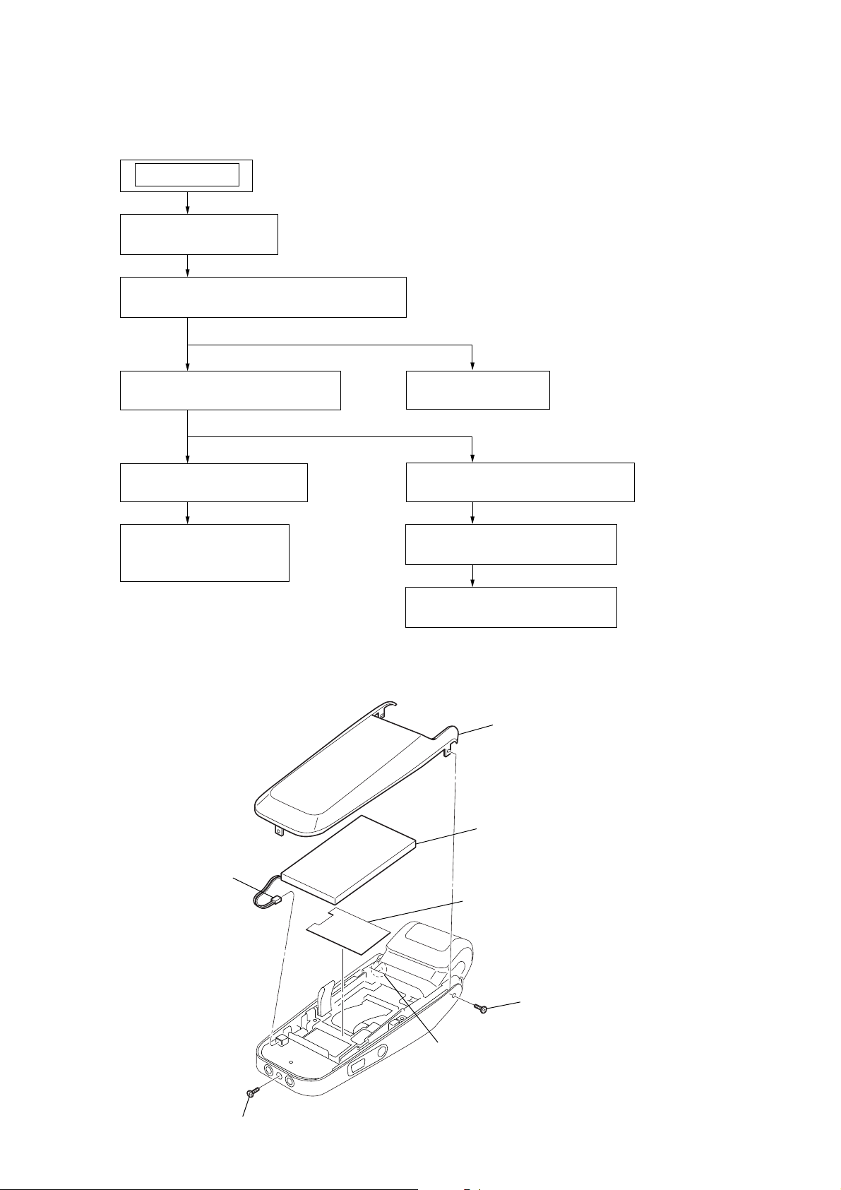
2-1. CASE (FRONT)
SECTION 2
DISASSEMBLY
1
ornament pin (minus
)
4
CN7502
3
case (front)
5
lithium ion storage battery
6
sheet (flexible)
claw
2
ornament pin (minus)
•This set can be disassembled in the order shown below.
2-1. CASE (FRONT)
(Page 4)
2-3. CASE (U) BLOCK ASSY
(Page 5) 2-6. JACK BOARD
(Page 7)
SET
2-5. MAIN BOARD,
SWITCH BOARD
(Page 6)
2-8. CAMERA BLOCK ASSY
(Page 8)
2-9. LCD BOARD, LCD UNIT
(Page 8)
2-2. ORNAMENTAL BELT BLOCK ASSY
(Page 5)
2-4. MAIN BLOCK ASSY
(Page 6) 2-7. COVER (U), COVER (LCD)
(Page 7)

5
ICD-CX50
2-2. ORNAMENTAL BELT BLOCK ASSY
2-3. CASE (U) BLOCK ASSY
1
precision pan screw
(M 1.4)
6
ornamentl belt block assy
7
MICROPHONE board
2
three precision pan screws
(M 1.4)
4
cap (USB)
3
precision screw
(+P 1.7
×
8)
5
two screws
(M 1.4)
1
CN20002
4
case (U) block assy
2
two screws
(M 1.4)
3
screw
(M 1.4)

6
ICD-CX50
2-4. MAIN BLOCK ASSY
2-5. MAIN BOARD, SWITCH BOARD
2
precision pan screw
(M 1.4)
6
SWITCH FLEXIBLE board
7
main block assy
3
precision pan screw
(M 1.4)
5
CN20103
4
1
two sheets (LED)
1
precision pan screw
(M 1.4)
4
two precision pan screws
(M 1.4)
2
SWITCH board
5
MAIN board
chassis (PWB)
3
CN21304

7
ICD-CX50
2-6. JACK BOARD
2-7. COVER (U), COVER (LCD)
2
JACK board
ornament belt section
1
precision pan screw
(M 1.4
×
3.5)
2
screw
(M 1.4)
3
screw
(M 1.4)
4
cover (LCD)
5
camera block section
1
cover (U)

8
ICD-CX50
2-8. CAMERA BLOCK ASSY
2-9. LCD BOARD, LCD UNIT
3
CN8601
5
holder (F)
4
case (U) assy
slider section
6
camera block assy
2
Rotate the camera block assy
two and quarter.
1
P2 tapping screw
(M 1.7 )
1
screw
(M 1.4)
2
screw
(M 1.4)
4
half rotation loosens the screw.
3
half rotation loosens the screw.
5
9
7
precision pan screw
(M 1.4)
BLK GRY
RED
slider assy
8
precision pan screw
(M 1.4)
0
LCD board
qa
LCD unit
6
Remove the three solders.

9
ICD-CX50
This set provides the checks given below in TEST MODE.
Setting theTEST MODE
Turn on power to the set. Press [V-UP] key while pressing bkey
and [Camera] button at the same time.
Exiting theTEST MODE
Press [RESET] switch.
TEST MODE Menu
The menu given below appears when TEST MODE is entered.
Select an item using >/ .key and determine the selected
item using ukey.
1.Version
Check the version of each module.
ICX-165 build:Language
(JP: Japanese, US: English, and CN: Chinese)
ARM : F/W version for CPU (ARM unit)
SHE : F/W version for SUB-CPU
DSP : F/W version for CPU (DSP unit)
IPL : F/W version for IPL
Date : Build date and time
2. Key Check
Check the input by pressing each key.
Input and INT check (KEY input acceptance check and
KEY_XWAKE interrupt check).
Target input keys:
[MACRO] / [CAM-DET] / [HOLD] / [DISPLAY/MENU] / u /
>/ ./ b/ B/ x/ [VOL +] / [VOL --] / [V-UP] /
[CAMERA] / [CAPTURE] / [REC/PAUSE] / [LCD COVER]
Total of 17 key locations
The backlight is lit for 0.5 sec. when a key input is accepted.
3. Language
Check the languages and change between them.
The default is Japanese.
Example of LCD display
4. Loop Back
Perform a DSP LOOP BACK.
5. Beep
Sound 1.3kHz beep.
6. System
Perform three types of self tests: NOR, NAND and PORT.
OK is displayed if normal operation is confirmed by the test.
7. Battery
Check the current value of BatteryA/D.
8. DC-IN
Check the current value of DC-INA/D.
NG is displayed if not connected.
9.VBUS
Check the presence of VBUS.
OK is displayed if VBUS is present.
10. Sleep
Perform a sleep test.
The LCD display disappears and then the sleep mode is entered.
To exit the sleep mode, press [RESET] switch.
MicSens
Lcd Contrast
Key Check
Initialize
Version
F/W Update
LCD display
.
>
Determine using
u
key.
:
MicSens
Lcd Contrast
Key Check
Initialize
Version
F/W Update
Camera Init
Camera Adjust
Language
Loop Back
AGC
Beep
RTC Interrupt
System
Battery
DC-IN
VBUS
Sleep
Log Output
Log Clear
:
:
ICX-165 build JP
ARM 1.0.00
SHE 1.3
DSP 0.8.37
IPL 1.0.00
Mar 28 22:09:49
LCD display
<KEY CHECK>
KEY:- -
REMAIN:17
<KEY CHECK>
KEY:- -
OK
LCD display
Display the key of
which input is accepted.
Total of 17 keys counted.
Once all checks have been completed,
OK is displayed and the green LED is lit.
<Language>
SET JP
[VOL +]:US
[VOL –]:JP
Example of LCD display
SECTION 3
TEST MODE

10
ICD-CX50
11. AGC
Check the AGC set value.
Verify that the set value is appropriate (VALUE=07).
12. RTC Interrupt
Perform a self- test on RTC.
13. Log Output
This is a log output for design.
Note: Do not use this item.
14. Log Clear
This is a log clear for design.
Note: Do not use this item.
15. Initialize
Initialize the set values.
16. F/W Update
Perform an F/W update.
16-1. F/W Upgrade method
Ifthe firmwareisrequired to beupdatedfor correction ofbugsfound
after mass production, the F/W should be upgraded according to
the following procedure:
(1) Connect the AC adapter and supply power from anAC outlet.
(2) Connect the set with a PC via USB and copy the following
file to the root directory in the Nancy drive. (This file is
distributed for correction of bugs found.)
* MSFWUPGR.UPG (file for upgrade)
(3) Ensure the copy is complete and disconnect USB connection.
(4) Set TEST MODE and select “F/W Update”.
(5) Press ukey to start the F/W Update.
(6) The OPE-LED is lit red to green to orange and then lit out.
Now the update is complete.
(7) Select “Version” in TEST MODE and check the version.
NOTE: The upgrade will fail if the power is off or RESET is pressed during
upgrade.
(This will result in malfunctions such as power not turned on and
incorrect operation during operation of the set.)
If this problem occurs, the set need be disassembled for upgrade.
Contact the Design Department.
17. Lcd Contrast
Adjust the LCD contrast.
Adjustment method:
Check the color bars on the upper half of the screen and make sure
that the colors are correct.
Use >key to make the contrast stronger. Use .key to
make the contrast weaker.
By adjusting the contrast, adjust so that there are no black and white
crushes on the boundaries between 3 lines on each of the left and
right sides and that the color bars can be recognized symmetrically.
18. MicSens
Correct the sensitivity balance of the left and right built-in
microphones due to variations in sensitivity dependent on the single
microphone.
*Provide an anechoic box.
*Install a speaker and a set stand in the box.
*Fix the set on the stand. (The set should face the speaker
straight.)
*Close the lid on the box.
*Produce a 1kHz sinusoidal wave through the speaker. (Sound
level: 80 dBSPL or so)
*Start adjustment using ukey
*Wait for 30 seconds. The adjustment is OK if OK is displayed.
NG or TIMEOUT is displayed if the adjustment fails.
*In terms of audibility, ensure there is no difference in level
between the left and right built-in microphones.
Set the adjustment mode and place the set on the stand in the
box.
19. Camera Init
Write the initial settings to the camera module itself.
20. Camera Adjust
Camera adjustment (white point defect correction)
Adjustment method:
Cover the camera lens so that shadow completely is pictured before
performing this adjustment.
56
Current contrast valu
e
These 4 boundaries
should be recognizable
symmetrically.
OSC 1KHz
stand
anechoic box
set
switch
set
Set the adjustment mode
and place the set on the
stand in the box.

1111
ICD-CX50
ICD-CX50
SECTION 4
DIAGRAMS
Note on Schematic Diagrams:
•All capacitors are in µF unless otherwise noted. (p: pF) 50 WV or
less are not indicated except for electrolytics and tantalums.
•All resistors are in Ωand 1/4W or less unless otherwise specified.
• f: internal tolerance.
•C: panel designation.
•A: B+ Line.
•Power voltage is dc 3.7V and fed with regulated dc power supply
from battery terminal.
•Voltages and waveforms are dc with respect to ground under no-
signal (detuned) conditions.
no mark : PB
[ ] : REC
∗ : Impossible to measure
•Voltages are taken with a VOM (Input impedance 10 MΩ).
Voltage variations may be noted due to normal production toler-
ances.
•Waveforms are taken with a oscilloscope.
Voltage variations may be noted due to normal production toler-
ances.
•Circled numbers refer to waveforms.
•Signal path.
F: PB
L: REC
*Replacement of IC1001, 3951, 9301 and 9501 used in this set re-
quires a special tool.
•The voltage and waveform of CSP (chip size package) cannot be
measured, because its lead layout is different from that of conven-
tional IC.
Note on PrintedWiring Boards:
•Y: parts extracted from the conductor side.
•: Pattern from the side which enables seeing.
(The other layers' patterns are not indicated.)
*Replacement of IC1001, 3951, 9301 and 9501 used in this set
requires a special tool.
•Lead layouts
Lead layout of
conventional IC CSP (chip size package)
Caution:
Pattern face side: Partsonthepatternfaceside seen from
(Side B) the pattern face are indicated.
Parts face side: Parts on the parts face side seen from
(Side A) the parts face are indicated.
surface
LCD board
JACK board
MAIN board
SWITCH board
MICROPHONE board
DETECTION SWITCH board
•Circuit Boards Location
MEMO

1212
ICD-CX50
ICD-CX50
4-1. BLOCK DIAGRAM – MAIN SECTION-1 –
GI0_P20 ADDT
BCLK
LRCK
DADT
CS
PGI0_21
53 54
FOUT
VDD
1
2
PGI0_SI 189
PGI0_CLK 187
PGI0_SEN 188
PGIO_SO 190
SIOM_CS0 175
SIOM_CS2 177
GI0_P13 46
LEDSW 12
ENB
V4OUT VDHY
VCCY
SHF
LED_C
1
19
VCCY
6
LEDC
9
CLKCP
16
CNTV 2
4
SIOS_DATAI 184
SIOS_DATAO 185
GI0_P36
69
GI0_P37
70
GI0_P11
SHDN
44
CKI
1
LOUT2
16
RINPUT3
23
ADCDAT
8
DCLK
5
DACLRC
7
DACDAT
6
MCLK
AVDD
1
CLK
VUNREG
IC5201
REAL TIME CLOCK
S5424
(MACRO)/z
9
DI IRQ
7 3
P25
27
P41/INT21/SCK2
60
P60/INT10
14
DO
8
CE
S5423
(HOLD/CAMOP)
10
CSB
30
XT
5
XXT
3
ROUT2
15
ROUT1
12
LOUT1
13
RINPUT2
25
LINPUT2
26
RINPUT1
27
LINPUT1 CAM_YUV0-7
CAM_VS
CAM_HS
IIC_SCL
IIC_SDA
CAM_IRST
CAM_PCLK CAM_CLK_I
VDD_
CAML VDD_
CAMH
28
OUT-
6
OUT+
10
1
IN+ 4
IN- 2
CKO
2
LCD_G5/TFD_XSCL
LCD_R0-5/TFD_D0-5
266
LCD_G0/TFD_YSCL
271
LCD_B2/TFD_DY
275
LCD_G1/TFD_INH
270
LCD_PXCLK/TFD_GCP
278
LCD_G2/TFD_FRX
269
LCD_ENABLE/TFD_LP
281
LCD_G4/TFD_RES
267
SIOM_CLK
172
GI0_P30
63
GI0_P25
58
VSY
RST
LP
FRX
LCD UNIT
GCP
XINH
DY
YSCL
XSCL
DA0-5
8
VDD
VDD
25
V4IN
21
VSY
24
DRV
VCC
23
P37/PT01
58
P34/PT02
TFD_CNTV
TFD_CNTL 54
265-268
Q6301
MUTE
Q6401
IC6401
PWER AMP
IC1001 (1/3)
DSP
IC6601
CLOCK OSC
VIN
VCONT
5
CAM_VS
CAM_YUV0-7
284
CAM_HS 283
IIC_SCL 293
IIC_SDA 294
GIO_P17 50
CAM_CLK
VUNREG
282
GIO_P27 CAM_PWR
60
GIO_P19 52
SDIN 31
SCLK 32
1
VOUT
4
IC10701
+3V REG.
VIN
VCONT
5
1
VOUT VLCD
VDD_IO1
4
IC11001
+5V REG.
IC8601
REGULATOR
IC4001 (1/3)
SYSTEM CONTROLLER
VOUT
CE
5
3
VDD
1
VOUT
CE
5
3
VDD
1
IC10801
+2.9V REG.
IC10301
+1.5V REG.
IC6301
INPUT SELECT ADC, DAC
CCD
IMAGER
1
2
4
IC1002
BUFFER
X6601
11.2896MHz
Q6541,6542
+B SWITCH
VDD_IO1
Q8601
DRIVER
Q11111-11112
+B SWITCH
D8601
X1001
11.2896MHz
FOUT
XXT
1
3
XT
5
XCONT
4
IC8031
CLOCK GENERATOR
X8032
19.28MHz
P62/INT12
16
S5422
(CAMERA DETECT)
P61/INT11
15
S22207
(LCD OPEN)
SPEAKER
INCLUDED
LCD UNIT
()
MIC
(L-CH)
MIC22401
MIC
(R-CH)
MIC20201
m
PLUG IN
POWER
J6301
()
VCORE
22 20 24 30
12
13
1419
15
25
27
26
4
6-11 6TFD_D0-5
J3002
i
285-292
9
8
22 3
10
11
12
21-14
•Signal path
: REC
: PB

1313
ICD-CX50
ICD-CX50
4-2. BLOCK DIAGRAM – MAIN SECTION-2 –
17
XCAS
A0-11
DQ0-15 SDR_DATA16-31
SDR_A00-11
SDR_CASZ
EXM_CSZ1 XCE1S
XCEF
XLB
XUB
XOE
XWE
CE2S
XRST
DQ0-15
A0-22
EXM_CSZ0
EXM_BEZ0
EXM_BEZ1
EXM_RDZ
EXM_WRZ
MCPU_XREQ
MCPU_XACK
MCPU_XSLEEP
MCPU_XWBT
MCPU_OSCEN
MCPU_XHZC
RESETZ
EXM_D00-15
SDR_RASZ
SDR_BA0
SDR_BA1
SDR_ULDM
SDR_UUDM
SDR_WEZ
SDR_CSZ0
SDR_MCLK
SDR_CKE
EVDD3
GIO_P07
GIO_P03
GIO_P53
GIO_P54
GIO_P56
GIO_P57
GIO_P60
EXM_D28_NAF_WEZ
EXM_D29_NAF_REZ
EXM_D30_NAF_WPZ
18
XRAS
20
BA0
21
BA1
15
LDQM
39
UDQM
16
XWE
19
XCS
38
CLK
37
36
168
169
170
86
87
89
90
93
R/B
7
RE
8
XCE
9
NC
10
CLE
16
ALE
17
WE
18
WP
19
40
3
6
1
217
129
128
132
133
136
137
4
GIO_P32
GIO_P33
GIO_P34
GIO_P35
OSCEN
NZC
65
66
67
68
6
8
MCPU_XREQ
MCPU_XACK
MCPU_XSLEEP
MCPU_XWBT
MCPU_OSCEN
MCPU_XHZC
P40/INT20/EC
P03
P20/PWCK
P04
P02
P01
X0
X1 59
P14
X4301
11.059MHz
X9220
24MHz
IC4001(2/3)
SYSTEM CONTROLLER
IC10901
+2.5V REG.
IC3951
SDRAM
IC1001(2/3)
DSP
IC9501
FLASH MEMORY
IC14911
AND GATE
RESET
S14901
Q14931
IC9301
USB CONTROLLER
CN9240
(USB)
RESET
VBUS
IC10951
+3.1V REG.
EXM_D16-23/
NAF_DATA0-7
36
P00 48
P45/INT25/U20 64
P12 38
SIOS_CS 186
GIO_P43 76
EXM_DRQ 139
EXM_DAK 138
EXM_CSZ2 130
GIO_P31 64
45
32
44
46
23
22
47
39
41
44
45
42
43
40
47
41
2
CS_N
56
DACKO_N
1 VBUS
2D-
3D+
4ID
5GND
6SHIELD
58
DACQO_N
57
IN_N
51
WR1_N
55
WRO_N
XIN
AFEA33G
OP
DM
VBUS
54
10
5
3
4
9
XOUT 11
RD_N
53
RST_N
63
256
215
216
257
258
259
219
255
218
CKE
VDD
VDD
CE
VOUT VUNREG
NAND_XWE
NAND_XWE
NAND_XRE
NAND_XRE
NAND_XWP
NAND_XWP
IC5001
NAND
FLASH MEMORY
I/01-I/08
VCC
NAND_CLE
NAND_CLE
NAND_ALE
NAND_ALE
NAND_XCS0
NAND_XCS0
NAND_XCS1
NAND_XCS1
NAND_RXB0
NAND_RXB0
4
1
3
VIN
CE
VOUT
2,4,5,7,8,10,
11,13,42,44,45,
47,48,50,51,53
22-26,
29-35,
22
29-32,
41-44
49-56
24-28
31-33
237-252
201-212
156-163
140-155
EXM_A1-22 102-123
1-21
A1-6
18-23
D0-15
24-39
POWER
SECTION
(Page 14)
A
POWER
SECTION
(Page 14)
B

1414
ICD-CX50
ICD-CX50
4-3. BLOCK DIAGRAM – POWER SECTION –
7
19
4
39
3
42
43
1
4 5
49
80 38 48 81
J7501
DC IN 6V
S22201
V.UP
ON
OFF
S22206,22208,22213
FUNCTION KEY
Q5401,5402
KEY
INTERRUPT
S22202-22204,S5417
FUNCTION KEY
61
8
31
30
28
D22202
D5401
RED
GREEN
REC/PLAY
D22201
CHG GIO_P16
VOUT
P54/AN4
P42/INT22/SO2/SDA
P55/AN5
P21/PPG01
P22/PPG02
P24
IC4001(3/3)
SYSTEM CONTROLLER
IC14904
RESET
IC1001(3/3)
DSP
IC10101
+3.1V REG.
VCC/RST
P51/AN1
P50/AN0
P11
P06
P05
P64/INT26/UI2
P53/AN3
P16
5
3
1
VOUT VDDVDD_IO1 CE
IC10401
+1.1V REG. IC12601
DC/DC CONVERTER
5
3
1
VOUT
FB1 EXT1
VLCD
VCORE
EXT2
VUNREG
FB2
PWM1
PWM2
VDDVDD_DSP1 CE
1 2
VOUT
BATT
VOUT1
EN1
VIN
EN2
VOUT2VDD_DSP2
VDD_CORE2
VDD_IO1
TH7535
Q7535
Q7501
RESET
CHG_TAIR
BAT_EN
CORE_PWR
DSP_PWR
BAT_XVBUS
CHG_EN
VBUS
DC IN DET
DC IN
IC14902
RESET
VIN
GIO_P47
GIO_P05
GIO_P15
GIO_P48
Q7131,7132
SWITCH
Q7543
SWITCH
Q12601
SWITCHING
Q12701
SWITCHING
MAIN-2
SECTION
(Page 13)
A
MAIN-2
SECTION
(Page 13)
B
IC10201
+1.5 V REG.
IC10501
+1.5 V REG.
IC7541
CHARG CONTROL
L7541
Q7546 Q7543
Q7547
TH7541
Q7691
LITUM ION
BATTERY PACK
3.7V, 720mAh
D7692
D7695
D7691
D7693
L12601
L12701
D12601
D12751
5
10
12
11
7
3
6
5
3 1
10
4
7
8
2
1
6
1
2
3
4
1
VOUT
CS
CT
EN
XCHG
INP
BATT
BATT
THRM
IN
EXT
VDDVDD_CORE1
B+
SWITCH
Q7696
5.6V LIMITER
D7531D7532
6
34
Q7703,7704
+B SWITCH
Q7701,7702
INITIAL
PROTECT
Q7531,7532
+B SWITCH

1515
ICD-CX50
ICD-CX50
4-4. PRINTEDWIRING BOARD – MAIN BOARD – • :Uses unleaded solder.
1
A
B
C
D
E
F
G
H
I
234567891011121314
1-864-338- (11)
11
1-864-338- (11)
11
SWITCH
BOARD
CN20101
(Page 28)
C
A
JACK BOARD
CN21101
(Page 30)
D
MAIN FLEXIBLE
BOARD
LCD BOARD CN20002
(Page 24)
MAIN BOARD (SIDE A) MAIN BOARD (SIDE B)
R5208
C4018
R4017
R4013
C4013
R4010
R4009
R4005
R1006
C1282
D21303
R1266
R1008
R1015
C3954
C10902
R1218
RB1002
RB1005
IC1002
RB1004
R1263 C3952
R7542
R7548
R1294
Q7547
C7549
R7545
R1272
R1278
R1276
R1273
R1280
R1270
R10103
R1279 C14902
R14902
R10205
R1628
C6344
R7133R7134
TP14914
TP14913
TP1197
Q7132
TP21308
TP1100
TP21320
TP1018
TP1071
TP1099
L7541
TP21312
D7695
TP1034
TP1005
TP14902
TP1172
TP1195
TP14915TP1008 TP7541
TP7542
TP1196
TP14901
R6348
TH7541
ET9201
CN9240 CN9240
(USB)
29
1
5
15
25
30
20
10
2
R9228
Q7702
R7704
R7702
R1392
R1627
R14911
D1601
S14901
RESET
D7698
D7691
D7532
D7542
D7531
Q7531
L9248
D7693
C14911 R10502
IC10401 IC14904
R10501 R10503
R10505
R1393
VD7501
R9260
C9378
C9371
C9373
C9370
R7701
S D G
Q7703 BE
C
Q7704
S D G
Q7546
S D G
S D G
S D G
S D G
G D S
Q7696
VDR7502
C7141
G D S
Q7535
Q7501
R7535
R7561
R7504
D21301
D21302
TH7501
R7501
R7142
R9245
R7616
CN21301
Q7543
Q7532
IC7541
61 1
4
4G2 E2 G1 E1
C2 C1
1
12 10
4
1
3
9
7
658
6
3
1
64
1
31
1
3
5
4
21
34
54
1
1
3
515
34
4
3
13
54
45
3
60 2
C7541
R1293 R7550
C7542
R7615
R7614
C7546
LF7501
R7141 R7537
TH7535
R7705
R7549
R1275
R1271
R10203
R10204
R1626
R10402
R10401
R14912
G D S
S D G
S D G
Q7131
IC14911
S14901
IC14902
Q14931 R14913
C7131
R7132
R7131
C14931
D14931
R14931
R10504
R7617
C9389
R14901
R6346
R6343 R9372
R9371
R9370
C7701
R9361
R7703
Q7701
R1365
C1021
C1023
C10201
C10401
C10402
C10202
C10102
C7543
C10501
C10602
IC10501
IC10201
C10502
C10101
IC10101
R7541
C7544
FB7501
R7543
C7550
D7699
C9248
CN21303
R9248
FB7502
R1625
R1277 R1283 R1281
R1282
R1274
R10903
C4001
R5204
R5205
R4302
R4064
R4433
R4060
R1217
C1032
C1014
R1004
C1033
C1034
R1347
C1028
C1029
R1345
C1024
R1332
R1191
R1193
R1189
R1187
R1186
R1173
R1192
R1188
C1025
C3951
C3953
C10901
C5203
IC5201
X4301
IC4001
IC1001
IC9301
IC9501
IC3951
VDR7503
R4059
RB1402
RB1021
RB1024RB1022RB1023
RB1101
RB1403 X1001
RB1401
CN21304
RB1003 RB1007
IC10901
R1184
RB1001 RB1006
R4062
C4002
R1185
R1013
R1215 R1216 R1219 R1264 R1267 R1265
R4056
R1035 TP1019
TP1023
TP1021
TP1022
TP1020
TP1035
TP1024
R1005
R1018
R1037
R1042
R1039
R1041
R1043
R1047
R1045
R1057
R1056 R1050
R1055
R1009
R1084
R1072
R1051
R1075
R1077
R1079
R1085
R1091
R1095
R1097
R1100
R1092
R1200
R1096
R1199
R1078
R1083
R1093
R1198
R1197
R1074
R1061
R1062
R1034
R1033
R1360
C1004
C1005
C1006
C1007
C1008
R1071
R1172
R1388
C1013
R1371
TP1027
TP1025
TP1028
TP1026
TP1030
R1129
R1168
R1090
FB1168
FB1169 R1169
R1137
C9380
R9201
R1002
R1431
X9220 R1139 R1138 C1026
R9501
C9570
R9223 C9221
C9222
R9202
R9224
C9390
C9377
R1136
R1133
R1132
R1171
R1014
R1128
R1130
TP1003
R1088
C1020
TP1029
C1022
C1016
C1018
C1036
C1038
R1086
R1087
R1089
C1010
R4061R3951
VDR7504
R9246
R4011
610
51
1
3
17
16 1
33
60 2
59 1
48
32
64
49
5
4
31
46
J7501
DC IN 6.0V
!
5
6
1
C1015
C1037
*
*CSP (Chip Size Package)
*
*CSP (Chip Size Package)
*
*CSP (Chip Size Package)
*
*CSP (Chip Size Package)
•See page 11 for Circuit Boards Location.
•Semiconductor Location
Ref. No.
Location
D1601 F-9
D7531 D-11
D7532 C-11
D7542 C-11
D7691 E-11
D7693 E-11
D7695 E-10
D7698 E-12
Ref. No.
Location
D7699 E-12
D14931 H-9
D21301 B-13
D21302 B-13
D21303 B-5
IC1001 F-5
IC1002 B-5
Ref. No.
Location
IC3951 C-6
IC4001 C-4
IC5201 B-2
IC7541 C-10
IC9301 F-3
IC9501 G-3
IC10101 D-9
IC10201 F-10
Ref. No.
Location
IC10401 G-10
IC10501 F-11
IC10901 D-7
IC14902 E-10
IC14904 F-12
IC14911 G-9
Q7131 H-11
Ref. No.
Location
Q7132 G-11
Q7501 B-13
Q7531 C-11
Q7532 C-11
Q7535 B-14
Q7543 C-11
Q7546 C-9
Q7547 B-9
Ref. No.
Location
Q7696 D-12
Q7701 E-11
Q7702 F-12
Q7703 D-11
Q7704 E-11
Q14931 G-9

1616
ICD-CX50
ICD-CX50
4-5. SCHEMATIC DIAGRAM – MAIN BOARD (1/6) –
(Page 18, 19, 21)
(Page 17, 18, 19, 21)
(Page 17, 18, 19, 20, 21)
(Page 18)
(Page 21)
(Page 20)
(Page 17, 18)
(Page 20)
(Page 17)
(Page 20)
(Page 18, 21)
IC9501
R9501
IC9301
R9361
C9389
C9370
C9371
C9373
C9380
C9378
C9377
R9201
R9202
L9248
CN9240 R9248
C9390
R9370
R9371
R9372
R9228
R9224
R9223
C9222
X9220
R9260
ET9201
C9570
C9248
R9246
R9245
C9221

1717
ICD-CX50
ICD-CX50
4-6. SCHEMATIC DIAGRAM – MAIN BOARD (2/6) – • See page 32 for IC Block Diagram.
IC B/D
(Page 18)
(Page 21)
(Page 18)
(Page 18)
(Page 21)
(Page 20)
(Page 19)
(Page 18)
(Page 20)
(Page 16, 18)
(Page 16, 18, 19, 21)
(Page 20)
(Page 18)
(Page 18)
(Page 20)
(Page 19)
(Page 19)
(Page 16, 18, 19, 20, 21)
(Page 21)
(Page 19)
(Page 20)
(Page 18)
(Page 18)
(Page 18, 21)
(Page 18)
(Page 16)
(Page 20)
IC4001
R4056
C4001 C4002
R4013
R4017 X4301
R4433
IC5201
R5205
C5203
R5204 R5208
R4302
R4011
C4013
C4018
R4059
R4060
R4061
R4062
R4005
R4009
R4010

1818
ICD-CX50
ICD-CX50
4-7. SCHEMATIC DIAGRAM – MAIN BOARD (3/6) –
IC B/D
(Page 17)
(Page 17)
(Page 17)
(Page 21)
(Page 21)
(Page 20)
(Page 20)
(Page 16, 21)
(Page 17)
(Page 16)
(Page 17)
(Page 17)
(
Page
16, 17, 19, 21)
(Page 16, 17)
(Page 16, 17, 19, 20, 21)
(Page 17)
(Page 17)
(Page 19)
(Page 16, 19, 21)
(Page 19, 20, 21)
(Page 17, 21)
(Page 19, 21)
(Page 31)
(Page 19)
(Page 19)
(Page 19)
(Page 19)
(Page 19)
(Page 19)
(Page 21)
(Page 20)
(Page 20)
(Page 20)
(Page 20)
(Page 20)
(Page 17)
(Page 20)
IC1001(2/4)
R1050
X1001
R1002
TP1003
C1014
TP1005
TP1008
R1015
R1051
R6348
C6344
TP1172
J7501 TH7501
LF7501
FB7502
FB7501
C7546
R7561
R7501
C7544
R7504
R7614
R7616
Q7531
Q7532
R7615
R7703
R7704
Q7704
R7617
R7705 D7532
D7531
R7701
C7550 D7699
D7698
D7695
D7691
D7693
C7701
IC7541
C7541
C7549
R7550
C7543
R7541
R7543 R7542
C7542 L7541
D7542
TP7541
TP7542
R7141
R7142 C7141
R7535
R7537
R7133
Q7131
Q7132
R7131
R7134 R7132 C7131
R7545
TH7541
TH7535
R7548
R7549
R1013
Q7501
Q7696
Q7543
R7702
R1100
Q7701
Q7702
Q7703
Q7535
Q7547
Q7546
R6343
R1071
R1172
R6346
R1074
R1075
R1062
R1072
R1055
R1056
R1057
R1061
R1047
R1035
R1037
R1039
R1041
R1042
R1043
R1045
R1034
R1033
TP1030
TP1029
TP1028
TP1027
TP1026
TP1019
TP1020
TP1021
TP1022
TP1023
TP1024
TP1025
R1018
R1009
R1008
R1006
R1005
R1014
R1004
R1077
R1078
R1079
R1083
R1084
R1085
R1088
R1091
R1092
R1095
R1096
R1097
R6086
R6087
R6089
R6090
R1093
• See page 32 for IC Block Diagram.

1919
ICD-CX50
ICD-CX50
4-8. SCHEMATIC DIAGRAM – MAIN BOARD (4/6) –
(Page 16, 18, 21)
(Page 18, 20, 21)
(Page 18, 21)
(Page 20)
(Page 18)
(Page 18)
(Page 18)
(Page 16, 17, 18, 21)
(Page 18)
(Page 18)
(Page 18)
(Page 17)
(Page 17)
(Page 17)
(Page 17)
(Page 25)
(Page 21)
(Page 21)
(Page 18)
(Page 16, 17, 18, 20, 21)
C3953
C3951
C3952
C3954
RB1006 RB1007
RB1004
RB1005
IC3951
IC1001(1/4)
RB1001
RB1002
RB1003
R3951
R1293
R1294
C1282
IC1002
R1270
R1271
R1272
R1273
R1274
R1275
R1276
R1277
R1278
R1279
R1280
R1281
R1282
R1283
R1263
R1264
R1265
R1266
R1267
R1215
R1216
R1217
R1218
R1219
*
*CSP (Chip Size Package)

2020
ICD-CX50
ICD-CX50
4-9. SCHEMATIC DIAGRAM – MAIN BOARD (5/6) –
(Page 17)
(Page 17)
(Page 17)
(Page 17)
(Page 17)
(Page 18)
(Page 18)
(Page 18)
(Page 18)
(Page 18)
(Page 19)
(Page 29)
(Page 18)
(Page 18)
(Page 18)
(Page 18, 19, 21)
(Page 16, 17, 18, 19, 21)
(Page 17)
(Page 16)
(Page 16)
(Page 16)
IC1001(3/4)
RB1101 R1431
FB1168
FB1169
R1173
TP1197
TP1196
TP1195
RB1401
RB1402
RB1403
R1171
R1168
R1169
R1197
R1184
R1185
R1186
R1187
R1188
R1189
R1198
R1199
R1200
R1191
R1192
R1193
R1139
R1138
R1128
R1129
R1130
R1132
R1133
R1136
R1137
RB1021 RB1022 RB1023 RB1024
Other manuals for ICD-CX50 - Visual Voice Recorder
3
Table of contents
Other Sony Recording Equipment manuals

Sony
Sony BKM-103 User manual

Sony
Sony SEQ-300 User manual

Sony
Sony PFV-L10 User manual

Sony
Sony MCS-1 User manual

Sony
Sony PCM-D50 - Portable Linear Pcm Recorder User manual

Sony
Sony PCM-D50 - Portable Linear Pcm Recorder User manual

Sony
Sony Video Walkman GV-S50 User manual

Sony
Sony Handycam DCR-TRV8E User manual

Sony
Sony BKPF-L632 User manual

Sony
Sony XDS1000 User manual