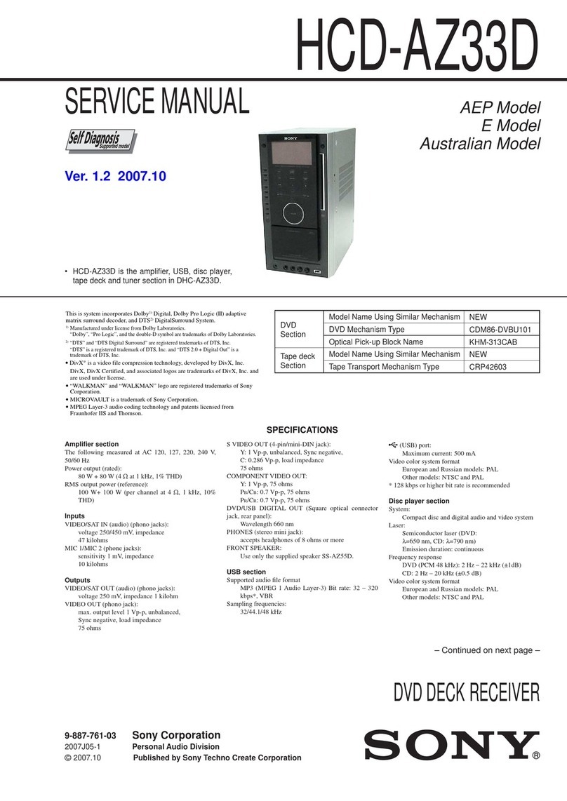
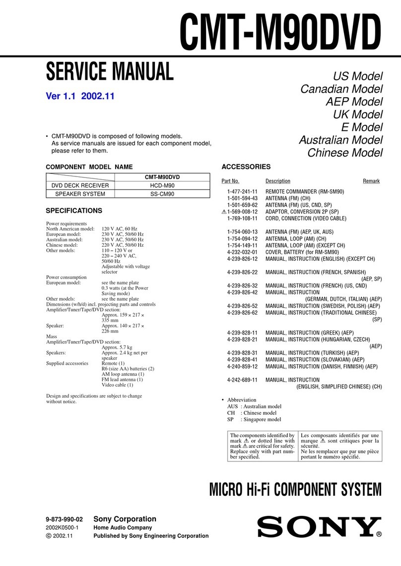
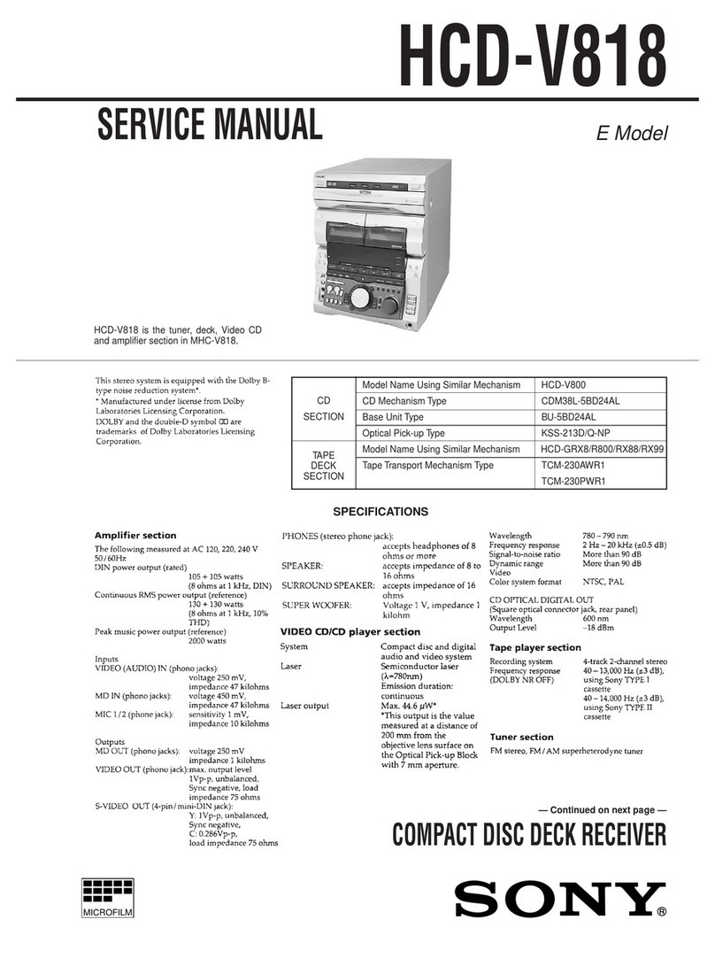
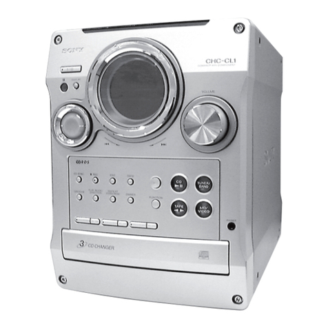
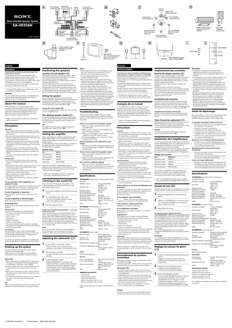
Sony ZS-X1 - Cd Boombox User manual

SERVICE MANUAL
PERSONAL AUDIO SYSTEM
US Model
Canadian Model
AEP Model
UK Model
E Model
Australian Model
SPECIFICATIONS
ZS-X1
Ver 1.2 2003.07
9-877-101-03 Sony Corporation
2003G05-1 Personal Audio Company
C2003.07 Published by Sony Engineering Corporation
Model Name Using Similar Mechanism NEW
CD Mechanism Type KSM-213RAP
Optical Pick-up Name KSS-213R
(US model only)
AUDIO POWER SPECIFICATIONS
POWER OUTPUT AND TOTAL
HARMONIC DISTORTION
With 3.2-ohm loads, both channels driven
from 150 - 10 000 Hz; rated 1.8 W per
channel-minimum RMS power, with no
more than 10 % total harmonic distortion
in AC operation.
Other specifications
CD player section
System
Compact disc digital audio system
Laser diode properties
Material: GaAlAs
Wave length: 780 nm
Emission duration: Continuous
Laser output: Less than 44.6 µW
(This output is the value measured at a distance
of about 200 mm from the objective lens surface
on the optical pick-up block with 7 mm
aperture.)
Spindle speed
200 r/min (rpm) to 500 r/min (rpm)
(CLV)
Number of channels
2
Frequency response
20 - 20 000 Hz +0/–1 dB
Wow and flutter
Below measurable limit
Radio section
Frequency range
FM: 87.5 - 108 MHz
AM: 530 - 1 710 kHz (US, Canadian models)
Antennas
FM: Telescopic antenna
AM/MW/LW: Built-in ferrite bar antenna
General
Speaker
Full range: 10 cm dia., 3.2 ohms, cone type (2)
Outputs
Headphones jack (stereo minijack)
For 16 - 64 ohms impedance headphones
Power output
2.3 W + 2.3 W (at 3.2 ohms, 10% harmonic
distortion)
Power requirements
DC IN 9V jack accepts:
Supplied AC power adaptor for use with
120 V AC, 60 Hz (US, Canadian)
220 V AC, 60 Hz (Korean)
230 V AC, 50 Hz (Australian)
240 V AC, 50 Hz (Others)
9 V DC, 6 size D (R20) batteries
Battery life
For personal audio system:
CD playback
Sony R20P: approx. 7.5 h
Sony alkaline LR20: approx. 14 h
Radio play
Sony R20P: approx. 11 h
Sony alkaline LR20: approx. 24 h
Dimensions
Approx. 430 ×175 ×288 mm (w/h/d)
(17 ×6
7
⁄
8
×11
3
⁄
8
inches)
(incl. projecting parts)
Mass
Approx. 3.5 kg (7 lb. 11 oz) (incl. batteries)
Supplied accessory
AC power adaptor(1)
Design and specifications are subject to change
without notice.
European model
MW 531 - 1 611 kHz (9 kHz step)
530 - 1 610 kHz (10 kHz step)
LW 153 - 279 kHz
Other models
AM 531 - 1 611 kHz (9 kHz step)
530 - 1 610 kHz (10 kHz step)

2
ZS-X1
ATTENTION AU COMPOSANT AYANT RAPPORT
À LA SÉCURITÉ!
LES COMPOSANTS IDENTIFIÉS PAR UNE MARQUE 0
SUR LES DIAGRAMMES SCHÉMATIQUES ET LA LISTE
DES PIÈCES SONT CRITIQUES POUR LA SÉCURITÉ
DE FONCTIONNEMENT. NE REMPLACER CES COM-
POSANTS QUE PAR DES PIÈCES SONY DONT LES
NUMÉROS SONT DONNÉS DANS CE MANUEL OU
DANS LES SUPPLÉMENTS PUBLIÉS PAR SONY.
SAFETY-RELATED COMPONENT WARNING!!
COMPONENTS IDENTIFIED BY MARK 0OR DOTTED
LINE WITH MARK 0ON THE SCHEMATIC DIAGRAMS
AND IN THE PARTS LIST ARE CRITICAL TO SAFE
OPERATION. REPLACE THESE COMPONENTS WITH
SONY PARTS WHOSE PART NUMBERS APPEAR AS
SHOWN IN THIS MANUAL OR IN SUPPLEMENTS PUB-
LISHED BY SONY.
Notes on chip component replacement
•Never reuse a disconnected chip component.
•Notice that the minus side of a tantalum capacitor may be dam-
aged by heat.
Flexible Circuit Board Repairing
•Keep the temperature of the soldering iron around 270 ˚C dur-
ing repairing.
•Do not touch the soldering iron on the same conductor of the
circuit board (within 3 times).
•Be careful not to apply force on the conductor when soldering
or unsoldering.
SAFETY CHECK-OUT
After correcting the original service problem, perform the follow-
ing safety check before releasing the set to the customer:
Check the antenna terminals, metal trim, “metallized” knobs,
screws, and all other exposed metal parts for AC leakage.
Check leakage as described below.
LEAKAGE TEST
The AC leakage from any exposed metal part to earth ground and
from all exposed metal parts to any exposed metal part having a
return to chassis, must not exceed 0.5 mA (500 microamperes).
Leakage current can be measured by any one of three methods.
1. A commercial leakage tester, such as the Simpson 229 or RCA
WT-540A. Follow the manufacturers’instructions to use these
instruments.
2. A battery-operatedAC milliammeter. The Data Precision 245
digital multimeter is suitable for this job.
3. Measuring the voltage drop across a resistor by means of a
VOM or battery-operated AC voltmeter. The “limit” indica-
tion is 0.75 V, so analog meters must have an accurate low-
voltage scale. The Simpson 250 and Sanwa SH-63Trd are ex-
amples of a passive VOM that is suitable. Nearly all battery
operated digital multimeters that have a 2VAC range are suit-
able. (See Fig. A)
Fig. A. Using an AC voltmeter to check AC leakage.
1.5 k
Ω
0.15 µFAC
voltmeter
(0.75 V)
To Exposed Metal
Parts on Set
Earth Ground
CAUTION
Use of controls or adjustments or performance of procedures
other than those specified herein may result in hazardous ra-
diation exposure.
About CD-Rs/CD-RWs
This player can play CD-Rs/CD-RWs
recorded in the CD-DA format*, but
playback capability may vary depending on
the quality of the disc and the condition of
the recording device.
* CD-DA is the abbreviation for Compact
Disc Digital Audio. It is a recording
standard used for Audio CDs.
On power sources
•For AC operation,
use the supplied
AC power
adaptor; do not
use any other type.
• The player is not disconnected from the
AC power source (mains) as long as it is
connected to the wall outlet, even if the
player itself has been turned off.
• Unplug the player from the wall outlet
when it is not to be used for an extended
period of time.
•For battery operation, use six size D (R20)
batteries.
• When the batteries are not to be used,
remove them to avoid damage that can be
caused by battery leakage or corrosion.
• The nameplate indicating operating
voltage, etc. is located at the bottom.
Polarity of
the plug
UNLEADED SOLDER
Boards requiring use of unleaded solder are printed with the lead-
free mark (LF) indicating the solder contains no lead.
(Caution: Some printed circuit boards may not come printed with
the lead free mark due to their particular size)
: LEAD FREE MARK
Unleaded solder has the following characteristics.
•Unleaded solder melts at a temperature about 40 ˚C higher than
ordinary solder.
Ordinary soldering irons can be used but the iron tip has to be
applied to the solder joint for a slightly longer time.
Soldering irons using a temperature regulator should be set to
about 350 ˚C.
Caution: The printed pattern (copper foil) may peel away if the
heated tip is applied for too long, so be careful!
•Strong viscosity
Unleaded solder is more viscou-s (sticky, less prone to flow)
than ordinary solder so use caution not to let solder bridges oc-
cur such as on IC pins, etc.
•Usable with ordinary solder
It is best to use only unleaded solder but unleaded solder may
also be added to ordinary solder.

3
ZS-X1
TABLE OF CONTENTS
1. SERVICING NOTES .............................................. 4
2. GENERAL .................................................................. 5
3. DISASSEMBLY
3-1. Disassembly Flow ........................................................... 6
3-2. Cabinet Lower Assy, Telescopic Antenna (ANT1) ........ 7
3-3. Main Chassis Section ...................................................... 8
3-4. AUDIO Board, BATTERY Board .................................. 8
3-5. TUNER Board, CONTROL Board................................. 9
3-6. CD Mechanism Deck Section......................................... 10
3-7. Optical Pick-up (KSS-213R) .......................................... 10
3-8. Cabinet Front Section ..................................................... 11
3-9. Speaker (10cm) (L) (SP101),
Speaker (10cm) (R) (SP201) .......................................... 11
3-10. Lid CD Assy .................................................................... 12
4. TEST MODE .............................................................. 13
5. ELECTRICAL ADJUSTMENTS
Tuner Section ................................................................. 14
CD Section ..................................................................... 15
6. DIAGRAMS
6-1. Block Diagram – CD Section – .................................... 16
6-2. Block Diagram – TUNER Section – ............................ 17
6-3. Block Diagram – MAIN Section – ............................... 18
6-4. Note for Printed Wiring Boards and
Schematic Diagrams ....................................................... 19
6-5. Printed Wiring Board – CD Section – .......................... 20
6-6. Schematic Diagram – CD Section – ............................. 21
6-7. Printed Wiring Board – TUNER Section
(US, CND, SP, KR, AUS models) – .............................. 22
6-8. Schematic Diagram – TUNER Section
(US, CND, SP, KR, AUS models) – .............................. 23
6-9. Printed Wiring Board
– TUNER Section (AEP, UK, IT, EE models) – ........... 24
6-10. Schematic Diagram
– TUNER Section (AEP, UK, IT, EE models) – ........... 25
6-11. Printed Wiring Boards
– AUDIO/POWER Section – ......................................... 26
6-12. Schematic Diagram – AUDIO/POWER Section –....... 27
6-13. Printed Wiring Boards – CONTROL Section – ........... 28
6-14. Schematic Diagram – CONTROL Section –................ 29
6-15. Schematic Diagram – LCD/KEY Section – ................. 30
6-16. IC Pin Function Description .......................................... 33
7. EXPLODED VIEWS
7-1. Cabinet Lower Section.................................................... 35
7-2. Cabinet Front Section ..................................................... 36
7-3. Cabinet Upper Section-1................................................. 37
7-4. Cabinet Upper Section-2................................................. 38
7-5. Cabinet Upper Section-3................................................. 39
7-6. Main Chassis Section ...................................................... 40
7-7. CD Block Section ........................................................... 41
7-8. Optical Pick-up Section (KSM-213RAP) ...................... 42
8. ELECTRICAL PARTS LIST .............................. 43
Ver 1.1
•Abbreviation
AUS:Australian model
CND : Canadian model
EE : East European model
IT : Italian model
KR : Korean model
SP : Singapore model

4
ZS-X1 SECTION 1
SERVICING NOTES
The laser diode in the optical pick-up block may suffer electro-
static break-down because of the potential difference generated
by the charged electrostatic load, etc. on clothing and the human
body.
During repair, pay attention to electrostatic break-down and also
use the procedure in the printed matter which is included in the
repair parts.
The flexible board is easily damaged and should be handled with
care.
NOTES ON LASER DIODE EMISSION CHECK
The laser beam on this model is concentrated so as to be focused
on the disc reflective surface by the objective lens in the optical
pick-up block. Therefore, when checking the laser diode emis-
sion, observe from more than 30 cm away from the objective lens.
LASER DIODE AND FOCUS SEARCH OPERATION
CHECK
During normal operation of the equipment, emission of the laser
diode is prohibited unless the upper lid is closed while turning ON
the S801. (push switch type)
The following checking method for the laser diode is operable.
•Method
Emission of the laser diode is visually checked.
1. Open the upper lid.
2. Push the S801 as shown in Fig.1.
Note: Do not push the detection lever strongly, or it may be bent or dam-
aged.
3. Check the object lens for confirming normal emission of the
laser diode. If not emitting, there is a trouble in the automatic
power control circuit or the optical pick-up.
In this operation, the object lens will move up and down 4
times along with inward motion for the focus search.
NOTES ON HANDLING THE OPTICAL PICK-UP
BLOCK OR BASE UNIT
S801
Fig.1 Method to push the S801

5
ZS-X1
SECTION 2
GENERAL This section is extracted from
instruction manual.
To turn on/off the power
European model: Press OPERATE.
Other models: Press POWER.
To adjust the volume
Press VOL +, –.
To listen through headphones
Connect the headphones to the i(headphones) jack.
Adjusting the sound emphasis
To reinforce the bass sound
Press MEGA BASS.
“MEGA BASS” appears in the display.
To return to normal sound, press the button again.
Location of controls
Total track number Programmed track Playing order
CD
Total playing time
Display/Visor
MEGA BASS
VOL –, +*
DISPLAY/ENT
MEMORY
MODE
i
x
u*
POWER
(US, CND, SP, KR, AUS models)
OPERATE
(AEP, UK, IT, EE models)
DC IN 9V
OPR/BATT
Loading a CD
With the labeled side up
ESP
BAND
AUTO PRESET
ESP indicator
Indicador ESP
Display
Visor *The button has a tactile dot.
ZPUSH
OPEN/CLOSE
Note
When inserting a CD, place the player horizontally.
If the player is not level, you cannot open or close the CD compartment lid.
•Abbreviation
AUS:Australian model
CND : Canadian model
EE : East European model
IT : Italian model
KR : Korean model
SP : Singapore model
Ver 1.1

ZS-X1
6
• This set can be disassembled in the order shown below.
3-1. DISASSEMBLY FLOW
SECTION 3
DISASSEMBLY
3-2. CABINET LOWER ASSY,
TELESCOPIC ANTENNA (ANT1)
(Page 7)
3-3. MAIN CHASSIS SECTION
(Page 8)
3-4. AUDIO BOARD,
BATTERY BOARD
(Page 8)
3-5. TUNER BOARD,
CONTROL BOARD
(Page 9)
3-6. CD MECHANISM
DECK SECTION
(Page 10)
3-7. OPTICAL PICK-UP
(KSS-213R)
(Page 10)
3-8. CABINET FRONT SECTION
(Page 11)
3-9. SPEAKER (10cm) (L) (SP101),
SPEAKER (10cm) (R) (SP201)
(Page 11)
3-10.LID CD ASSY
(Page 12)
SET

ZS-X1
7
Note: Follow the disassembly procedure in the numerical order given.
3-2. CABINET LOWER ASSY, TELESCOPIC ANTENNA (ANT1)
1
Open the CD lid.
2
screw
(BVTP3
×
14)
3
battery case
lid
4
two screws
(BVTP3
×
14)
4
five screws
(BVTP3
×
14)
4
five screws
(BVTP3
×
14)
6
cabinet lower
assy
7
telescopic antenna
(ANT1)
A
!
telescopic antenna
(ANT1)
main chassis
Note: Install the telescopic antenna with engaging
the
!
portion to the main chassis, then
check that the antenna is engaged and
does not move even trying to rotate it
in the direction of arrow
A
.
5
screw
(B3
×
8)

ZS-X1
8
5
audio board
4
three screws
(BVTP3
×
10)
2
two terminals
1
wire (
flat type) (18 core
)
(CN301)
3
connector
(CN901)
9
battery board
8
claw
6
Remove the connector lead wire
from the incision.
7
terminal
3-3. MAIN CHASSIS SECTION
6
wire (
flat type) (14 core)
(CN804)
5
wire (
flat type) (27 core)
(CN803)
3
four screws
(BVTP3
×
10)
7
main chassis section
4
1
connector (CN302)
2
connector (CN303)
3-4. AUDIO BOARD, BATTERY BOARD

ZS-X1
9
3-5. TUNER BOARD, CONTROL BOARD
3
two convex portions
2
8
1
screw
(BVTP3
×
10)
6
tuner board
4
connector
(CNP1)
5
terminal
9
Remove the lead wire
s
from the incision.
7
Remove the connector lead wires
from the incision.
qa
two screws
(BVTP3
×
10)
qd
control board
0
wire (
flat type) (18 core)
(CN301)
qs
two claws

ZS-X1
10
3-6. CD MECHANISM DECK SECTION
3-7. OPTICAL PICK-UP
(KSS-213R)
5
CD mechanism deck section
1
flexible flat cable (14P)
(CN702)
2
two
screws
(PWH2.6
×
10)
3
two
screws
(PWH2.6
×
10)
4
tension spring (CD)
4
gear (A)
5
two screws
(M2)
7
flexible flat cable
8
sled shaft
3
CD cover
1
two claws
2
two claws
9
optical pick-up
(KSS-213R)
6

ZS-X1
11
3-8. CABINET FRONT SECTION
3-9. SPEAKER (10cm) (L) (SP101), SPEAKER (10cm) (R) (SP201)
2
cabinet front section
1
two screws
(BVTP3
×
10)
1
two screws
(BVTP3
×
10)
0
Remove two solders.
5
Remove two solders.
qs
speaker (10cm) (L)
(SP101)
7
speaker (10cm) (R) (SP201)
qd
cabinet front sub assy
9
holder front (L)
4
holder front (R)
2
handle cover
qa
four screws
(BVTP3
×
10)
6
four screws
(BVTP3
×
10)
8
three screws
(BVTP3
×
10)
3
three screws
(BVTP3
×
10)
1
five screws
(BVTP3
×
10)

ZS-X1
12
– bottom view –
– bottom view –
1
screw (BVTP3
×
10)
3
damper
2
plate (SE)
5
boss
6
boss
8
lid
CD assy
7
4
CD spring
CD spring
lid
CD assy
lid
CD assy
cabinet upper
cabinet upper
3-10. LID CD ASSY

13
ZS-X1
SECTION 4
TEST MODE
CD TEST MODE
procedure:
1. Insert the disc (YEDS-18) (Part No. 3-702-101-01) (CD) or
(TCD-W082L) (Part No. J-2502-063-2) (CD-RW).
2. Press the [POWER] or [OPERATE] button to turn the power
on. (TOC read ended)
3. Set the test mode by momentarily shorting both of TAP (TEST-
A) on the LCD board. (The message “88” is displayed on the
liquid crystal display)
4. To release the test mode, press the [POWER] or [OPERATE]
button to turn the power off.
LCD TEST MODE
procedure:
1. Press the [POWER] or [OPERATE] button to turn the power
on.
2. Set the test mode by momentarily shorting both of TAP (TEST-
B) on the LCD board.
LCD DISPLAY
3. It repeats until any button is pressed.
Connecting Location:
– LCD BOARD (Conductor Side) –
TEST A
TEST B
1All lighting (4 seconds)
r
2COM0 lighting (2 seconds)
r
3COM1 lighting (2 seconds)
r
4COM2 lighting (2 seconds)
r
5COM3 lighting (2 seconds)
t
Ver 1.1

14
ZS-X1
AM (MW/LW) IF ADJUSTMENT
Adjust for a maximum reading on level meter
T1 450 kHz
(): Singapore, Korean, Australian models
AM VCO VOLTAGE ADJUSTMENT (US, CND, SP, KR, AUS)
Adjustment Part Frequency Display Reading on Digital Voltmeter
L4 530 (531) kHz 1.0 ±0.05 V
Confirmation 1,710 (1,611) kHz 5.3 (4.8) ±0.7 V
(): Singapore, Korean, Australian models
AM TRACKING ADJUSTMENT (US, CND)
Adjust for a maximum reading on level meter
L3 620 (621) kHz
CT3 1,400 (1,404) kHz
MW VCO VOLTAGE ADJUSTMENT (AEP, UK, IT, EE)
Frequency Display Reading on Digital Voltmeter
531 kHz 0.9 ±0.4 V
1,611 kHz 5.2 ±0.5 V
MW TRACKING ADJUSTMENT (AEP, UK, IT, EE)
Adjust for a maximum reading on level meter
L3-1 621 kHz
CT3 1,404 kHz
LW VCO VOLTAGE ADJUSTMENT (AEP, UK, IT, EE)
Adjustment Part Frequency Display Reading on Digital Voltmeter
L4 153 kHz 0.6 ±0.2 V
Confirmation 279 kHz 5.0 ±0.1 V
LW TRACKING ADJUSTMENT (AEP, UK, IT, EE)
Adjust for a maximum reading on level meter
L3-2 162 kHz
CT5 261 kHz
FM IF ADJUSTMENT
Adjust for a minimum reading on level meter
T2 10.7 MHz
FM VCO VOLTAGE ADJUSTMENT
Adjustment Part Frequency Display Reading on Digital Voltmeter
L2 108 MHz 3.0 ±0.2 V
Confirmation 87.5 MHz 1.3 ±0.3 V
FM TRACKING ADJUSTMENT
Adjust for a maximum reading on level meter
L1 87.5 MHz
CT1 108 MHz
Adjustment and Connecting Location: TUNER board
(See page 15)
TUNER SECTION 0 dB=1 µV
[AM (MW/LW) ]
Setting:
Function: RADIO
Band: AM (US, CND, SP, KR, AUS)
MW or LW (AEP, UK, IT, EE)
[FM]
Setting:
Function: RADIO
Band: FM
•Repeat the procedures in each adjustment several times, and the
tracking adjustments should be finally done by the trimmer ca-
pacitors.
•Remove FM antenna in FM adjustment.
AM RF signal
generator
30% amplitude
modulation by
400 Hz signal
Output level:
as low as possible
Put the lead-wire
antenna close to
the set.
+
–
level meter
set
3.2 Ω
AUDIO board
CN302 pin 2
AUDIO board
CN302 pin 1
FM RF signal
generator
75 kHz frequency
deviation by 1 kHz
signal
Output level:
as low as possible
+
–
level meter
AUDIO board
CN302 pin 2
AUDIO board
CN302 pin 1
set
3.2 Ω
0.01 µF
TUNER board
TP (GND)
TUNER board
TP (ANT)
digital voltmete
r
TP (VT)
TP (GND)
100 kΩ
TUNER board
SECTION 5
ELECTRICAL ADJUSTMENTS
PRECAUTION
1. Setting
MEGA BASS : OFF
Ver 1.1

ZS-X1
1515
FOCUS BIAS CHECK
procedure:
1. Connect the oscilloscope to TP (RF) and TP (VC) on the CD
board.
2. Set the CD test mode. (Refer to CD TEST MODE (See page
13))
3. Press the ubutton twice. (LCD DISPLAY “P –”)
Note: If this check is performed continuously after the
TRAVERSE CHECK, press the ubutton once.
4. Confirm that the oscilloscope waveform is as shown in the
figure below. (eye pattern)
A good eye pattern means that the diamond shape (◊) in the
center of the waveform can be clearly distinguished.
5. To check CD-RW, turn the power off. Change discs to CD-
RW (TCD-W082L) (Part No. J-2502-063-2), then set the CD
test mode again. (Refer to CD TEST MODE (See page 13))
• RF signal reference waveform (eye pattern)
Connecting Location:
CD SECTION
Perform all CD section check in the test mode.
TRAVERSE CHECK
procedure:
1. Connect an oscilloscope to TP (TE) and TP (VC) on the CD
board.
2. Set the CD test mode. (Refer to CD TEST MODE (See page
13))
3. Press the ubutton once. (LCD DISPLAY “F –”)
4. Confirm that the center of the oscilloscope waveform is at 0V.
5. Confirm that the oscilloscope waveform Vp-p value is at 0.95
±0.4 V.
6. To check CD-RW, turn the power off. Change discs to CD-
RW (TCD-W082L) (Part No. J-2502-063-2), then set the CD
test mode again. (Refer to CD TEST MODE (See page 13))
VOLT/DIV: 0.2 V (with the 10: 1 probe in use.)
TIME/DIV: 500 ns
CD:
1.0
±
0.3 Vp-p
CD-RW:
1.0
±
0.4 Vp-p
When observing the eye pattern, set the oscilloscope
for AC range and raise vertical sensitivity.
VOLT/DIV:0.2 V (with the 10:1 probe in use)
TIME/DIV: 1 ms
0 V A
BVp-p=A+
B
– CD BOARD (Conductor Side) –
TP
(TE)
TP
(VC)
TP
(RF)
Adjustment and Connecting Location:
–TUNER BOARD (Component Side) (US, CND, SP, KR, AUS) –
–TUNER BOARD (Conductor Side) –
L4
AM VCO Voltage Adjustment
L2
FM VCO Voltage Adjustment
AM Tracking Adjustment CT3
L3
FM Tracking Adjustmen
t
T1 AM IF Adjustment
T2 FM IF Adjustment
L1
CT1
–TUNER BOARD (Component Side) (AEP, UK, IT, EE) –
L4
LW VCO Voltage Adjustment
L2
FM VCO Voltage Adjustment
LW Tracking Adjustment CT3
L3-2
FM Tracking Adjustmen
t
T1 AM IF Adjustment
T2 FM IF Adjustment
L1
CT1
MW Tracking Adjustment
CT3
L3-1
TP
(VT)
TP
(GND)
TP
(ANT)
•Abbreviation
AUS:Australian model
CND : Canadian model
EE : East European model
IT : Italian model
KR : Korean model
SP : Singapore model
Ver 1.1

ZS-X1
1616
SECTION 6
DIAGRAMS
6-1. BLOCK DIAGRAM – CD Section –
SYSTEM
CONTROLLER
IC802 (1/2)
PD (I)
: CD PLAY
•R-ch is omitted due to same as L-ch.
•SIGNAL PATH
A
B
D
F
E
C
I-V AMP
DETECTOR
LD
PD
LASER DIODE
OPTICAL PICK-UP
BLOCK
(KSM-213RAP)
2-AXIS
DEVICE
(TRACKING)
(FOCUS)
A
D
C
B
F
E
LD
PD
F+
F–
T+
T–
3BD (I)
6F (I)
2AC (I)
RF SIGNAL
GENERATOR
100 99
EQO (O)
RFI (I)
9FEO (O)
5E (I)
8FEN (I)
96 TEO (O)
97 TEN (I)
AUTOMATIC
POWER
CONTROL
Q701
13 LD (O) APC
12
DIGITAL
SIGNAL
PROCESSOR
17
18
12
11
27 SL+
SL–
T–
T+
F+
F–
SPINDLE
MOTOR DRIVE
M701
(SPINDLE)
SLED
MOTOR DRIVE
26
M702
(SLED)
TRACKING
COIL DRIVE
FOCUS
COIL DRIVE
SP+
SP– 3
24
20
9
TIN
(FIN) 14 OPOUT FOCUS
COIL DRIVE 15
OPIN
(SLIN)
SPIN
FOCUS/TRACKING COIL DRIVE,
SPINDLE/SLED MOTOR DRIVE
IC703
2
1
M
M
7MUTE
FOCUS GAIN
UP SWITCH
Q705
FOCUS GAIN
UP SWITCH
Q704
16M BIT SD-RAM
IC702
ANTI-SHOCK
MEMORY CONTROLLER
DIGITAL SERVO
SIGNAL PROCESSOR
56 – 71 41 – 52
19 – 24, 27 – 32
2, 3, 5, 6, 8, 9, 11, 12, 39,
40, 42, 43, 45, 46, 48, 49
RCLK (O)
DQ00 – DQ15
DQ0 – DQ15
A00 (O) – A11 (O)
A0 – A11
CLK
35
RCKE (O)
CKE
34
WEX (O)
WE
15
CASX (O)
CAS
16
RASX (O)
RAS
17
37 38 55 54 53
16K SRAM
FOCUS GAIN
CONTROL SWITCH
Q703
21
TDOUT (O)
20
JUMPO (O)
23
SDOUT (O)
24
CLVOUT (O)
19
FDOUT (O)
91
XPLCK
88
DFDIN (I)
RESETX
33
RW (I)
30
MCK (I)
31
DIN (I)
32
DOUT (O)
53 C-DOUT (I)
54 C-DIN (O)
55 C-MCK (O)
62 C-RW (O)
64 C-RESETX (O)
61 C-BUSY (I)
52 C-SUBSYQ (I)
COMMAND
INTERFACE
D703
34
1BIT
D/A CONVERTER
80
LDACO
82
RDACO
CD-LOUT
RF AMP, FOCUS/TRACKING SERVO,
DIGITAL SIGNAL PROCESSOR,
DIGITAL SERVO SIGNAL PROCESSOR,
DIGITAL FILTER, D/A CONVERTER,
ANTI-SHOCK MEMORY CONTROLLER
IC701
(Page 18)
A
R-CH
X8 OVER
SAMPLIMG
DIGITAL FILTER
DIGITAL SERVO
FILTER
SERVO
SIGNAL
GENERATOR
XI (I)
XO (O)
X701
16.9344MHz
77
BUSY 35
SUBSYQ 29
76
MONI0
MONI1 90
89
ERROR
MONITOR
Q702
29
C-DOOR
S801
PUSH OPEN/CLOSE
63 C-LIM SW (I)
When the optical pick-up
is inner position
ON :
S701
(LIMIT)

ZS-X1
1717
6-2. BLOCK DIAGRAM – TUNER Section –
2
24
4 7
20 21
FM
RF AMP
FM
MIX
FM
OSC
FM IF
AMP
IF
BUFFER
AF
BUFFER
AF
AMP MPX MUTE
STEREO/
MONO,
FM/AM
AM IF
AMP
FM
DET
AM
DET
6
FM
RF-IN
22 AM
RF AMP
Q14
AM
MIX
AM
RF-IN
MIX-OUT
OSC
-OUT
CF2
FM/AM PLL
IC2
(US, CND, SP, KR, AUS) (AEP, UK, IT, EE)
CF4
FM
RF-OUT
10
QUAD
FM
IF-IN 12
15
11
L-OUT
MPX
-IN
R-OUT
13
AM
IF-IN
LPF1/BAND
AM OSC
FM OSC
FM/AM RF AMP, MIX, OSC,
FM/AM IF AMP, DET, MPX
IC1
(US, CND, SP, KR, AUS) (AEP, UK, IT, EE)
L2
FM VCO VOLTAGE
CT1, L1
FM TRACKING
CT3, L3
AM TRACKING
T1
AM IFT
LOW-PASS
FILTER
LOW-PASS
FILTER
• SIGNAL PATH
: FM
: AM (MW/LW)
X1
75kHz
CT3
L1
FM RF
XOUT
XIN
AM IN
IF IN
ST-IND
LP-OUT
LP-IN
FM IN
20
19
111218
MW/LW
6
CT1
D1
L4
AM (MW/LW)
OSC
L2
FM OSC
LEVEL
DET
ST
IND
14
LPF2/MO-ST
AM
OSC BUFFER
BUFFER
SWALLOW
COUNTER
UNIVERSAL
COUNTER
CCB
INTERFACE
REFERENCE
DIVIDER
UNLOCK
DETECT
12 BIT
PROGRAMMABLE
DIVIDER
PHASE
DETECTOR/
CHARGE PUMP
SHIFT REGISTER & LATCH
1/2
BAND
DI
CL
CE
DO
DET
-OUT
ANT1
FM TELESCOPIC
ANTENNA
PD
IF-OUT
ST-IND
2
3
1
4
10 9
BAND
7
MO/ST
13817 16
17 18
16
19
CT5
D2
(AEP, UK, IT, EE)
(US, CND, SP, KR, AUS)
D3
(1/2)
D3
(2/2)
AM HIGH
CUT
SWITCH
Q12
T1
AM IF
Q42
Q41
CD/RADIO
+6.2V
Q41, 42
MW SWITCH
L3-1
MW
L3-2
LW
L3
MW/LW
FERRITE-ROD
ANTENNA
MW
TRACKING
CT3, L3-1
LW
TRACKING
CT5, L3-2
LW
SWITCH
Q44
LW SWITCH
Q43
• R-ch is omitted due to same as L-ch.
R DATA
R CLOCK
R CE
R COUNT
R-CH
(Page 18)
C
B MUTE
TU-LCH
(Page 18)
B
CONSTANT
CURRENT
Q61
T2
FM IFT
T2
FM IF
L3
AM FERRITE-ROD
ANTENNA
(AEP, UK, IT, EE)
(AEP, UK, IT, EE)
(US, CND, SP, KR, AUS)
R DATA, R CLOCK, R CE,
R COUNT, B MUTE
(AEP, UK, IT, EE)
(US, CND, SP, KR, AUS)
(AEP, UK, IT, EE)
(US, CND, SP, KR, AUS)
L4
AM VCO VOLTAGE
L4
LW VCO VOLTAGE
• Abbrivation
AUS : Australian model
CND : Canadian model
EE : East European model
IT : Italian model
KR : Korean model
SP : Singapore model
D301
SW +9V
MUTING
SWITCH
Q806
Ver 1.1

ZS-X1
1818
6-3. BLOCK DIAGRAM – MAIN Section –
: CD PLAY
: TUNER (FM/AM)
MEGA BASS
CONTROL SWITCH
Q121
76RST
36CD
39BTT-CHK-H
65P-CON
40BTT-CHK-M
SYSTEM CONTROLLER
IC802 (2/2)
+6.2V
REGULATOR
Q904
+6.2V
REGULATOR
Q903
+3.3V
REGULATOR
Q907
B+ SWITCH
Q901, 902
B+ SWITCH
Q303
DRY BATTERY
SIZE“D”
(IEC DESIGNATION R20)
6PCS. 9V
+3.3V
REGULATOR
IC801
RESET SIGNAL
GENERATOR
IC804
DC IN 9V
J901
–+
CD +6.2V
D401
POWER
AMP B+
U-COM +3.3V
CD +3.3V
SW +9V
ELECTRICAL
VOLUME B+
TU +6.2V
DC LEVEL
DETECT
Q802, 803
ESP LED 426V REG
51LOAD
R-CH
R-CH
SP101
(L-CH)
SP201
(R-CH)
J301
i
LINE AMP
Q102 1
LOGIC
CONTROL
4 5
2
ELECTRICAL VOLUME
IC301
D131 D231
•R-ch is omitted due to same as L-ch.
•SIGNAL PATH
VIN1 VOUT1
DATA
CLOCK
R-CH
D321
MUTING
Q122
LINE AMP
Q101
TU-LCH
B
(Page 17)
CD-LOUT
A
(Page 16)
D402
ESP
R-DATA
R-CLK
R-LAT
R-COUNT
59
57
58
56
(Page 17)
C
B-MUTE
60
433.3V REG
S0 – S16
LIQUID CRYSTAL DISPLAY
LCD401
10 – 26
COM0 – COM3
6 – 9
66
SDA
SCL
5 6
SDA
SCL
EEPROM
IC803
80 79
R DATA
R CLOCK
R CE
R COUNT
B MUTE
V-CLK
77
V-DATA
78
A-MUTE
35
DBB
68
+
SW +9V
POWER AMP
IC302
11 POWER
AMP 5
8
ST-BY
R DATA, R CLOCK, R CE,
R COUNT, B MUTE
WAKE UP
SWITCH
Q804
KEY 2
S401 – 406
44
KEY 1
S407 – 414
45
WP/INI
50
MODE
DETECT
Q805
MODE CHK
46
D801
7071
X801
32.768kHz
7475
X802
4.19MHz
XT1
XT2
X1
X2
REGULATOR
CONTROL SWITCH
Q905, 906
D302
TUNER ON
SWITCH
Q301, 302
LOAD CONTROL
SWITCH
Q809, 810
OPR/BATT
DC LEVEL
DETECT
Q801, 811
LED DRIVE
Q807, 808

ZS-X1
1919
6-4. NOTE FOR PRINTED WIRING BOARDS AND SCHEMATIC DIAGRAMS
Note on Schematic Diagram:
•All capacitors are in µF unless otherwise noted. pF: µµF
50 WV or less are not indicated except for electrolytics
and tantalums.
•All resistors are in Ωand 1/4W or less unless otherwise
specified.
•f: internal component.
•C: panel designation.
•A: B+ Line.
•H: adjustment for repair.
•Power voltage is dc 9 V and fed with regulated dc power
supply from pin 2and 3of CN902 on the BATTERY
board.
no mark : FM
(): AM (MW)
{}:LW
[]:CD PLAY
〈〈 〉〉 : CD STOP
∗: Impossible to measure
•Voltages aretakenwith aVOM (Inputimpedance 10MΩ).
Voltage variations may be noted due to normal produc-
tion tolerances.
•Waveforms are taken with a oscilloscope.
Voltage variations may be noted due to normal produc-
tion tolerances.
•Circled numbers refer to waveforms.
•Signal path.
F: FM
f: AM (MW/LW)
J: CD PLAY
•Abbreviation
AUS:Australian model
CND : Canadian model
EE : East European model
IT : Italian model
KR : Korean model
SP : Singapore model
Note:
The components identi-
fied by mark 0or dotted
linewithmark 0are criti-
cal for safety.
Replace only with part
number specified.
Note:
Lescomposants identifiés par
une marque 0sont critiques
pour la sécurité.
Ne les remplacer que par une
pièce portant le numéro
spécifié.
Note on Printed Wiring Boards:
•X: parts extracted from the component side.
•Y: parts extracted from the conductor side.
•W: indicates side identified with part number.
•f: internal component.
•: Pattern from the side which enables seeing.
(The other layers' patterns are not indicated.)
Caution:
Pattern face side: Partsonthepatternfacesideseenfrom
(Conductor Side) the pattern face are indicated.
Parts face side: Parts on the parts face side seen from
(Component Side) the parts face are indicated.
•Circuit Boards Location
key board
CD board
jack boar
d
LCD board
tuner board
battery board
audio board
control board
Ver 1.1

ZS-X1
2020
13
IC702
R749
R750
R751
R773
R774
C744
IC701
R756
R755
C727
C726
C725
JC702
C706
R702
R706
R708
R704
R717 C755
C710 C709
R725
R726
C756
R772
R754
C757
C758
R760
C724
R782
R783
R784
R785
R786
C782
C783
R709
R713
JC701
Q704
Q705
C723
X701 C704
C719
C716
C722
C707
C761
C733
C703C701C747
S701
M701
M702
CN702
CN701
C759
IC703
R741
C721
R745
R721
R720
R724
R723
C702
Q701
R722
R765
R763
R764
Q702
R766
C752 R770
C754C753
C751
C750
R768
C708
C705
C714
C732
C746
C745
C738
R762
C769
C767 R775
R776
C766
C765
C764
C763
FB701
C735
C728
R757
R758
R759
C731
C713
C712
C711
R740
C718 R736
R734
R731
R730
R733 R732
R728
R729
C720
R727
C730
C729
C771
C772
C715
C762
FB702
C760
R739
R742
R743
R744
R746
C773
D703
Q703
R778
C717
R780
R781
R747
C774
C781
D704
C748
R761
C736
C737
FB707
1
25
75
51
26 50
100 76
(COMPONENT SIDE)
CD BOARD
1-687-005-
11
(11)
(CONDUCTOR SIDE)
CD BOARD
1-687-005-
11
(11)
K
A
OPTICAL
PICK-UP BLOCK
(KSM-213RAP)
(SLED)
(SPINDLE)
KA
(LIMIT)
ON : When the optical
pick-up is inner position
S701
B
CONTROL
BOARD
CN804
1 2 3 4 5 6 7 8 9 10 11 12 13 14 15 16
A
B
C
D
E
F
G
H
17 18
M
M
21
16 15
TP
(VC)
TP
(TE)
TP
(RF)
6-5. PRINTED WIRING BOARD – CD Section – • See page 19 for Circuit Boards Location. :Uses unleaded solder.
(Page 28)
D703 G-16
D704 B-14
IC701 F-6
IC702 E-8
IC703 E-17
Q701 B-14
Q702 B-13
Q703 B-14
Q704 F-3
Q705 E-3
•Semiconductor
Location
Ref. No. Location
Other manuals for ZS-X1 - Cd Boombox
3
Table of contents
Other Sony Stereo System manuals

Sony
Sony HCD-HP7 - Hi Fi Components User manual

Sony
Sony HCD-BX9 User manual

Sony
Sony HCD-EC909iP - Compact Disc Receiver... User manual

Sony
Sony CMT-CP505MD User manual

Sony
Sony Giga Juke NAS-SC500PK User manual

Sony
Sony SS-CHP7 User manual

Sony
Sony HCD-GR8000 User manual

Sony
Sony MHC-GNZ9D User manual

Sony
Sony ZS ZS-SN10L User manual

Sony
Sony MEX-BT3750U User manual