Spectrum Digital TMS320DM6437 Use and care manual

TMS320DM6437
Evaluation Module
2006 DSP Development Systems
Reference
Technical


TMS320DM6437 Evaluation
Module Technical Reference
509105-0001 Rev. C
December 2006
SPECTRUM DIGITAL, INC.
12502 Exchange Drive, Suite 440 Stafford, TX. 77477
Tel: 281.494.4505 Fax: 281.494.5310
sales@spectrumdigital.com www.spectrumdigital.com

IMPORTANT NOTICE
Spectrum Digital, Inc. reserves the right to make changes to its products or to discontinue any
product or service without notice. Customers are advised to obtain the latest version of relevant
information to verify that the data being relied on is current before placing orders.
Spectrum Digital, Inc. warrants performance of its products and related software to current
specifications in accordance with Spectrum Digital’s standard warranty. Testing and other quality
control techniques are utilized to the extent deemed necessary to support this warranty.
Please be aware that the products described herein are not intended for use in life-support
appliances, devices, or systems. Spectrum Digital does not warrant nor is Spectrum Digital liable for
the product described herein to be used in other than a development environment.
Spectrum Digital, Inc. assumes no liability for applications assistance, customer product design,
software performance, or infringement of patents or services described herein. Nor does Spectrum
Digital warrant or represent any license, either express or implied, is granted under any patent right,
copyright, or other intellectual property right of Spectrum Digital, Inc. covering or relating to any
combination, machine, or process in which such Digital Signal Processing development products or
services might be or are used.
WARNING
This equipment is intended for use in a laboratory test environment only. It generates, uses, and can
radiate radio frequency energy and has not been tested for compliance with the limits of computing
devices pursuant to subpart J of part 15 of FCC rules, which are designed to provide reasonable
protection against radio frequency interference. Operation of this equipment in other environments
may cause interference with radio communications, in which case the user at his own expense will be
required to take whatever measures necessary to correct this interference.
Copyright © 2006 Spectrum Digital, Inc.

Contents
1 Introduction to the DM6437 Evaluation Module . . . . . . . . . . . . . . . . . . . . . . . . . . . . . . . . 1-1
Provides you with a description of the DM6437 Evaluation Module, key features, and
block diagram.
1.1 Key Features . . . . . . . . . . . . . . . . . . . . . . . . . . . . . . . . . . . . . . . . . . . . . . . . . . . . . . . . . . 1-2
1.2 Functional Overview . . . . . . . . . . . . . . . . . . . . . . . . . . . . . . . . . . . . . . . . . . . . . . . . . . . . 1-3
1.3 Basic Operation . . . . . . . . . . . . . . . . . . . . . . . . . . . . . . . . . . . . . . . . . . . . . . . . . . . . . . . . . 1-4
1.4 Memory Map . . . . . . . . . . . . . . . . . . . . . . . . . . . . . . . . . . . . . . . . . . . . . . . . . . . . . . . . . . 1-5
1.5 Configuration Switch Settings . . . . . . . . . . . . . . . . . . . . . . . . . . . . . . . . . . . . . . . . . . . . . 1-6
1.6 Power Supply . . . . . . . . . . . . . . . . . . . . . . . . . . . . . . . . . . . . . . . . . . . . . . . . . . . . . . . . . 1-6
1.7 Power Measurement . . . . . . . . . . . . . . . . . . . . . . . . . . . . . . . . . . . . . . . . . . . . . . . . . . . 1-6
2 Board Components . . . . . . . . . . . . . . . . . . . . . . . . . . . . . . . . . . . . . . . . . . . . . . . . . . . . . . . . 2-1
Describes the operation of the major board components on the DM6437 Evaluation Module.
2.1 EMIF Interfaces . . . . . . . . . . . . . . . . . . . . . . . . . . . . . . . . . . . . . . . . . . . . . . . . . . . . . . . . . 2-2
2.1.1 DDR2 Memory Interface . . . . . . . . . . . . . . . . . . . . . . . . . . . . . . . . . . . . . . . . . . . . . . 2-2
2.1.2 Flash, NAND Flash, SRAM Memory Interface . . . . . . . . . . . . . . . . . . . . . . . . . . . . . . . 2-2
2.2 Peripheral Interfaces . . . . . . . . . . . . . . . . . . . . . . . . . . . . . . . . . . . . . . . . . . . . . . . . . 2-2
2.2.1 VLYNQ Interface . . . . . . . . . . . . . . . . . . . . . . . . . . . . . . . . . . . . . . . . . . . . . . . . . . 2-2
2.2.2 UART Interface . . . . . . . . . . . . . . . . . . . . . . . . . . . . . . . . . . . . . . . . . . . . . . . . . . 2-2
2.2.3 CAN Interface . . . . . . . . . . . . . . . . . . . . . . . . . . . . . . . . . . . . . . . . . . . . . . . . . . . . . 2-3
2.3 Video Interfaces . . . . . . . . . . . . . . . . . . . . . . . . . . . . . . . . . . . . . . . . . . . . . . . . . . . . . . . . 2-3
2.3.1 Input Video Port Interfaces . . . . . . . . . . . . . . . . . . . . . . . . . . . . . . . . . . . . . . . . . . . . . 2-3
2.3.2 On Chip Video Output DACs . . . . . . . . . . . . . . . . . . . . . . . . . . . . . . . . . . . . . . . . . . . . 2-3
2.4 AIC33 Interface . . . . . . . . . . . . . . . . . . . . . . . . . . . . . . . . . . . . . . . . . . . . . . . . . . . . . . . 2-4
2.4.1 Audio PLL/VCXO Circuit/PLL1705 Clock Generator . . . . . . . . . . . . . . . . . . . . . . . . . 2-5
2.5 Ethernet Interface . . . . . . . . . . . . . . . . . . . . . . . . . . . . . . . . . . . . . . . . . . . . . . . . . . . . . . . 2-6
2.6 I2C Interface . . . . . . . . . . . . . . . . . . . . . . . . . . . . . . . . . . . . . . . . . . . . . . . . . . . . . . . . . . . 2-6
2.6.1 I/O Expanders . . . . . . . . . . . . . . . . . . . . . . . . . . . . . . . . . . . . . . . . . . . . . . . . . . . . . . . . 2-7
2.6.2 I2C EEPROM . . . . . . . . . . . . . . . . . . . . . . . . . . . . . . . . . . . . . . . . . . . . . . . . . . . . . . . . 2-9
2.7 S/PDIF Analog, and Optical Interfaces . . . . . . . . . . . . . . . . . . . . . . . . . . . . . . . . . . . . 2-9
2.8 Daughter Card Interface . . . . . . . . . . . . . . . . . . . . . . . . . . . . . . . . . . . . . . . . . . . . . . . . 2-10
2.9 DM6437 Core CPU Clock . . . . . . . . . . . . . . . . . . . . . . . . . . . . . . . . . . . . . . . . . . . . . . 2-10
2.10 DM6437 Core Voltage Select . . . . . . . . . . . . . . . . . . . . . . . . . . . . . . . . . . . . . . . . . . 2-10

3 Physical Specifications . . . . . . . . . . . . . . . . . . . . . . . . . . . . . . . . . . . . . . . . . . . . . . . . . . . . 3-1
Describes the physical layout of the DM6437 Evaluation Module and its connectors.
3.1 Board Layout . . . . . . . . . . . . . . . . . . . . . . . . . . . . . . . . . . . . . . . . . . . . . . . . . . . . . . . . 3-3
3.2 Connectors . . . . . . . . . . . . . . . . . . . . . . . . . . . . . . . . . . . . . . . . . . . . . . . . . . . . . . . . 3-4
3.2.1 J1, DAC A Video Out . . . . . . . . . . . . . . . . . . . . . . . . . . . . . . . . . . . . . . . . . . . . . . . . . 3-5
3.2.2 J2, DAC B Video Out . . . . . . . . . . . . . . . . . . . . . . . . . . . . . . . . . . . . . . . . . . . . . . . . . . 3-5
3.2.3 J3, DAC C Video Out . . . . . . . . . . . . . . . . . . . . . . . . . . . . . . . . . . . . . . . . . . . . . . . . . . 3-5
3.2.4 J4, DAC A Video Out . . . . . . . . . . . . . . . . . . . . . . . . . . . . . . . . . . . . . . . . . . . . . . . . . . 3-6
3.2.5 J5, Video In . . . . . . . . . . . . . . . . . . . . . . . . . . . . . . . . . . . . . . . . . . . . . . . . . . . . . . . . . . 3-6
3.2.6 J10, S/PDIF Out . . . . . . . . . . . . . . . . . . . . . . . . . . . . . . . . . . . . . . . . . . . . . . . . . . . . . 3-7
3.2.7 J16, +5V Input . . . . . . . . . . . . . . . . . . . . . . . . . . . . . . . . . . . . . . . . . . . . . . . . . . . . . . . 3-7
3.2.8 J20, Mini PCI Interface . . . . . . . . . . . . . . . . . . . . . . . . . . . . . . . . . . . . . . . . . . . . . . . . 3-8
3.2.9 J501, Embedded Mini USB Emulation Interface . . . . . . . . . . . . . . . . . . . . . . . . . . . . 3-9
3.2.10 P1, Video Out . . . . . . . . . . . . . . . . . . . . . . . . . . . . . . . . . . . . . . . . . . . . . . . . . . . . . . 3-9
3.2.11 P2, Video In . . . . . . . . . . . . . . . . . . . . . . . . . . . . . . . . . . . . . . . . . . . . . . . . . . . . . . . 3-10
3.2.12 P3, Ethernet Interface . . . . . . . . . . . . . . . . . . . . . . . . . . . . . . . . . . . . . . . . . . . . . . . 3-10
3.2.13 P4, PCI Interface . . . . . . . . . . . . . . . . . . . . . . . . . . . . . . . . . . . . . . . . . . . . . . . . . . . 3-11
3.2.14 P7, CAN Connector . . . . . . . . . . . . . . . . . . . . . . . . . . . . . . . . . . . . . . . . . . . . . . . . . 3-13
3.2.15 P8, RS-232 UART . . . . . . . . . . . . . . . . . . . . . . . . . . . . . . . . . . . . . . . . . . . . . . . . . . 3-14
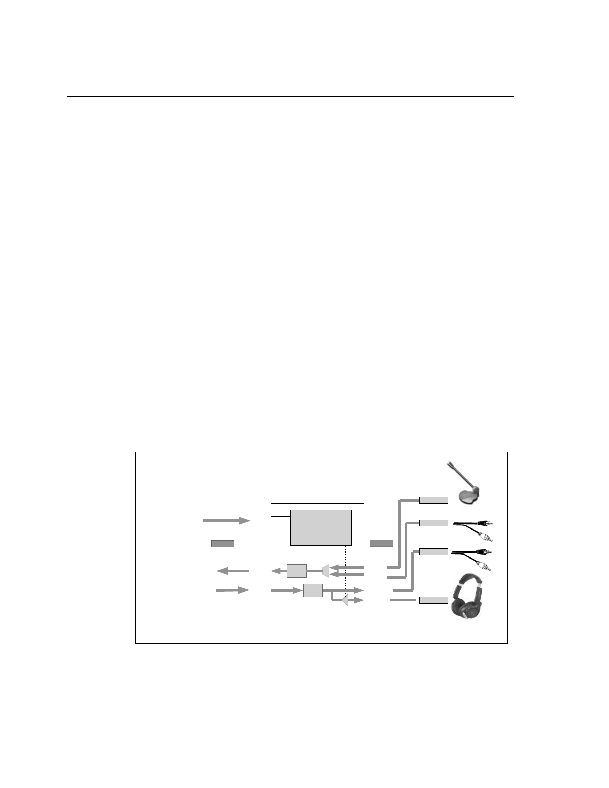
3.2.16 P10, Stereo Line In . . . . . . . . . . . . . . . . . . . . . . . . . . . . . . . . . . . . . . . . . . . . . . . . 3-15
3.2.17 P11, Microphone In . . . . . . . . . . . . . . . . . . . . . . . . . . . . . . . . . . . . . . . . . . . . . . . . . 3-15
3.2.18 P12, Headphone Out . . . . . . . . . . . . . . . . . . . . . . . . . . . . . . . . . . . . . . . . . . . . . . 3-15
3.2.19 P13, Stereo Line Out . . . . . . . . . . . . . . . . . . . . . . . . . . . . . . . . . . . . . . . . . . . . . . . . 3-16
3.2.20 P14, S/PDIF Out . . . . . . . . . . . . . . . . . . . . . . . . . . . . . . . . . . . . . . . . . . . . . . . . . . . 3-16
3.2.21 DC_P1, Memory/Video Expansion . . . . . . . . . . . . . . . . . . . . . . . . . . . . . . . . . . . . . 3-17
3.2.22 DC_P2, Peripheral Expansion . . . . . . . . . . . . . . . . . . . . . . . . . . . . . . . . . . . . . . . . 3-18
3.2.23 DC_P3, VLYNQ Connector . . . . . . . . . . . . . . . . . . . . . . . . . . . . . . . . . . . . . . . . . . 3-19
3.3 Jumpers . . . . . . . . . . . . . . . . . . . . . . . . . . . . . . . . . . . . . . . . . . . . . . . . . . . . . . . . . . . . 3-19
3.3.1 JP1 Jumper . . . . . . . . . . . . . . . . . . . . . . . . . . . . . . . . . . . . . . . . . . . . . . . . . . . . . . . . . 3-20
3.3.2 JP2 Jumper . . . . . . . . . . . . . . . . . . . . . . . . . . . . . . . . . . . . . . . . . . . . . . . . . . . . . . . . . 3-20
3.3.3 JP3 Jumper . . . . . . . . . . . . . . . . . . . . . . . . . . . . . . . . . . . . . . . . . . . . . . . . . . . . . . . . . 3-21
3.3.4 JP4 Jumper . . . . . . . . . . . . . . . . . . . . . . . . . . . . . . . . . . . . . . . . . . . . . . . . . . . . . . . . 3-21
3.4 LEDs . . . . . . . . . . . . . . . . . . . . . . . . . . . . . . . . . . . . . . . . . . . . . . . . . . . . . . . . . . . . . . . . 3-21
3.5 Switches . . . . . . . . . . . . . . . . . . . . . . . . . . . . . . . . . . . . . . . . . . . . . . . . . . . . . . . . . . . . . 3-22
3.5.1 SW1, Bootload Mode Selections . . . . . . . . . . . . . . . . . . . . . . . . . . . . . . . . . . . . . . . 3-22
3.5.2 SW2, Bootload Configuration Select . . . . . . . . . . . . . . . . . . . . . . . . . . . . . . . . . . . . 3-23
3.5.3 SW3, EMDATA Select . . . . . . . . . . . . . . . . . . . . . . . . . . . . . . . . . . . . . . . . . . . . . . . . 3-23
3.5.4 SW4, 4 Position User Readable . . . . . . . . . . . . . . . . . . . . . . . . . . . . . . . . . . . . . . . . 3-23
3.5.5 SW5, Power On Reset Switch . . . . . . . . . . . . . . . . . . . . . . . . . . . . . . . . . . . . . . . . . . 3-23
3.5.6 SW6, Reset Switch . . . . . . . . . . . . . . . . . . . . . . . . . . . . . . . . . . . . . . . . . . . . . . . . . . 3-23
3.5.7 SW7, Slide Switch . . . . . . . . . . . . . . . . . . . . . . . . . . . . . . . . . . . . . . . . . . . . . . . . . . 3-24
3.6 Test Points . . . . . . . . . . . . . . . . . . . . . . . . . . . . . . . . . . . . . . . . . . . . . . . . . . . . . . . . 3-25
A Schematics . . . . . . . . . . . . . . . . . . . . . . . . . . . . . . . . . . . . . . . . . . . . . . . . . . . . . . . . . . . . . . A-1
Contains the schematics for the DM6437 Evaluation Module
B Mechanical Information . . . . . . . . . . . . . . . . . . . . . . . . . . . . . . . . . . . . . . . . . . . . . . . . . . B-1
Contains the mechanical information about the DM6437 Evaluation Module

About This Manual
This document describes the board level operations of the DM6437 Evaluation Module
(EVM). The EVM is based on the Texas Instruments TMS320DM6437 Processor.
The DM6437 Evaluation Module is a table top card that allows engineers and software
developers to evaluate certain characteristics of the DM6437 processor to determine if
the processor meets the designers application requirements. Evaluators can create
software to execute on board or expand the system in a variety of ways.
Notational Conventions
This document uses the following conventions.
The DM6437 Evaluation Module will sometimes be referred to as the DM6437 EVM or
EVM.
Program listings, program examples, and interactive displays are shown in a special
italic typeface. Here is a sample program listing.
equations
!rd = !strobe&rw;
Information About Cautions
This book may contain cautions.
This is an example of a caution statement.
A caution statement describes a situation that could potentially damage your software,
or hardware, or other equipment. The information in a caution is provided for your
protection. Please read each caution carefully.

Related Documents, Application Notes and User Guides
Information regarding this device can be found at the following Texas Instruments
website:
http://www.ti.com

Table 1: Manual History
Revision History
A Alpha Release
B Beta Release
Table 2: Board History
Revision History
A Alpha Release
B Beta Release


1-1
Chapter 1
Introduction to the
DM6437 EVM
Chapter One provides a description of the DM6437 EVM along with the
key features and a block diagram of the circuit board.
Topic Page
1.1 Key Features 1-2
1.2 Functional Overview 1-3
1.3 Basic Operation 1-4
1.4 Memory Map 1-5
1.5 Configuration Switch Settings 1-6
1.6 Power Supply 1-6
1.7 Power Measurement 1-6

Spectrum Digital, Inc
1-2 DM6437 EVM Technical Reference
1.1 Key Features
The DM6437 EVM is a PCI based or standalone development platform that enables
users to evaluate and develop applications for the TI DaVinciTM processor family.
Schematics, list of materials, and application notes are available to ease hardware
development and reduce time to market.
The EVM comes with a full complement of on board devices that suit a wide variety of
application environments. Key features include:
• A Texas Instruments DM6437 processor operating up to 600 Mhz.
• 1 TVP5146M2 video decoder, supports composite or S video
• 4 video DAC outputs - component, RGB, composite (3 populated)
• 128 Mbytes of DDR2 DRAM
• UART, CAN I/O Interfaces
• 16 Mbytes of non-volatile Flash memory, 64 Mbytes NAND Flash, 2 Mbytes SRAM
• AIC33 stereo codec
• I2C Interface with onboard eeprom and expanders
• 10/100 MBS Ethernet Interface
• Configurable boot load options
• Embedded JTAG emulation interface
• 4 user LEDs and 4 position user switch
Figure 1-1, DM6437 EVM

Spectrum Digital, Inc
1-3
• Single voltage power supply (+5V)
• Expansion connectors for daughter card use
• VLYNQ Interface
• S/PDIF Interface, analog, and optical
1.2 Functional Overview of the DM6437 EVM
The DM6437 on the EVM interfaces to on-board peripherals through integrated device
interfaces and a 8-bit wide EMIF bus. The DDR2 memory is connected to its own
dedicated 32 bit wide bus. The EMIF bus is jumper selectable to be connected to the
Flash, SRAM, NAND, and daughter card expansion connectors which are used for
add-on boards.
On board video decoder and on chip encoders interface video streams to the DM6437
processor. One TVP5146M2 decoder and 4 on chip DAC channels are standard on the
EVM (only 3 output connectors are populated so that the board can fit in a PCI slot).
On screen display functions are implemented in software on the DM6437 processor.
An on-board AIC33 codec allows the DSP to transmit and receive analog audio
signals. The I2C bus is used for the codec control interface, while the McBSP controls
the audio stream. Signal interfacing is done through 3.5mm audio jacks that correspond
to microphone input, line input, line output, and headphone outputs.
The EVM includes 4 user LEDs, and 4 position user DIP switch which can be used to
provide the user with interactive feedback. These interfaces are implemented via
I2C expanders.
Figure 1-2, Block Diagram DM6437 EVM
VLNQ
Mini PCI
ENET
RJ45
SVHS
IN
PWR
MIC IN
LINE IN
LINE OUT
NOR
Flash
32
EMIF
Video Port
McBSP1 or McASP0
PCI Connector
I
2
C Bus
LEDs
Ext JTAG
RS-232
USB
EMU
RST
12
AEM2
AEM1
AEM0
AEAW2
PCI
NAND
Flash
SRAM
1234
CAN
HP Out
3.3V I/O Supply
DAC A
POR
1.2V Core Supply
1.8V Supply
Video IN
DIP
DDR2
DDR2
SPI ROM
Embedded
JTAG Emulator
AIC33
Codec
DAC
Out
UART/CAN Switches
UARTs
ENET
PHY
MII
S/PDIF
(optical)
S/PDIF
DM6437
McBSP0SVHS
OUT
DAC D
DAC C
DAC B
Video
Decoder
34
1234567
BM0
BM1
BM2
BM3
FASTB
JTAG
DC_P1
DC_P2

Spectrum Digital, Inc
1-4 DM6437 EVM Technical Reference
VLYNQ, and ethernet MAC interfaces are integrated peripherals on the DM6437
processor exploiting its system on a chip architecture. VLYNQ is available when the
PCI is not used.
An included 5V external power supply is used to power the board. On-board switching
voltage regulators provide the +1.2V CPU core voltage and +3.3V for peripherals and
+1.8V DDR2 memory. The board is held in reset until these supplies are within
operating specifications.
Code Composer communicates with the EVM through an embedded emulator or via
the 14 pin external JTAG connector.
1.3 Basic Operation
The EVM is designed to work with TI’s Code Composer Studio development. Code
Composer communicates with the board through the embedded emulator or an
external JTAG emulator. To start, follow the instructions in the Quick Start Guide to
install Code Composer. This process will install all of the necessary development tools,
documentation and drivers.
Detailed information about the EVM including examples and reference material is
available on the EVM’s CD-ROM.

Spectrum Digital, Inc
1-5
1.4 Memory Map
The DaVinci family of processors have a large byte addressable address space, some
limitations to byte addressing are determined by peripheral interconnection to the
DM6437 device. Program code and data can be placed anywhere in the unified
address space. Addresses are multiple sizes depending on hardware implementation.
Refer to the appropriate device data sheets for more details.
The memory map shows the address space of a DM6437 processor on the left with
specific details of how each region is used on the right. By default, the internal memory
sits at the beginning of the address space. Portions of memory can be remapped in
software as L2 cache rather than fixed RAM.
The part incorporates a dual EMIF interface. One dedicated EMIF directly interfaces to
the DDR2 memory. The Flash, NAND Flash, or SRAM are mapped into CS2 space and
selectable via JP2. When CS2 is used for daughter card interfacing JP2 must be set
appropriately.
Cache/RAM
DM6437 EVM
Address
0x10800000
0x42000000
0x44000000
0x48000000
0x4C000000
0x80000000
Figure 1-3, Memory Map, DM6437 EVM
CS2
CS3
0x46000000 CS4
CS5
VLNQ
DDR

Spectrum Digital, Inc
1-6 DM6437 EVM Technical Reference
1.5 Configuration Switch Settings
The EVM has a two configuration switches that allow users to control the operational
state of the processor when it is released from reset. The configuration switches are
labeled SW1 and SW2 on the EVM board.
Switch SW1 configures the boot mode that will be used when the DSP starts executing.
By default the switches are configured to EMIF boot (out of 8-bit Flash). The DM6437
EVM only supports little endian mode and is not configurable. Refer to section 3.5.1 for
the boot load options using switch SW1.
1.6 Power Supply
The EVM operates from a single +5V external power supply connected to the main
power input (J16), a 2.5 MM. barrel-type plug. Internally, the +5V input is converted
into +1.2V, +1.8V and +3.3V using Texas Instruments swift voltage regulators. The
+1.2V supply is used for the DSP core while the +3.3V supply is used for the DSP's I/O
buffers and other chips on the board. The +1.8 volt supply is used for DM6437
DDR2 interface, and DDR2 memory.
There are three power test points on the EVM; TP23, TP34, and TP38. These test
points provide a convenient mechanism to check the EVM’s multiple power supplies.
The table below shows the voltages for each test point and what the supply is used for.
1.7 Power Measurement
The EVM supports power test points to allow measurement of the various power rails
on the DM6437 device. Series resistors are used in the device’s power domains
thereby measuring the voltage across these resistors. The current can be calculated
via V = I * R.
Refer to the test point section in chapter 3 for detailed information on measuring current
on the DM6437 device.
Table 1: Power Test Points
Test Point Voltage Voltage Use
TP23 +1.2 V DM6437 Core
TP34 +3.3V DSP I/O and logic
TP38 +1.8 V DDR2 Memory, DSP I/O, and logic

2-1
Chapter 2
Board Components
This chapter describes the operation of the major board components on
the DM6437 EVM.
Topic Page
2.1 EMIF Interfaces 2-2
2.1.1 DDR2 Memory Interface 2-2
2.1.2 Flash, NAND Flash, SRAM Memory Interface 2-2
2.2 Peripheral Interfaces 2-2
2.2.1 VLYNQ Interface 2-2
2.2.2 UART Interface 2-2
2.2.3 CAN Interface 2-3
2.3 Video Interfaces 2-3
2.3.1 Input Video Port Interfaces 2-3
2.3.2 On Chip Video Output DACs 2-3
2.4 AIC33 Interface 2-4
2.4.1 Audio PLL/VCXO Circuit/PLL1705 Clock Generator 2-5
2.5 Ethernet Interface 2-6
2.6 I2C Interface 2-6
2.6.1 I/O Expanders 2-7
2.6.2 I2C EEPROM 2-9
2.7 S/PDIF Analog, and Optical Interfaces 2-9
2.8 Daughter Card Interface 2-10
2.9 DM6437 Core CPU Clock 2-10
2.10 DM6437 Core Voltage Select 2-10

Spectrum Digital, Inc
2-2 DM6437 EVM Technical Reference
2.1 EMIF Interfaces
A separate 8 bit EMIF with multiple chip selects divide up the address space and allow
for asynchronous accesses on the EVM. On board the CS2 is used for Flash, NAND
Flash, or SRAM.
2.1.1 DDR2 Memory Interface
The DM6437 device incorporates a dedicated 32 bit wide DDR2 memory bus. The
EVM uses two 512 megabit 16 bit wide memories on this bus, for a total of 128
megabytes of memory for program, data, and video storage. The internal DDR
controller uses a PLL to control the DDR memory timing. The interface supports rates
up to 166 Mhz., and is clocked on differential edges for optimal performance. Memory
refresh for DDR2 is handled automatically by the DM6437 internal DDR controller.
2.1.2 Flash, NAND Flash, SRAM Memory Interface
The DM6437 has 16 megabytes of NOR Flash, or 64 megabytes of NAND Flash, or
2 megabyte of SRAM memory mapped into the CS2 space. This NOR Flash memory,
and NAND Flash memory are used primarily for boot loading. SRAM is used for
debugging application code. The CS2 space is configured as 8 bits wide on the
DM6437 EVM for NOR Flash, SRAM, or NAND flash usage.
2.2 Peripheral Interfaces
The DM6437 has several peripheral interfaces which allow the user to interface to
external devices. These interfaces are outlined in the following sections.
2.2.1 VLYNQ Interface
The DM6437 brings its internal VLYNQ interface out to a mini PCI connector J20 and
small 20 pin connector DC_P3. The VLYNQ interface is multiplexed on the PCI/EM bus
and this bus must be reconfigured after boot up to support VLYNQ. A multiplexer is
used to minimize board layout stubs and allow as direct as possible interface for the
VLYNQ signals. VLYNQ is not operational if the board is used in a PCI slot.
2.2.2 UART Interface
The internal UART0 on the DM6437 device is driven to connector P8. The UART’s
interface is routed to a Texas Instruments MAX3221 RS-232 line driver prior to being
brought out to a male DB-9 connector, P8. The on board UART signals can be disabled
by pulling the RS232_ENABLEn signal high via the daughter card connectors.

Spectrum Digital, Inc
2-3
2.2.3 CAN Interface
The internal CAN controller on the DM6437 device is driven to connector P7. The
controller is routed to a Texas Instruments SN65HVD235 CAN controller prior to being
routed to female DB-9 connector, P7. The on board CAN signals can be disabled by
pulling CAN_ENABLEn high via the daughter card connector.
2.3 Video Interfaces
The DM6437 EVM has video input and output ports to support a variety of user
applications. These are discussed in the two sections below.
2.3.1 Input Video Port Interfaces
The DM6437 EVM supports video capture via the devices internal video ports. A Texas
Instruments TVP5146M2 is used to decode composite video or S-video inputs into the
device. P2 is used for the S-video inputs and J5 for the composite inputs on the EVM.
User inputs can be driven via daughter card connector DC_P1 when the on board CBTs
are disabled by driving control TVP5146_ENABLEn signal high on DC_P1.
2.3.2 On Chip Video Output DACs
The DM6437 incorporates 4 output DACs to interface to various output standards. The
DACs are buffered via opamps and driven to four RCA jacks, J1-J4. The outputs of the
DACs are programmable to support composite video, component video, or RGB.
S-video output is available from connector P1. This connector is driven by video DACs
B and C from the DM6437. Video DAC B is the chroma and video DAC C is the luma.

Spectrum Digital, Inc
2-4 DM6437 EVM Technical Reference
2.4 AIC33 Interface
The EVM uses a Texas Instruments TLV320AIC33 stereo codec for input and output of
audio signals. The codec samples analog signals on the microphone or line inputs and
converts them into digital data so it can be processed by the DSP. When the DSP is
finished with the data it uses the codec to convert the samples back into analog signals
on the line output so the user can hear the output.
The codec communicates using two serial channels, one to control the codec’s internal
configuration registers and one to send and receive digital audio samples. The I2C bus
is used as the unidirectional control channel. The control channel is generally only used
when configuring the codec, it is typically idle when audio data is being transmitted,
The default configuration is to use the McBSP is used as the bi-directional data
channel. However, optionally the McASP can be used to drive the data channel. Data
channel selection is controller via an on board I2C expander. All audio data flows
through the data channel. Many data formats are supported based on the three
variables of sample width, clock signal source and serial data format. The EVM
examples generally use a 16-bit sample width with the codec in master mode so it
generates the frame sync and bit clocks at the correct sample rate without effort on the
DSP side.
The codec has a programmable clock from a PLL1705 PLL device. The default system
clock is 18.432 Mhz. The internal sample rate generate subdivides the 18.432 MHz
clock to generate common frequencies such as 48KHz and 8KHz. The sample rate is
set by a codec register. The figure below shows the codec interface on the DM6437
EVM.
Figure 2-2, DM6437 EVM CODEC INTERFACE
DOUT
DIN
BCLK
WCLK
MIC IN
LINE IN
LINE OUT
HP OUT
M
cASP
or
McBSP
I2S Format
AIC33 Codec
Digital Analog
MIC IN
LINE IN
LINE OUT
HP OUT
SCL
SDA
I
2
C
Control
SCL
SDA I
2
C Format
DX
DR
CLKR
CLKX
FSR
FSX
Control Registers
ADC
DAC
AXR[0]
AXR[1]
ACLKR
ACLKX
AFSR
AFSX
Table of contents
Other Spectrum Digital Motherboard manuals

Spectrum Digital
Spectrum Digital TMS320LF2407 Use and care manual

Spectrum Digital
Spectrum Digital TMS320DM6467 Use and care manual

Spectrum Digital
Spectrum Digital TMS320VC5509A EVM PLUS Use and care manual

Spectrum Digital
Spectrum Digital TMS320F240 Use and care manual

Spectrum Digital
Spectrum Digital TMS320VC5505 Use and care manual

Spectrum Digital
Spectrum Digital eZdsp F28 Series Instruction Manual

Spectrum Digital
Spectrum Digital eZdsp R2812 USB Use and care manual

Spectrum Digital
Spectrum Digital XDS560v2 Use and care manual

Spectrum Digital
Spectrum Digital eZdsp F2804 Series Use and care manual

Spectrum Digital
Spectrum Digital eZdsp F28335 Instruction Manual