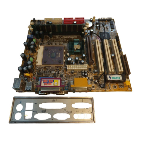
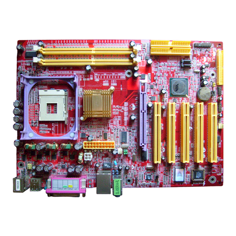
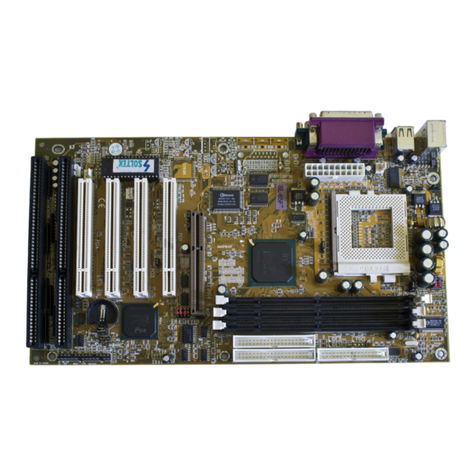
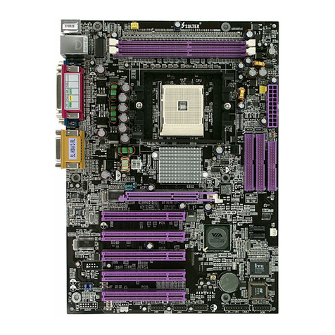
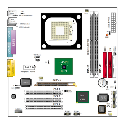
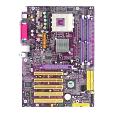
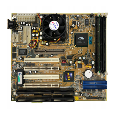
SOLTEK SL-65EB User manual

R
SL-65EB V1.0 USER MANUAL

USER NOTICE
Product Model : SL-65EB
Manual Revision : V1.0
Release Date : O TOBER 2000
His Users Guide & Technical Reference is for assisting system
manufacturers and end-users in setting up and installing the
motherboard.
Every effort has been made to ensure that the information in this
manual is accurate. Solte Computer Inc. is not responsible for print-
ing or clerical errors. Information in this document is subject to
change without notice and does not represent a commitment on the
part of Solte Computer Inc.
No part of this manual may be reproduced, transmitted, translated
into any language in any form or by any means, electronic or
mechanical, including photocopying and recording, for any purpose
without the express written permission of Solte Computer Inc.
Companies and products mentioned in this manual are for identifi-
cation purpose only. Product names appearing in this manual may
or may not be registered trademar s or copyrights of their respec-
tive companies.
Solte computer inc. Provides this manual “As is “ without warranty
of any ind, either express or implied, including but not limited to
the implied warranties or conditions of merchantability or fitness for
a particular purpose. In no event shall Solte computer inc. Be li-
able for any loss or profits, loss of business, loss of use or data,
interruption of business, or for indirect, special, incidental, or con-
sequential damages of any ind, even if Solte computer inc. Has
been advised of the possibility of such damages arising from any
defect or error in this manual or product.
Copyright © 2000 So tek Computer Inc. A Rights Reserved.
• Intel, Celeron, Pentium II, Pentium III are trademar s of Intel Corporation.
• Intel 82815 Graphic Memory Controller Hub(GMCH), 82801 I/O Controller Hub(ICH) are trade-
mar s of Intel Corporation.
• VIA Cyrix III is trademar of VIA Corporation.
• Norton AntiVirus, Norton Ghost are trademar s of Symantec Corporation.
T
SOLTEK AROUND THE WORLD
SOLTEK COMPUTER INC.
Address : 7F, No. 306-3, Ta-Tung Rd, Sec.1, Hsi-Chin, Taipei-
Hsien, Taiwan, R.O.C.
Telephone : 886-2-2642-9060
Fax : 886-2-2642-9065
E-mail : sashia@solte .com.tw
Web site : http://www.solte .com.tw
SOLTEK KOREA INC.
Address : 1002, Chungjin Bldg. 53-5 Wonhyo-Ro, 3-Ka,
Yongsan-Ku Seoul 140-113, Korea
Telephone : 82-2-32717400
Fax : 82-2-32717405
E-mail : solte @nuri.net
MOKA HOLDING B.V.
Address : De Run 4428 5503 LR Veldhoven, the Netherlands
Telephone : 31-402-556150
Fax : 31-402-546006
E-mail : info@mo a.nl
SOUL TECHNOLOGY EUROPE B.V.
Address : Sydneystraat 52-54 3047 BP Rotterdam, the Nether-
lands
Telephone : 31-10-2457492
Fax : 31-10-2457493
E-mail : [email protected]
Web site : http://www.soultech-europe.com

65EB
4
C O N T E N T
CHAPTER 1
INTRODUCTION.................................................................. 6
1-1 ITEM LIST CHECK UP .............................................................................. 6
1-2 CHIPSET ................................................................................................... 6
1-3 PROCESSOR ............................................................................................ 6
1-4 ADVANCED HIGH-PERFORMANCE DRAM CONTROLLER ................... 6
1-5 FULL FEATURED ACCELERATED GRAPHICS PORT ............................ 6
1-6 MULTI-I/O FUNCTION ............................................................................... 7
1-7 EXTENSION SLOTS ................................................................................. 7
1-8 BIOS .......................................................................................................... 7
1-9 POWER MANAGEMENT........................................................................... 7
1-10 FORM FACTOR ....................................................................................... 7
1-11 MOTHERBOARD LAYOUT --- 65EB ....................................................... 8
1-12 CHIPSET SYSTEM BLOCK DIAGRAM................................................... 9
CHAPTER 2
HARDWARE SETUP ......................................................... 11
2-1 CPU INSTALLATION ............................................................................... 11
2-2 MEMORY INSTALLATION ....................................................................... 13
2-3 Hdd / fdd installation ................................................................................ 14
2-4 CPU TYPE CONFIGURATION ................................................................ 15
2-5 SYSTEM MEMORY CONFIGURATION .................................................. 16
2-6 JUMPER DEFINITION ............................................................................. 16
2-6.1 ONBOARD (CFAN1/SFAN1/PFAN1) .................................................... 16
2-6.2 KEYBOARD POWER ON (JP2) ........................................................... 17
2-6.3 USB PORT SELECT (JP6/JP7) ............................................................ 17
2-6.4 POWER LOST RESUME (JP12) .......................................................... 17
2-6.5 VGA CARD (JVGA1) ............................................................................ 18
2-6.6 CLEAR CMOS DATA (JBAT1) .............................................................. 18
2-6.7 WAKE ON LAN (WOL) FUNCTION (JWOL1) ...................................... 18
2-7 CONNECTORS ....................................................................................... 19
2-7.1 J1 SWITCH SIGNAL SUMMARY ......................................................... 20

65EB
5
2-7.2 J2 SWITCH SIGNAL SUMMARY ......................................................... 22
2-7.3 ATX POWER SUPPLY CONNECTOR .................................................. 24
2-7.4 PS/2 MOUSE AND PS/2 KEYBOARD .................................................. 24
2-7.5 IRQ DESCRIPTION .............................................................................. 25
CHAPTER 3
SOFTWARE SETUP .......................................................... 26
3-1 ABOUT THE SUPPORT CD ....................................................... 26
3-2 INTEL CHIPSET DRIVER INSTALLATION (FOR ....................... 26
WINDOWS 95/98/2000) .............................................................. 26
CHAPTER 4
BIOS SETUP ..................................................................... 28
4-1 INTRODUCE THE BIOS .......................................................................... 28
4-2 WHAT IS BIOS SETUP............................................................................ 28
4-3 HOW TO RUN BIOS SETUP ................................................................... 28
4-4 WHAT IS CMOS ...................................................................................... 29
4-5 WHAT IS POST ....................................................................................... 29
4-6 BIOS UPGRADE...................................................................................... 29
4-6.1 BEFORE UPGRADE BIOS ................................................................... 29
4-6.2 UPGRADE PROCESS ......................................................................... 30
4-7 CMOS SETUP UTILITY ........................................................................... 33
4-8 STANDARD CMOS FEATURES .............................................................. 34
4-9 ADVANCED BIOS FEATURES ................................................................ 37
4-10 ADVANCED CHIPSET FEATURES ....................................................... 41
4-11 INTEGRATED PERIPHERALS .............................................................. 45
4-12 POWER MANAGEMENT SETUP.......................................................... 50
4-13 PNP / PCI CONFIGURATION ................................................................ 55
4-14 FREQUENCY CONTROL ...................................................................... 58
4-15 LOAD OPTIMIZED DEFAULTS ............................................................. 58
4-16 SET SUPERVISOR / USER PASSWORD ............................................. 60
4-17 SAVE & EXIT SETUP ............................................................................ 61
4-18 EXIT WITHOUT SAVING ....................................................................... 61

65EB
6
CHAPTER 1
INTRODUCTION
1-1 ITEM LIST CHECK UP
• Motherboard
• Support CD
• User’s Manual
• Bundle Bonus Pac CD
• Bundle Bonus Pac Manual
• ATA33 IDE Cable
1-2 CHIPSET
• North Bridge - Intel 82443BX.
• South Bridge - 82371EB PCI-To-ISA.
• Supper I/O - Winbond W83977.
1-3 PROCESSOR
• Supports Intel® FC-PGA Pentium IIITM up to 1GHz (100MHz Front Side
Bus on y).
• Supports Intel® FC-PGA 370 Celeron & PGA 370 Celeron up to 700MHz.
• Supports VIA Cyrix III up to 600MHz.
• Supports CPU voltage Auto - Detect circuit.
• Supports CPU using front side Bus 66MHz and 100MHz only.
1-4 ADVANCED HIGH-PERFORMANCE DRAM
CONTROLLER
• Supports SDRAM memory up to 3 DIMMS.
• 64-bit data width and 3.3V DRAM interface.
• Supports up to 768MB memory space.
• Different DRAM types may be used in mixed combinations.
1-5 FULL FEATURED ACCELERATED GRAPHICS PORT
• Supports 66MHz 1x and 2x modes.
• AGP Specification Rev 1.0 compliant.

65EB
7
1-6 MULTI-I/O FUNCTION
• Two UltraDMA-33 Master Mode PCI EIDE ports.
• Two UARTs for Complete Serial Ports.
• One dedicated IR connector:
Third serial port dedicated to IR function either through the two complete serial ports or the
third dedicated port Infrared-IrDA (SIR) and ASK (Amplitude Shift Keyed) IR.
• Multi-mode parallel connector:
Standard mode, ECP and EPP support.
• Floppy Dis connector:
One FDD with drive swap support.
• Universal Serial Bus connector:
USB V1.0 compatible.
Provides 2 build-in USB ports.
• PS/2 Keyboard connector.
• PS/2 Mouse connector.
1-7 EXTENSION SLOTS
• Five PCI bus Mater slots.
• Three DIMM slots.
• One ISA slot.
• One AGP 2X mode slot.
1-8 BIOS
• Award BIOS V6.0.
• Supports Plug & Play V1.0.
• Flash Memory for easy upgrade.
• Year 2000 compliant.
1-9 POWER MANAGEMENT
• ACPI 1.0 compliant (Advanced Configuration and Power Interface).
• APM V1.2 compliant (Legacy power management).
• System event monitoring with two event classes.
• Supports PS/2 Keyboard & Mouse power on.
• Supports Wa e On LAN (WOL) & Wa e On Modem.
• Supports real time cloc (RTC) with date alarm, month alarm, and century field.
1-10 FORM FACTOR
• ATX from factor, 4 layers PCB.
• Motherboard size 18.0cm x 30.5cm.

65EB
8
NOTE: FOR 100 / 133MHz CPU ENVIRONMENT, THE SDRAM MUST COMPLY WITH PC-100 / PC-
133 SPEC.
1-11 MOTHERBOARD LAYOUT --- 65EB
• DEFAULT SETTING: Celeron 300/66MHz.
3
1
JP2
1 3
1 3
JVGA1
JP6
JP7
1 3
JP12
1 3
JBAT1
CFAN1
SFAN1
PFAN1
SPK RST PWR/LED SUSLED
HD/LED IR PWR SMI
J1
J2
15
15
JWOL1
AGP
PCI 1
PCI 2
PCI 3
PCI 4
PCI 5
FDC
DIMM1
DIMM2
DIMM3
IDE2
IDE1
SOCKET 370
ATX POWER
ISA
FLASH BIOS
Li
Battery
C ock
Generator
I/O
Contro er
82443BX
Host
Bridge
82371EB
(PIIX4E)
(PCI-to-ISA
Bridge)
USB0
USB1 PS/2
MOUSE
PS/2
K/B
LPT1
COM2 COM1
upper
lower
upper
lower
SW1
ONDIP
8 7 6 5 4 3 2 1
PC100/PC133 SDRAM

65EB
9
1-12 CHIPSET SYSTEM BLOCK DIAGRAM
82443BX
Host
Bridge
82371EB
(PIIX4E)
(PCI-to-ISA
Bridge)
ISA1
Keyboard
& Mouse
Main
Memory
(DRAM)
AGP S ot or
3D Graphics
Contro er
BIOS
ROM
IDE x 2 Ports
(U tra DMA/33)
USBx2
Super O
Seria Port x 2
Infrared Port x 1
Para e Port x 1
FDD x1
Socket 370
CPU
PCI3
PCI5
PCI4
PCI1
PCI2
Figure 1-11. 82443BX System B ock Diagram Using the
82371EB South Bridge
AGP 2X S ot

65EB
10
ATTENTION !!!
1. P ease refer to your processor insta ation or other
documentation attached with your CPU for detai ed
insta ing instruction.
2. Insta ing a heat sink and coo ing fan is necessary for
proper heat dissipation from your CPU. Uncorrected
insta ation may resu t in overheating and damage of
your CPU.
3. Before changing the setting of CPU Vcore from BIOS
program, user SHOULD make sure of correct specifi-
cation both of CPU CLOCK and RATIO. Uncorrected
setting may cause damage to your CPU.

65EB
11
SOCKET 370
2-1 CPU INSTALLATION
WARNING ! Never run you processor without the heat sin properly and
firmly attached. PERMANET DAMAGE WILL RESULT!
1. Pull the lever sideways away from the soc et, and then raise the lever up
to a 90-degree angle.
2. Ta e note of the red circle as below picture. When insert the CPU into
soc et, you can find out there is a definite pin orientation for CPU and
soc et.
SOCKET 370
CHAPTER 2
HARDWARE SETUP

65EB
12
3. Ma e sure that the CPU positions in the soc et tightly, and then put the
lever down to complete the CPU installation.
SOCKET 370

65EB
13
168-Pin DIMM Notch Key Definitions(3.3V)
DRAM Key Position Vo tage Key Position
Unbuffered 3.3V
2-2 MEMORY INSTALLATION
WARING!
• Ma e sure that you unplug your power supply when adding or removing
memory modules or other system components, failure to do so may cause
severe damage to both your motherboard and expansion cards.
• Be careful when inserting or removing DIMM, forcing a DIMM in or out of a
soc et can be damaged the memory module or the soc et. Some of DIMMs
contain EDO or FTP DRAM that accept only 5V power. These DIMM types
are incompliant with the motherboard, the M/B only supports 3.3V true SDRAM
DIMMs
Removing:
• Press the holding clips on both sides of soc et out ward to release the DIMM,
Gently pull the DIMM out of the soc et.
Insta ing DIMM:
• Ma e sure you have the correct memory module type for your motherboard.
• Insert the module(s) as shown, DIMMs have 168-pins and two notches that
will match with the onboard DIMM soc et, memory modules are installed by
inserting them straight into the slot until they “clic ” into place. They only fit in
one direction so do not force them into place.

65EB
14
3
1
JP2
1 3
1 3
JVGA1
JP6
JP7
1 3
JP12
1 3
JBAT1
CFAN1
SFAN1
PFAN1
SPK RST PWR/LED SUSLED
HD/LED IR PWR SMI
J1
J2
15
15
JWOL1
AGP
PCI 1
PCI 2
PCI 3
PCI 4
PCI 5
FDC
DIMM1
DIMM2
DIMM3
IDE2
IDE1
SOCKET 370
ATX POWER
ISA
FLASH BIOS
Li
Battery
C ock
Generator
I/O
Contro er
82443BX
Host
Bridge
82371EB
(PIIX4E)
(PCI-to-ISA
Bridge)
USB0
USB1 PS/2
MOUSE
PS/2
K/B
LPT1
COM2 COM1
upper
lower
upper
lower
SW1
ONDIP
8 7 6 5 4 3 2 1
PC100/PC133 SDRAM
2-3 HDD / FDD INSTALLATION
• you must configure the second drive to Slave mode by setting its jumper
accordingly.Please refer to your hard dis documentation for the jumper
settings.
• To install FDD (Floppy Dis Drive), you may connect the single end to the
board , and connect two plugs on the other end to the floopy drives.
Floppy Disk Drive
Connector:
Orient the red markings
on the floppy ribbon
cable to Pin1.
Hard Disk Drive
Connector:
Orient the red markings
on the ID ribbon cable
to Pin1.
• Even though the IDE controller on the Motherboard supports Ultra ATA33
only, but it also compatible with ultra ATA66, ATA100 and legacy IDE devise.

65EB
15
2-4 CPU TYPE CONFIGURATION
2-4.2 BUS CLOCK SELECT
2-4.1 BUS RATIO SELECT
SW1 DIP1 ~ DIP4 SETTING
3.0x 3.5x
4.0x 4.5x
5.0x 5.5x
6.0x 6.5x
7.0x 7.5x
8.0x
ON
ON
ON
ON
12345678
OFF
ON
ON
ON
12345678
OFF
OFF
ON
ON
ON
ON
12345678
OFF
ON
ON
ON
12345678
OFF
OFF
ON
ON
ON
12345678
OFF
OFF
ON
ON
12345678
OFF
OFF
OFF
ON
ON
ON
ON
12345678
OFF
ON
ON
ON
12345678
OFF
OFF
ON
ON
ON
12345678
OFF
OFF
ON
ON
12345678
OFF
OFF
OFF
ON
ON
ON
12345678
OFF
OFF
• Normally, the Bus Ratio (Frenquency Multiple) of your processor is loc ed
by processor’s Vendor,setting of the CPU Bus Ratio will have no effect.
• Bus Ratio exceed 8.0X, user can not change all values from DIP switch,
the Bus ratio will be detected by BIOS automatically.
• The Bus Ratio Setting is available on unloc ed processors only.
• Over cloc ing is not recommended, your system may wor unstable.
Auto Se ect 66/100 MHz
(defau t)
SW1 DIP5 ~ DIP8 SETTING
66MHz
100MHz
ON
ON
ON
87654321
OFF
OFF
ON
ON
87654321
OFF
OFF
OFF
ON
ON
ON
87654321
OFF
OFF

65EB
16
2-5 SYSTEM MEMORY CONFIGURATION
• This Intel 82443BX motherboard supports 168pin DIMM of 32MB, 64MB,
128MB, and 256MB to form a memory size between 32MB up to 768MB
(SDRAM). Intel 82443BX chipset provides “Table-Free” function. It means
that users can install DRAM with any configuration and in any ban , and
that is why the DRAM table is not needed but do remember that the DRAM
must be 3.3V type. For 100 MHz CPU environment, the SDRAM specifi-
cation must comp y with PC-100 / PC-133 spec.
2-6 JUMPER DEFINITION
• The figure below shows the location of the motherboard’s jumper bloc s.
CAUTION
• Do not move the jumper with the power on. Always turn off the power and unplug
the power cord from the computer before changing the jumper. Otherwise, the
motherboard could be damaged.
Those connectors support processor/system/chassis cooling fan with
+12V. Those support three pin head connector. When connecting the wire
to FAN connectors, user should give attention that the red wire is the
positive and should be connected to the +12V, the black wire is Ground
and should be connected to GND. If your motherboard has Hardware
Monitor chipset on-board, you must use a specially designed fan with
speed sensor to take advantage of this function.
For fans with fan speed sensor, every rotation of the fan will send out
2 pulses. System Hardware Monitor will count and report the fan rotation
speed.
CPU FAN
CFAN1/SFAN1/PFAN1: ONBOARD FAN (12V)
SFAN1
CFAN1
CHASSIS FAN PFAN1
SYSTEM FAN
2-6.1 ONBOARD (CFAN1/SFAN1/PFAN1)

65EB
17
GND
+12V
SENSOR
NOTE 1: Always consult vendor for proper PU cooling fan.
NOTE 2: PU FAN supports the FAN control. You can install P
Alert utility. This will automatically control the PU FAN
speed according to the actual PU temperature.
Enabled
Normal (default)
JP12: POWER LOST RESUME
1 3
JP12
1 3
JP12
NOTE: This jumper allows user to use the switch of ATX power supply
to control ON/OFF switch directly instead of using the power
switch on the motherboard.
2-6.4 POWER LOST RESUME (JP12)
2-6.2 KEYBOARD POWER ON (JP2)
NOTE: This function allows you to use PS/2 keyboard or PS/2 mouse
to power on your system, the function must be set in junction
with “Power on function” state in BIOS setup “Integrated
peripherals” section.
Disabled (default)
Enabled
JP2: KEYBOARD POWER ON
JP2
3
1
3
1
JP2
Redirect USB port to USB 1
connector (default)
JP6/JP7: USB PORT SELECT
1 3
1 3
JP6
JP7
1 3
1 3
JP6
JP7
Redirect USB port to AGP
2-6.3 USB PORT SELECT (JP6/JP7)

65EB
18
2-6.5 VGA CARD (JVGA1)
For PCI VGA Card
Normal (default)
JVGA1 : VGA CARD
JVGA1
JVGA1
NOTE: This jumper is set for the P I VGA ard only. Open this
jumper when the system is not able to boot up. If you use
AGP ard, it is important to leave “JVGA1” at default setting.
2-6.6 CLEAR CMOS DATA (JBAT1)
NOTE: We recommend user to unplug the power cord from ATX
power supply to take precautions. lear MOS memory by
shorting this jumper pin 2 & pin3 momentarily, and then
remove the cap back to pin 1 & pin2 to retain original MOS
setting.
Clear CMOS Data
Retain Data (default)
JBAT1: CLEAR CMOS DATA
3
1
JBAT1
3
1
JBAT1
This connector connects to a LAN card with a Wake On LAN output.
The connector powers up the system when a wake-up packet or signal is
received through the LAN card.
This feature requires that Wake On LAN feature is enabled at the
BIOS “Power Management Setup” and that your system has an ATX
power supply with at least 720mA / +5V standby power.
Connect the Wa e On LAN signal from LAN card ¤
to JWOL1
JWOL1 : WAKE ON LAN (WOL) FUNCTION
JWOL1
GND
+5V standby
PME
2-6.7 WAKE ON LAN (WOL) FUNCTION (JWOL1)

65EB
19
A : PS/2 MOUSE
B : USB O
C : LPT 1
D : PS/2 KEYBOARD
E : USB 1
F : COM 1
G : COM 2
A.
D. E. F. G.
B. C.
2-7 CONNECTORS
A1 : 1st HDD LED
A2 : 2nd HDD LED
B : INFRARED (IR)
C : POWER SWITCH
D : SMI
E : SPEAKER
F : RESET SWITCH
G : POWER LED
H : KEYLOCK
I : SUSPEND LED
EF G
C
H I
D
A1 A2 B
++
--
+-
J1
J2
1 15
1 15

65EB
20
2-7.1 J1 SWITCH SIGNAL SUMMARY
123456789101112131415
J2
J1
PIN 1 +5V
HDD LED CONNECTOR
PIN 2 HDD LED SIGNAL
PIN 3 HDD LED SIGNAL
PIN 4 +5V
DESCRIPTION
This connector supp ies power to the cabinet's IDE
activity LED. Read and write activity by devices
connected to the Primary or SecondaryIDE
connector wi cause the LED to ight up.
123456789101112131415
J2
J1
INFRARED CONNECTOR
PIN 6 INFRARED TRANSMIT SIGNAL
PIN 7 GND
PIN 8 INFRARED RECEIVE SIGNAL
PIN 9 NONE
PIN 10 +5V
DESCRIPTION
This connector supports an optiona wire ess
transmitting and receiving infrared modu e. This
modu e mounts to a sma opening on system cases
that support this feature.
User must a so configure the setting through
BIOS program "Periphera Setup" to se ect whether
UART2 is directed for use with COM2 or IrDA.
Use the five pins and connect a ribbon cab e from
the modu e to the motherboard's IR connector
according to the pin definitions.
Table of contents
Other SOLTEK Motherboard manuals

SOLTEK
SOLTEK SL-65ME User manual

SOLTEK
SOLTEK SL-B8D-F User manual

SOLTEK
SOLTEK SL-63AV User manual

SOLTEK
SOLTEK NV400-64 User manual

SOLTEK
SOLTEK SL-63AV Use and care manual

SOLTEK
SOLTEK SL-PM800I User manual

SOLTEK
SOLTEK SL-56H5 User manual

SOLTEK
SOLTEK SL-65EP+-T User manual

SOLTEK
SOLTEK SL-75DRV-X User manual

SOLTEK
SOLTEK SL-75MIV User manual

SOLTEK
SOLTEK SL-85DR-C User manual

SOLTEK
SOLTEK 75FRN2 Series User manual

SOLTEK
SOLTEK SL-85MR2 User manual

SOLTEK
SOLTEK B9A-FGR User manual

SOLTEK
SOLTEK SL-85LIR3 User manual

SOLTEK
SOLTEK SL-54A2 User manual

SOLTEK
SOLTEK SL-65KVB User manual

SOLTEK
SOLTEK SL-85DRV+ User manual

SOLTEK
SOLTEK 85DRV4-C User manual

SOLTEK
SOLTEK SL-85ERV4-R User manual