Spectrum Digital TMS320VC5509A EVM PLUS Use and care manual

TMS320VC5509A EVM PLUS
2004 DSP Development Systems
Reference
Technical


TMS320VC5509A EVM PLUS
Technical Reference
507755-0001 Rev. A
October 2004
SPECTRUM DIGITAL, INC.
12502 Exchange Drive, Suite 440 Stafford, TX. 77477
Tel: 281.494.4505 Fax: 281.494.5310

IMPORTANT NOTICE
Spectrum Digital, Inc. reserves the right to make changes to its products or to discontinue any
product or service without notice. Customers are advised to obtain the latest version of relevant
information to verify that the data being relied on is current before placing orders.
Spectrum Digital, Inc. warrants performance of its products and related software to current
specifications in accordance with Spectrum Digital’s standard warranty. Testing and other quality
control techniques are utilized to the extent deemed necessary to support this warranty.
Please be aware that the products described herein are not intended for use in life-support
appliances, devices, or systems. Spectrum Digital does not warrant nor is Spectrum Digital liable for
the product described herein to be used in other than a development environment.
Spectrum Digital, Inc. assumes no liability for applications assistance, customer product design,
software performance, or infringement of patents or services described herein. Nor does Spectrum
Digital warrant or represent any license, either express or implied, is granted under any patent right,
copyright, or other intellectual property right of Spectrum Digital, Inc. covering or relating to any
combination, machine, or process in which such Digital Signal Processing development products or
services might be or are used.
WARNING
This equipment is intended for use in a laboratory test environment only. It generates, uses, and can
radiate radio frequency energy and has not been tested for compliance with the limits of computing
devices pursuant to subpart J of part 15 of FCC rules, which are designed to provide reasonable
protection against radio frequency interference. Operation of this equipment in other environments
may cause interference with radio communications, in which case the user at his own expense will be
required to take whatever measures necessary to correct this interference.
Copyright © 2004 Spectrum Digital, Inc.

Contents
1 Introduction to the TMS320VC5509A EVM PLUS Module . . . . . . . . . . . . . . . . . . . . . . . . 1-1
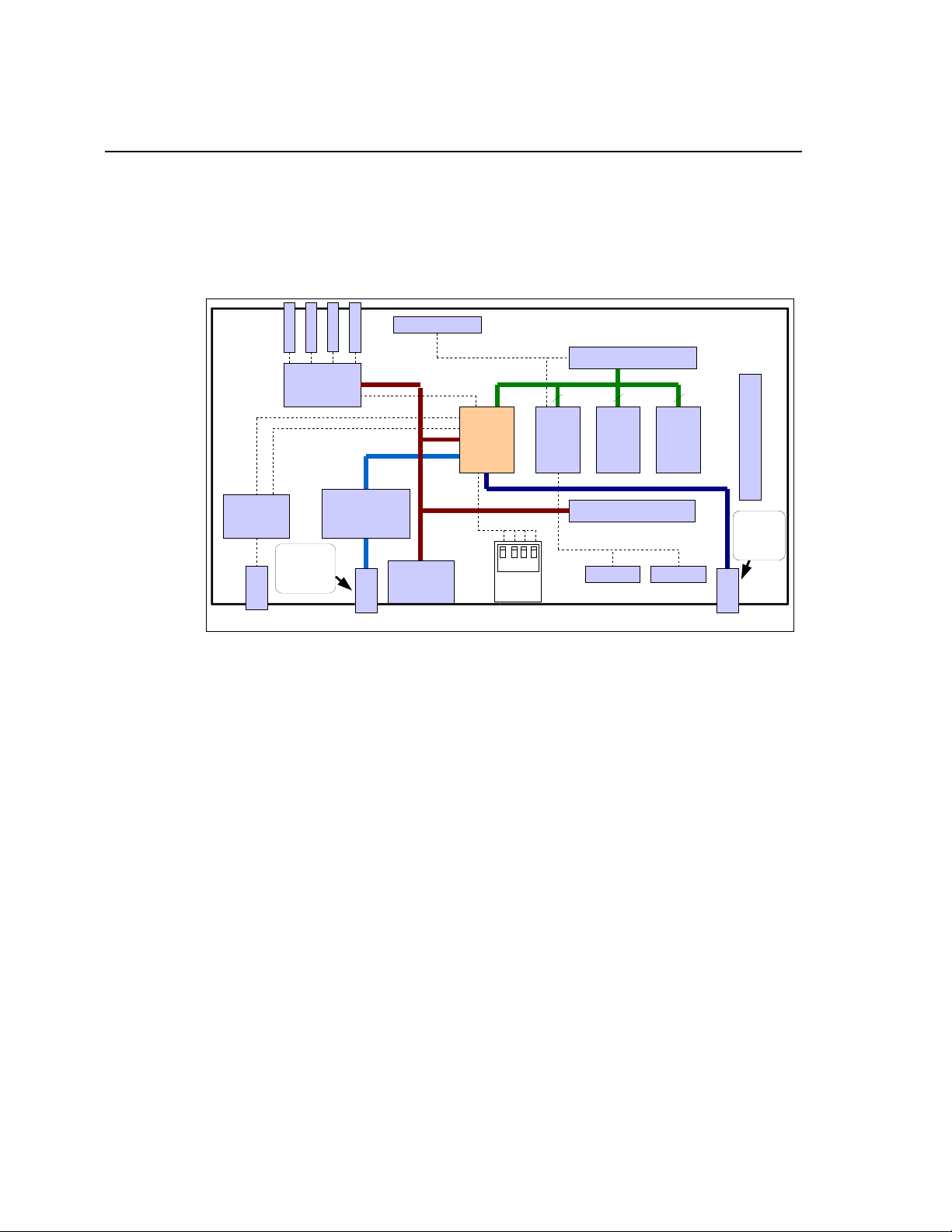
Provides you with a description of the TMS320VC5509A EVM PLUS Module, key features, and
block diagram.
1.1 Key Features . . . . . . . . . . . . . . . . . . . . . . . . . . . . . . . . . . . . . . . . . . . . . . . . . . . . . . . . . . 1-2
1.2 Functional Overview . . . . . . . . . . . . . . . . . . . . . . . . . . . . . . . . . . . . . . . . . . . . . . . . . . . . 1-3
1.3 Basic Operation . . . . . . . . . . . . . . . . . . . . . . . . . . . . . . . . . . . . . . . . . . . . . . . . . . . . . . . . . 1-4
1.4 Memory Map . . . . . . . . . . . . . . . . . . . . . . . . . . . . . . . . . . . . . . . . . . . . . . . . . . . . . . . . . . 1-5
1.5 Boot Mode Settings . . . . . . . . . . . . . . . . . . . . . . . . . . . . . . . . . . . . . . . . . . . . . . . . . . . . . 1-6
1.6 Power Supply . . . . . . . . . . . . . . . . . . . . . . . . . . . . . . . . . . . . . . . . . . . . . . . . . . . . . . . . . 1-8
2 Board Components . . . . . . . . . . . . . . . . . . . . . . . . . . . . . . . . . . . . . . . . . . . . . . . . . . . . . . . . 2-1
Describes the operation of the major board components on the TMS320VC5509A EVM PLUS.
2.1 CPLD (programmable Logic) . . . . . . . . . . . . . . . . . . . . . . . . . . . . . . . . . . . . . . . . . . . 2-2
2.1.1 CPLD Overview . . . . . . . . . . . . . . . . . . . . . . . . . . . . . . . . . . . . . . . . . . . . . . . . . . . . 2-2
2.1.2 CPLD Registers . . . . . . . . . . . . . . . . . . . . . . . . . . . . . . . . . . . . . . . . . . . . . . . . . . . . . 2-3
2.1.3 USER_REG Register . . . . . . . . . . . . . . . . . . . . . . . . . . . . . . . . . . . . . . . . . . . . . . 2-4
2.1.4 DC_REG Register . . . . . . . . . . . . . . . . . . . . . . . . . . . . . . . . . . . . . . . . . . . . . . . . . . 2-4
2.1.5 Version Register . . . . . . . . . . . . . . . . . . . . . . . . . . . . . . . . . . . . . . . . . . . . . . . . . . 2-5
2.1.6 MISC Register . . . . . . . . . . . . . . . . . . . . . . . . . . . . . . . . . . . . . . . . . . . . . . . . . . . . . 2-5
2.1.7 Interrupt Register . . . . . . . . . . . . . . . . . . . . . . . . . . . . . . . . . . . . . . . . . . . . . . . . . . . 2-6
2.1.8 LCD0 Address0 Register . . . . . . . . . . . . . . . . . . . . . . . . . . . . . . . . . . . . . . . . . . . 2-7
2.2 AIC23 Codec . . . . . . . . . . . . . . . . . . . . . . . . . . . . . . . . . . . . . . . . . . . . . . . . . . . . . . 2-8
2.3 Sychronous DRAM . . . . . . . . . . . . . . . . . . . . . . . . . . . . . . . . . . . . . . . . . . . . . . . . . 2-9
2.4 Flash Memory . . . . . . . . . . . . . . . . . . . . . . . . . . . . . . . . . . . . . . . . . . . . . . . . . . . . 2-9
2.5 LEDs and DIP Switches . . . . . . . . . . . . . . . . . . . . . . . . . . . . . . . . . . . . . . . . . . . . . 2-9
2.6 Core Power Control . . . . . . . . . . . . . . . . . . . . . . . . . . . . . . . . . . . . . . . . . . . . . . . . 2-10
2.7 Current Shunts . . . . . . . . . . . . . . . . . . . . . . . . . . . . . . . . . . . . . . . . . . . . . . . . . . . . 2-10
2.8 MMC Interface . . . . . . . . . . . . . . . . . . . . . . . . . . . . . . . . . . . . . . . . . . . . . . . . . . . . 2-11
2.9 LCD Display/Keyboard Interface . . . . . . . . . . . . . . . . . . . . . . . . . . . . . . . . . . . . . . 2-11
2.10 Daughter Card Interface . . . . . . . . . . . . . . . . . . . . . . . . . . . . . . . . . . . . . . . . . . . . . 2-12
3 Physical Specifications . . . . . . . . . . . . . . . . . . . . . . . . . . . . . . . . . . . . . . . . . . . . . . . . . . . . 3-1
Describes the physical layout of the TMS320VC5509A EVM PLUS and its connectors.
3.1 Board Layout . . . . . . . . . . . . . . . . . . . . . . . . . . . . . . . . . . . . . . . . . . . . . . . . . . . . . . . . 3-2
3.2 Connector Index . . . . . . . . . . . . . . . . . . . . . . . . . . . . . . . . . . . . . . . . . . . . . . . . . . . . 3-3
3.3 Expansion Connectors . . . . . . . . . . . . . . . . . . . . . . . . . . . . . . . . . . . . . . . . . . . . . . . . 3-3
3.3.1 P1, Memory Expansion . . . . . . . . . . . . . . . . . . . . . . . . . . . . . . . . . . . . . . . . . . . . . 3-4
3.3.2 P2, Peripheral Expansion . . . . . . . . . . . . . . . . . . . . . . . . . . . . . . . . . . . . . . . . . . . . 3-5
3.3.3 P3, National Instruments Interface . . . . . . . . . . . . . . . . . . . . . . . . . . . . . . . . . . . . 3-6
3.3.3.1 Analog Probe Connector . . . . . . . . . . . . . . . . . . . . . . . . . . . . . . . . . . . . . . . . . 3-7
3.3.3.2 National Instruments Protype Header . . . . . . . . . . . . . . . . . . . . . . . . . . . . . . . . 3-7
3.3.5 J11, Keypad/display Interface . . . . . . . . . . . . . . . . . . . . . . . . . . . . . . . . . . . . . . . 3-8

3.3.6 J12, SD/MMC Interface . . . . . . . . . . . . . . . . . . . . . . . . . . . . . . . . . . . . . . . . . . . . . 3-8
3.4 Audio Connectors . . . . . . . . . . . . . . . . . . . . . . . . . . . . . . . . . . . . . . . . . . . . . . . . . . . . . 3-9
3.4.1 J301, Microphone Connector . . . . . . . . . . . . . . . . . . . . . . . . . . . . . . . . . . . . . . . . . 3-9
3.4.2 J303, Audio Line In Connector . . . . . . . . . . . . . . . . . . . . . . . . . . . . . . . . . . . . . . . . 3-9
3.4.3 J304, Audio Line Out Connector . . . . . . . . . . . . . . . . . . . . . . . . . . . . . . . . . . . . . . 3-10
3.4.4 J302, Headphone Connector . . . . . . . . . . . . . . . . . . . . . . . . . . . . . . . . . . . . . . . . . 3-10
3.5 Power Connectors . . . . . . . . . . . . . . . . . . . . . . . . . . . . . . . . . . . . . . . . . . . . . . . . . . . . 3-11
3.5.1 J5, +5V Main Power Connector . . . . . . . . . . . . . . . . . . . . . . . . . . . . . . . . . . . . . . 3-11
3.5.2 J6, Optional Power Connector . . . . . . . . . . . . . . . . . . . . . . . . . . . . . . . . . . . . . . . . 3-11
3.6. Miscellaneous Connectors . . . . . . . . . . . . . . . . . . . . . . . . . . . . . . . . . . . . . . . . . . . 3-12
3.6.1 J201, USB Port . . . . . . . . . . . . . . . . . . . . . . . . . . . . . . . . . . . . . . . . . . . . . . . . . . . . 3-12
3.6.2 J7, External JTAG Connector . . . . . . . . . . . . . . . . . . . . . . . . . . . . . . . . . . . . . . . . . . 3-12
3.6.3 JP1, PLD Programming Connector . . . . . . . . . . . . . . . . . . . . . . . . . . . . . . . . . . . . . 3-13
3.7 User LEDs . . . . . . . . . . . . . . . . . . . . . . . . . . . . . . . . . . . . . . . . . . . . . . . . . . . . . . . . . 3-13
3.8 System LEDs . . . . . . . . . . . . . . . . . . . . . . . . . . . . . . . . . . . . . . . . . . . . . . . . . . . . . . . 3-13
3.9 User DIP Switch . . . . . . . . . . . . . . . . . . . . . . . . . . . . . . . . . . . . . . . . . . . . . . . . . . . . 3-13
3.10 Reset Switch . . . . . . . . . . . . . . . . . . . . . . . . . . . . . . . . . . . . . . . . . . . . . . . . . . . . . . . 3-14
3.11 Wake Up Switch . . . . . . . . . . . . . . . . . . . . . . . . . . . . . . . . . . . . . . . . . . . . . . . . . . . 3-14
3.12 Test Points . . . . . . . . . . . . . . . . . . . . . . . . . . . . . . . . . . . . . . . . . . . . . . . . . . . . . . . . 3-15
A Schematics . . . . . . . . . . . . . . . . . . . . . . . . . . . . . . . . . . . . . . . . . . . . . . . . . . . . . . . . . . . . . . A-1
Contains the schematics for the TMS320VC5509A EVM PLUS
B Mechanical Information . . . . . . . . . . . . . . . . . . . . . . . . . . . . . . . . . . . . . . . . . . . . . . . . . . B-1
Contains the mechanical information about the TMS320VC5509A EVM PLUS

About This Manual
This document describes the board level operations of the TMS320VC5509A
Evaluation Module (EVM PLUS). The EVM PLUS is based on the Texas Instruments
TMS320VC5509A Digital Signal Processor.
The TMS320VC5509A EVM PLUS is a table top card to allow engineers and software
developers to evaluate certain characteristics of the TMS320VC5509A DSP to
determine if the processor meets the designers application requirements. Evaluators
can create software to execute on board or expand the system in a variety of ways.
Notational Conventions
This document uses the following conventions.
The TMS320VC5509A will sometimes be referred to as the C55XX.
The TMS320VC5509A EVM PLUS will sometimes be referred to as the EVM PLUS.
Program listings, program examples, and interactive displays are shown is a special
italic typeface. Here is a sample program listing.
equations
!rd = !strobe&rw;
Information About Cautions
This book may contain cautions.
This is an example of a caution statement.
A caution statement describes a situation that could potentially damage your software,
or hardware, or other equipment. The information in a caution is provided for your
protection. Please read each caution carefully.
Related Documents
Texas Instruments TMS320VC55XX DSP CPU Reference Guide
Texas Instruments TMS320VC55XX DSP Peripherals Reference Guide

Table 1: Hardware History
Revision History
A Alpha Release
Table 2: Manual History
Revision History
A Alpha Release

1-1
Chapter 1
Introduction to the
TMS320VC5509A EVM PLUS
Chapter One provides a description of the TMS320VC5509A EVM PLUS
along with the key features and a block diagram of the circuit board.
Topic Page
1.1 Key Features 1-2
1.2 Functional Overview 1-3
1.3 Basic Operation 1-4
1.4 Memory Map 1-5
1.5 Boot Mode Settings 1-6
1.6 Power Supply 1-8

Spectrum Digital, Inc
1-2 TMS320VC5509A EVM PLUS Technical Reference
1.0 Key Features
The 5509A EVM PLUS is a low-cost standalone development platform that enables
users to evaluate and develop applications for the TI C55XX DSP family. The EVM
PLUS also serves as a hardware reference design for the TMS320VC5509A DSP.
Schematics, logic equations and application notes are available to ease hardware
development and reduce time to market.
The EVM PLUS comes with a full compliment of on-board devices that suit a wide
variety of application environments. Key features include:
• A Texas Instruments TMS320VC5509A-GHH DSP
• Selectable core voltages (1.2V, 1.4V, 1.6V)
• Power test points and current shunts
• An AIC23B stereo codec
• 8 Mbytes of synchronous DRAM
• 512 Kbytes of non-volatile Flash memory
• 4 user accessible LEDs and DIP switches
• User USB port via VC5509A
• Software board configuration through registers implemented in CPLD
• Switch selectable boot options
Figure 1-1, Block Diagram VC5509A EVM PLUS
MMC
JTAG
SDRAM
AIC23
Codec
NI DAQ
Flash
MIC IN
LINE OUT
HPOUT
LINE IN
Peripheral Exp
LED DIP
EMIF
McBSPs
0 1 2 3
0 1 2 3
CPLD
Memory Exp
Voltage
Reg
PWR
USB
Embedded
JTAG
5V
1.6V
3.3V 5509A
DSP
1616 16
LCDDisplay
USB
I2C
5509A
on-chip
USB
5509A
on-chip
USB
Code
Composer
Debug
12
GPIO0
GPIO1
GPIO2
GPIO3
S3
34

Spectrum Digital, Inc
1-3
• 128 x 64 display and position keypad
• Standard expansion connectors for daughter card use
• National Instruments interface
• JTAG emulation through on-board JTAG emulator with USB host
interface or external emulator
• MMC card interface
• Single voltage power supply (+5V)
1.2 Functional Overview of the TMS320VC5509A EVM PLUS
The DSP interfaces to external SDRAM, Flash memory and an expansion memory
interface connector through its 16-bit External Memory Interface (EMIF). The SDRAM
accesses are in 16-bit mode in chip enable 0 memory space. The EMIF provides the
necessary refresh signals. The Flash accesses are in 16-bit asynchronous mode in the
bottom half of chip enable 1 space. The EMIF signals are brought out to the
daughter card expansion connectors which use chip enables 2 and 3.
An on-board AIC23B codec allows the DSP to transmit and receive analog signals.
I2C is used for the codec control interface and McBSP0 is used for data. Analog
I/O is done through four 3.5mm audio jacks that correspond to microphone input, line
input, line output and headphone output. The codec can select the microphone or the
line input as the active input. The analog output is driven to both the line out (fixed
gain) and headphone (adjustable gain) connectors.
McBSP2 interfaces to a MultiMedia card. This allows the DSP a way to store off data
for video and audio applications. McBSP1 and McBSP2 are routed to the expansion
connectors via software configuration registers in the CPLD
A programmable logic device called a CPLD is used to implement glue logic that ties
the board components together. The CPLD has a register based user interface that
lets the user configure the board by reading and writing to the CPLD registers. The
registers reside in the upper half of chip enable 1.
The EVM PLUS includes 4 LEDs and 4 position DIP switch as a simple way to provide
the user with interactive feedback. Both are accessed by reading and writing to the
CPLD registers. A wake-up push button allows the DSP to be interrupted, to “wake up”
the DSP when it is in sleep or idle mode.
An included 5V external power supply is used to power the board. On-board voltage
regulators provide the 1.6V to 1.2V DSP core voltage, 3.3V digital and 3.3V analog
voltages. A voltage supervisor monitors the internally generated voltage, and will hold
the board in reset until the supplies are within operating specifications and the reset
button is released.

Spectrum Digital, Inc
1-4 TMS320VC5509A EVM PLUS Technical Reference
Code Composer communicates with the EVM PLUS through an embedded JTAG
emulator with a USB host interface. The EVM PLUS can also be used with an external
emulator through the external JTAG connector.
1.3 Basic Operation
The EVM PLUS is designed to work with TI’s Code Composer Studio (CCS)
development environment. Code Composer communicates with the board through the
on-board JTAG emulator, or an external emulator. To start, follow the instructions in the
Quick Start Guide to install Code Composer. This process will install all of the
necessary development tools, documentation and drivers.
After the install is complete, follow these steps to run Code Composer. The EVM PLUS
must be fully connected to launch Code Composer Studio.
1) Connect the included power supply to the EVM PLUS.
2) Connect the EVM PLUS to your PC with a mini USB cable (also included).
3) Set up Code Composer Studio
4) Launch Code Composer from its icon on your desktop.
Detailed information about the CCS including a tutorial, examples and reference
material is available in the EVM PLUS’s help file. You can access the help file through
Code Composer’s help menu.

Spectrum Digital, Inc
1-5
1.4 Memory Map
The C55x family of DSPs has a unified program and data space with a separate distinct
I/O space dedicated to on-chip peripheral registers. For a number of reasons
(historical and technical) though, program code is addressable in 8-bit bytes while data
is addressable in 16-bit words. Both programs and data can reside anywhere in the
unified memory space.
The address reach of the 5509A is 24 bits for a total of 16 megabytes (8 bits/byte) or
alternatively 8 megawords (16 bits/word). The external memory interface controller
(EMIF) divides the address space into 4 equally sized chip enable (CE) spaces when
dealing with external memory. The lower 21 address bits are driven on the EMIF as
address lines while the top 3 are decoded and driven as the chip enable for that
particular region.
The figure above shows a generic memory space map for a C55x family processor and
a second map specific to the components on a 5509A EVM PLUS. The SDRAM
occupies chip enable 0. The Flash and memory mapped registers of the CPLD share
CE1 with the Flash in the lower section and the CPLD in the upper section of memory.
Internal memory on the 5509A starts at address 0 and takes precedence over any
external memory. The DSP’s memory mapped registers occupy the first few bytes of
the address space, followed by internal DARAM and a larger amount of internal
SARAM. DARAM stands for Dual-Access RAM and is differentiated from SARAM
(Single-Access RAM) in that two concurrent memory operations can be performed on
the same block rather than one.
Figure 1-2, Memory Map, VC5509A EVM PLUS
Word
Address
C55x Family
Memory Type 5509A EVM
Memory Mapped
Registers
Internal Memory
(DARAM)
Internal Memory
(SARAM)
External CE0
External CE1
External CE2
External CE3
MMR
Internal
Memory
SDRAM
Flash
CPLD
Daughter
Card
0x3F0000
0x200000
0x028000
0x000000
0x000030
0x008000
0x028000
0x200000
0x400000
0x600000

Spectrum Digital, Inc
1-6 TMS320VC5509A EVM PLUS Technical Reference
Internal memory is divided into blocks, each capable of supporting independent
operations. Performance can be optimized by placing code and data so that
instructions have their operands spread to different blocks so no stalls are
introduced due to contention for one specific block. DARAM blocks are the most
precious because their dual-ported nature allows a higher rate of operation. There are
32K words of DARAM and 96K words of SARAM on a 5509A for a total of 128K words
of internal memory.
1.5 Boot Mode Settings
The 5509A EVM PLUS has 4 position switch that define the DSP’s boot configuration
at reset. The figure below shows this switch.
The switches drive signals that directly correspond to the input on one of the DSP’s
GP[3-0] configuration pins. If the switch is on, the signal is driven to a logic 0. If the
switch is off, the signal is driven to a logic 1.
The 5509A can boot from asynchronous memory mapped in CE1 (Flash on the 5509A
EVM PLUS board), serial EEPROM’s connected to McBSP0 or a standard serial port
on McBSP0. To boot from a particular device you must pack the object code into a
C55x bootloader formatted table and store it in the device. When you set the
appropriate BOOTM jumpers and power cycle the board, the 5509A will parse the
bootloader table, load the code into memory and begin execution at the entry point
specified in the bootloader table.
The bootloader functionality is contained in on-chip ROM. At reset, the 5509A usually
begins execution from the ROM and runs the appropriate bootloader based on the
BOOTM pins. In the special case where BOOTM[3:0] are all 0, the internal ROM is not
active and execution will begin from external memory at the reset vector (0xFFFF00).
Figure 1-3, JP4, DSP Boot Configuration - Default Setting
GP3
GP2
GP1
GP0
1

Spectrum Digital, Inc
1-7
* default on EVM
Table 1: VC5509A EVM PLUS Boot Load Options
GPIO0 GPIO1 GPIO2 GPIO3 BOOT MODE PROCESS SUPPORTED ON EVM
0000Reserved No
0100SerialSPIEPROMboot (24 bit address) via McBSP0 No
0010USB Yes
0110
I2C EEPROM (7 bit address) No
0001Reserved No
0101HPI-multiplexedmode No
0011HPI-nonmultiplexedmode No
0111Reserved No
1000Executefrom16-bitwideasychronousmemory(on
CE1- space)
Ye s
1 1 0 Serial SPI EPROM boot (16 bit address) via McBSP0 Yes
10108-bitwideasychronous memory (on CE1- space) No
111016-bitwideasychronous memory (on CE1- space) Yes *
1001Reserved No
1101Reserved No
1011StandardserialbootfromMcBSP0(16-bitdata) No
1111StandardserialbootfromMcBSP0(8-bitdata) No

Spectrum Digital, Inc
1-8 TMS320VC5509A EVM PLUS Technical Reference
1.6 Power Supply
The EVM PLUS operates from a single +5V external power supply connected to the
main power input (J5). Internally, the +5V input is converted into +1.6V and +3.3V.
The +1.6V supply is used for the DSP core while the +3.3V supply is used for the DSP's
I/O buffers and all other chips on the board. The power connector is a 2.5mm.
barrel-type plug.
The core voltage on the EVM PLUS is selectable based on the output of GPIO5 and
GPIO6 or CPLD control registers. If GPIO5 and GPIO6 are high or configured as an
input the core voltage will remain at +1.6V. If GPIO5 and GPIO6 are driven low the
voltage will drop to +1.2V. The table below shows the 3 core voltage levels available on
the VC5509 EVM PLUS.
There are three power test points on the EVM PLUS at JP2, JP3 and JP6. All board
current passes through JP2 (the +5V supply). All DSP core current passes through
JP3. JP6 allows measurement of DSP I/O pins. To measure the current passing
connect the pins with a voltage measuring device. A current shunt is also supplied to
amplify this voltage. This allows voltage meters to more accurately track current
changes.
The EVM PLUS also provides +3.3V for the daughter card. It is also possible to
provide the daughter card with +12V and -12V when the external power connector is
used.
Table 2: Core Voltage Level Select
GPIO6 GPIO5 Core Voltage
Selected
0 0 1.2V
0 1 1.4V
1 0 1.4V
1 1 1.6V

2-1
Chapter 2
Board Components
This chapter describes the operation of the major board components on
the TMS320VC5509A EVM PLUS.
Topic Page
2.1 CPLD (Programmable Logic) 2-2
2.1.1 CPLD Overview 2-2
2.1.2 CPLD Registers 2-3
2.1.3 USER_REG Register 2-4
2.1.4 DC_REG Register 2-4
2.1.5 Version Register 2-5
2.1.6 MISC Register 2-5
2.1.7 Interrupt Register 2-6
2.1.8 LCD0 Address0 Register 2-7
2.2 AIC23 Codec 2-8
2.3 Sychronous DRAM 2-9
2.4 Flash Memory 2-9
2.5 LEDs and DIP Switches 2-9
2.6 Core Power Control 2-10
2.7 Current Shunts 2-10
2.8 MMC Interface 2-11
2.9 LCD Display/Keyboard Interface 2-11
2.10 Daughter Card Interface 2-12

Spectrum Digital, Inc
2-2 TMS320VC5509A EVM PLUS Technical Reference
2.1 CPLD (Programmable Logic)
The ’C5509A EVM PLUS uses an Altera EPM3128TC100-10 Complex Programmable
Logic Device (CPLD) device to implement:
• 11 Memory-mapped control/status registers that allow software
control of various board features.
• Address decode and memory access logic.
• Control of the daughter card interface and signals.
• Assorted "glue" logic that ties the board components together.
2.1.1 CPLD Overview
The CPLD logic is used to implement functionality specific to the 5509A EVM PLUS.
Your own hardware designs will likely implement a completely different set of functions
or take advantage of the DSPs high level of integration for system design and avoid the
use of external logic completely.
The EMIF on the 5509A can support several heterogeneous memory types with a
glueless interface. However, to reserve CE2 and CE3 for potential daughter-card use
on the 5509A EVM PLUS, CE1 is split to include the Flash in its bottom half and the
CPLD memory-mapped registers in its top half. The address decode logic is used to
implement the split.
The CPLD implements simple random logic functions that eliminate the need for
additional discrete devices. In particular, the CPLD aggregates the various reset
signals coming from the reset button and power supervisors and generates a global
reset.
The EPM3128TC100-10 is a 3.3V (5V tolerant), 100-pin QFP device that provides
128 macrocells, 80 I/O pins, and a 10 ns pin-to-pin delay. The device is
EEPROM-based and is in-system programmable via a dedicated JTAG interface
(a 10-pin header on the 5509A EVM PLUS). The CPLD source files are written in the
industry standard VHDL (Hardware Design Language) and are included with the 5509A
EVM PLUS on the installation CD-ROM.

Spectrum Digital, Inc
2-3
2.1.2 CPLD Registers
There are 11 DSP CPLD registers mapped into the DSP’s lower CE1 address space
starting at address 0x3F0000. Since the CPLD decoder only uses part of the address
for decoding, the registers will be mirrored within the space.
The table below shows the bit definitions for the 11 registers in CPLD.
Table 1: CPLD Register Definitions
Addr
LSB
A4-A1
Name Bit 7 Bit 6 Bit 5 Bit 4 Bit 3 Bit 2 Bit 1 Bit 0
0000 USER_REG USR_SW3
R
USR_SW2
R
USR_SW1
R
USR_SW0
R
USR_LED3
R/W
0(Off)
USR_LED2
R/W
0(Off)
USR_LED1
R/W
0(Off)
USR_LED0
R/W
0(Off)
0001 DC_REG DC_DET
R
0 DC_STAT1
R
DC_STAT0
R
DC_RST
R
0(No reset)
0 DC_CNTL1
R/W
0(Low)
DC_CNTL0
R/W
0(Low)
0010 Reserved
0011 Reserved
0100 VERSION CPLD_VER[3.0]
R
0 BOARD VERSION[2.0]
R
0101 Reserved
0110 MISC VCORE_CTL
1
VCORE_CTL
0
Reserved VCORE_SEL
CPLD
REGISTERS
0 GPIO
1 BIT 6 & 7
THIS REG
Reserved TIN0
IN/OUT
R/W
(0 INPUT)
McBSP2
ON/OFF
Board
R/W
0
(Onboard)
McBSP0
SROM/
AIC23
Board
R/W
0
(SROM)
0111 INT REG Reserved Reserved Reserved Reserved WAKEUP
INT3
Reserved WAKUP
INT1
WAKEUP
INT0
1000 LCD0
Address0
SHIFT
DATA7
SHIFT
DATA6
SHIFT
DATA5
SHIFT
DATA4
SHIFT
DATA3
SHIFT
DATA2
SHIFT
DATA1
SHIFT
DATA0
1001 LCD1
Address0
SHIFT
DATA7
SHIFT
DATA6
SHIFT
DATA5
SHIFT
DATA4
SHIFT
DATA3
SHIFT
DATA2
SHIFT
DATA1
SHIFT
DATA0
1010 5502EVM
Misc
LCD BUSY
R
1 BUSY
LCD_RESET
R/W
0
Reserved
R
Reserved
R
Reserved
R
Reserved
R
Reserved
R
Reserved
R

Spectrum Digital, Inc
2-4 TMS320VC5509A EVM PLUS Technical Reference
2.1.3 USER_REG Register
USER_REG is used to read the state of the 4 DIP switches and turn the 4 LEDs on or
off to allow the user to interact with the 5509A EVM PLUS. The DIP switches are read
by reading the top 4 bits of the register and the LEDs are set by writing to the low 4 bits.
2.1.4 DC_REG Register
DC_REG is used to monitor and control the daughter card interface. DC_DET detects
the presence of a daughter card. DC_STAT and DC_CNTL provide simple
communications with the daughter card through readable status lines and writable
control lines.
The daughter card is released from reset when the DSP is released from reset.
DC_RST can be used to put the card back in reset.
Table 2: CPLD USER_REG Register
Bit Name R/W Description
7 USER_SW3 R User DIP Switch 3(1 = Off, 0 = On)
6 USER_SW2 R User DIP Switch 2(1 = Off, 0 = On)
5 USER_SW1 R User DIP Switch 1(1 = Off, 0 = On)
4 USER_SW0 R User DIP Switch 0(1 = Off, 0 = On)
3 USER_LED3 R/W User-defined LED 3 Control (0 = Off, 1 = On)
2 USER_LED2 R/W User-defined LED 2 Control (0 = Off, 1 = On)
1 USER_LED1 R/W User-defined LED 1 Control (0 = Off, 1 = On)
0 USER_LED0 R/W User-defined LED 0 Control (0 = Off, 1 = On)
Table 3: DC_REG Register
Bit Name R/W Description
7 DC_DET R Daughter Card Detect (1= Board detected)
6 0 R Always 0
5 DC_STAT1 R Daughter Card Status 1 (0=Low, 1 = High)
4 DC_STAT0 R Daughter Card Status 0 (0=Low, 1 = High)
3 DC_RST R/W Daughter Card Reset (0=No Reset, 1 = Reset)
2 0 R Always zero
1 DC_CNTL1 R/W Daughter Card Control 1(0 = Low, 1 = High)
0 DC_CNTL0 R/W Daughter Card Control 0(0 = Low, 1 = High)
Table of contents
Other Spectrum Digital Motherboard manuals

Spectrum Digital
Spectrum Digital TMS320C5517 Use and care manual

Spectrum Digital
Spectrum Digital TMS320VC5505 Use and care manual

Spectrum Digital
Spectrum Digital TMS320LF2407 Use and care manual

Spectrum Digital
Spectrum Digital eZdsp R2812 USB Use and care manual

Spectrum Digital
Spectrum Digital eZdsp F28 Series Instruction Manual

Spectrum Digital
Spectrum Digital TMS320DM6467 Use and care manual

Spectrum Digital
Spectrum Digital eZdsp F28335 Instruction Manual

Spectrum Digital
Spectrum Digital TMS320DM6437 Use and care manual

Spectrum Digital
Spectrum Digital XDS560v2 Use and care manual

Spectrum Digital
Spectrum Digital TMS320F240 Use and care manual