Spectrum Digital TMS320DM6467 Use and care manual

TMS320DM6467
Evaluation Module
2007 DSP Development Systems
Reference
Technical


TMS320DM6467 Evaluation
Module Technical Reference
509535-0001 Rev. A
July 2007
SPECTRUM DIGITAL, INC.
12502 Exchange Drive, Suite 440 Stafford, TX. 77477
Tel: 281.494.4505 Fax: 281.494.5310
sales@spectrumdigital.com www.spectrumdigital.com

IMPORTANT NOTICE
Spectrum Digital, Inc. reserves the right to make changes to its products or to discontinue any
product or service without notice. Customers are advised to obtain the latest version of relevant
information to verify that the data being relied on is current before placing orders.
Spectrum Digital, Inc. warrants performance of its products and related software to current
specifications in accordance with Spectrum Digital’s standard warranty. Testing and other quality
control techniques are utilized to the extent deemed necessary to support this warranty.
Please be aware that the products described herein are not intended for use in life-support
appliances, devices, or systems. Spectrum Digital does not warrant nor is Spectrum Digital liable for
the product described herein to be used in other than a development environment.
Spectrum Digital, Inc. assumes no liability for applications assistance, customer product design,
software performance, or infringement of patents or services described herein. Nor does Spectrum
Digital warrant or represent any license, either express or implied, is granted under any patent right,
copyright, or other intellectual property right of Spectrum Digital, Inc. covering or relating to any
combination, machine, or process in which such Digital Signal Processing development products or
services might be or are used.
WARNING
This equipment is intended for use in a laboratory test environment only. It generates, uses, and can
radiate radio frequency energy and has not been tested for compliance with the limits of computing
devices pursuant to subpart J of part 15 of FCC rules, which are designed to provide reasonable
protection against radio frequency interference. Operation of this equipment in other environments
may cause interference with radio communications, in which case the user at his own expense will be
required to take whatever measures necessary to correct this interference.
Copyright © 2007 Spectrum Digital, Inc.

Contents
1 Introduction to the TMS320DM6467 Evaluation Module . . . . . . . . . . . . . . . . . . . . . . . . . 1-1
Provides you with a description of the TMS320DM6467 Evaluation Module, key features, and
block diagram.
1.1 Key Features . . . . . . . . . . . . . . . . . . . . . . . . . . . . . . . . . . . . . . . . . . . . . . . . . . . . . . . . . . 1-2
1.2 Functional Overview . . . . . . . . . . . . . . . . . . . . . . . . . . . . . . . . . . . . . . . . . . . . . . . . . . . . 1-3
1.3 Basic Operation . . . . . . . . . . . . . . . . . . . . . . . . . . . . . . . . . . . . . . . . . . . . . . . . . . . . . . . . . 1-4
1.4 Memory Map . . . . . . . . . . . . . . . . . . . . . . . . . . . . . . . . . . . . . . . . . . . . . . . . . . . . . . . . . . 1-5
1.5 Configuration Switch Settings . . . . . . . . . . . . . . . . . . . . . . . . . . . . . . . . . . . . . . . . . . . . . 1-6
1.6 Power Supply . . . . . . . . . . . . . . . . . . . . . . . . . . . . . . . . . . . . . . . . . . . . . . . . . . . . . . . . . 1-6
2 Board Components . . . . . . . . . . . . . . . . . . . . . . . . . . . . . . . . . . . . . . . . . . . . . . . . . . . . . . . . 2-1
Describes the operation of the major board components on the TMS320DM6467 Evaluation
Module.
2.1 EMIF Interfaces . . . . . . . . . . . . . . . . . . . . . . . . . . . . . . . . . . . . . . . . . . . . . . . . . . . . . . . . . 2-2
2.2 Peripheral Interfaces . . . . . . . . . . . . . . . . . . . . . . . . . . . . . . . . . . . . . . . . . . . . . . . . . 2-2
2.2.1 PCI Interface . . . . . . . . . . . . . . . . . . . . . . . . . . . . . . . . . . . . . . . . . . . . . . . . . . . . . . 2-2
2.2.2 VLYNQ Interfaces . . . . . . . . . . . . . . . . . . . . . . . . . . . . . . . . . . . . . . . . . . . . . . . . . . 2-2
2.2.3 UART Interface . . . . . . . . . . . . . . . . . . . . . . . . . . . . . . . . . . . . . . . . . . . . . . . . . . 2-3
2.2.4 ATA Interface . . . . . . . . . . . . . . . . . . . . . . . . . . . . . . . . . . . . . . . . . . . . . . . . . . . . . . 2-3
2.3 DDR2 Memory Interface . . . . . . . . . . . . . . . . . . . . . . . . . . . . . . . . . . . . . . . . . . . . . . . . . . 2-3
2.4 NAND Flash Interface . . . . . . . . . . . . . . . . . . . . .. . . . . . . . . . . . . . . . . . . . . . . . . . . . . . . 2-3
2.5 Video Interfaces . . . . . . . . . . . . . . . . . . . . . . . . . . . . . . . . . . . . . . . . . . . . . . . . . . . . . . . . 2-4
2.5.1 Video Input Port Interfaces . . . . . . . . . . . . . . . . . . . . . . . . . . . . . . . . . . . . . . . . . . . . . 2-4
2.5.2 Video Output Port Interfaces . . . . . . . . . . . . . . . . . . . . . . . . . . . . . . . . . . . . . . . . . . . 2-5
2.6 AIC32 Interface . . . . . . . . . . . . . . . . . . . . . . . . . . . . . . . . . . . . . . . . . . . . . . . . . . . . . . . 2-6
2.6.1 Audio PLL/VCXO Circuit/PLL1705 Clock Generator . . . . . . . . . . . . . . . . . . . . . . . . . 2-7
2.7 Ethernet Interface . . . . . . . . . . . . . . . . . . . . . . . . . . . . . . . . . . . . . . . . . . . . . . . . . . . . . . . 2-8
2.8 USB Interface . . . . . . . . . . . . . . . . . . . . . . . . . . . . . . . . . . . . . . . . . . . . . . . . . . . . . . . . . . 2-8
2.9 I2C Interface . . . . . . . . . . . . . . . . . . . . . . . . . . . . . . . . . . . . . . . . . . . . . . . . . . . . . . . . . . . 2-9
2.9.1 I/O Expander . . . . . . . . . . . . . . . . . . . . . . . . . . . . . . . . . . . . . . . . . . . . . . . . . . . . . . . . 2-10
2.9.2 I2C EEPROM . . . . . . . . . . . . . . . . . . . . . . . . . . . . . . . . . . . . . . . . . . . . . . . . . . . . . . . 2-10
2.9.3 SPI EEPROM . . . . . . . . . . . . . . . . . . . . . . . . . . . . . . . . . . . . . . . . . . . . . . . . . . . . . . 2-11
2.10 S/PDIF Analog, and Optical Interfaces . . . . . . . . . . . . . . . . . . . . . . . . . . . . . . . . . . . 2-11
2.10.1 Infrared Sensors . . . . . . . . . . . . . . . . . . . . . . . . . . . . . . . . . . . . . . . . . . . . . . . . . . . 2-11
2.11 Daughter Card Interface . . . . . . . . . . . . . . . . . . . . . . . . . . . . . . . . . . . . . . . . . . . . . . . 2-12
2.12 CPLD . . . . . . . . . . . . . . . . . . . . . . . . . . . . . . . . . . . . . . . . . . . . . . . . . . . . . . . . . . . . . . 2-13
2.12.1 CPLD Register 0, I/O Control, 0x3A . . . . . . . . . . . . . . . . . . . . . . . . . . . . . . . . . . . 2-13
2.12.2 CPLD Register 1, Video Control, 0x3B . . . . . . . . . . . . . . . . . . . . . . . . . . . . . . . . . 2-14
2.12.3 CPLD Register 2, CPLD Revision, 0x3C . . . . . . . . . . . . . . . . . . . . . . . . . . . . . . 2-14
2.13 TMS320DM6467 Core CPU Clock . . . . . . . . . . . . . . . . . . . . . . . . . . . . . . . . . . . . . 2-15
2.14 TMS320DM6467 Core Voltage Select . . . . . . . . . . . . . . . . . . . . . . . . . . . . . . . . . . 2-15

3 Physical Specifications . . . . . . . . . . . . . . . . . . . . . . . . . . . . . . . . . . . . . . . . . . . . . . . . . . . . 3-1
Describes the physical layout of the TMS320DM6467 Evaluation Module and its connectors.
3.1 Board Layout . . . . . . . . . . . . . . . . . . . . . . . . . . . . . . . . . . . . . . . . . . . . . . . . . . . . . . . . 3-3
3.2 Connectors . . . . . . . . . . . . . . . . . . . . . . . . . . . . . . . . . . . . . . . . . . . . . . . . . . . . . . . . 3-5
3.2.1 J1, HD Component Video In, (Pb) . . . . . . . . . . . . . . . . . . . . . . . . . . . . . . . . . . . . . . 3-6
3.2.2 J2, HD Component Video In, (Y) . . . . . . . . . . . . . . . . . . . . . . . . . . . . . . . . . . . . . . . 3-6
3.2.3 J3, HD Component Video In, (Pr) . . . . . . . . . . . . . . . . . . . . . . . . . . . . . . . . . . . . . . . 3-6
3.2.4 J4, Ethernet Interface . . . . . . . . . . . . . . . . . . . . . . . . . . . . . . . . . . . . . . . . . . . . . . . . . 3-7
3.2.5 J5, S/PDIF Analog Output . . . . . . . . . . . . . . . . . . . . . . . . . . . . . . . . . . . . . . . . . . . . . . 3-7
3.2.6 J6, 14 Pin External JTAG Connector . . . . . . . . . . . . . . . . . . . . . . . . . . . . . . . . . . . . 3-8
3.2.7 J7, Composite Video Out . . . . . . . . . . . . . . . . . . . . . . . . . . . . . . . . . . . . . . . . . . . . . . 3-8
3.2.8 J8, Emulation Header, 20 Pin ARM . . . . . . . . . . . . . . . . . . . . . . . . . . . . . . . . . . . . . . 3-9
3.2.9 J10, Component Video Output, (Pr) . . . . . . . . . . . . . . . . . . . . . . . . . . . . . . . . . . . . . . 3-9
3.2.10 J11, Component Video Output, (Y) . . . . . . . . . . . . . . . . . . . . . . . . . . . . . . . . . . . 3-10
3.2.11 J12, Component Video Output, (Pb) . . . . . . . . . . . . . . . . . . . . . . . . . . . . . . . . . . . 3-10
3.2.12 J13, Composite Video In . . . . . . . . . . . . . . . . . . . . . . . . . . . . . . . . . . . . . . . . . . . . 3-11
3.2.13 J14, USB Connector . . . . . . . . . . . . . . . . . . . . . . . . . . . . . . . . . . . . . . . . . . . . . . . 3-12
3.2.14 J15, +5V Input . . . . . . . . . . . . . . . . . . . . . . . . . . . . . . . . . . . . . . . . . . . . . . . . . . . . 3-12
3.2.15 P1, RS-232 UART . . . . . . . . . . . . . . . . . . . . . . . . . . . . . . . . . . . . . . . . . . . . . . . . . . 3-13
3.2.16 P2, Video Out . . . . . . . . . . . . . . . . . . . . . . . . . . . . . . . . . . . . . . . . . . . . . . . . . . . . . 3-14
3.2.17 P3, S/PDIF Out (Optical) . . . . . . . . . . . . . . . . . . . . . . . . . . . . . . . . . . . . . . . . . . . . 3-14
3.2.18 P4, Headphone Out . . . . . . . . . . . . . . . . . . . . . . . . . . . . . . . . . . . . . . . . . . . . . . . . 3-14
3.2.19 P5, Stereo Line Output Connector . . . . . . . . . . . . . . . . . . . . . . . . . . . . . . . . . . . . 3-15
3.2.20 P6, Stereo Line Input Connector . . . . . . . . . . . . . . . . . . . . . . . . . . . . . . . . . . . . . 3-16
3.2.21 P7, S-Video In . . . . . . . . . . . . . . . . . . . . . . . . . . . . . . . . . . . . . . . . . . . . . . . . . . . . . 3-17
3.2.22 P8, Microphone Connector . . . . . . . . . . . . . . . . . . . . . . . . . . . . . . . . . . . . . . . . . . 3-17
3.2.23 P9, PCI Connector . . . . . . . . . . . . . . . . . . . . . . . . . . . . . . . . . . . . . . . . . . . . . . . . . 3-18
3.2.24 U2, IR Interface . . . . . . . . . . . . . . . . . . . . . . . . . . . . . . . . . . . . . . . . . . . . . . . . . . . 3-20
3.2.25 JP1, Downstream VLYNQ Connector . . . . . . . . . . . . . . . . . . . . . . . . . . . . . . . . . . 3-21
3.2.26 JP2, ATA Interface Connector . . . . . . . . . . . . . . . . . . . . . . . . . . . . . . . . . . . . . . . . 3-22
3.2.27 DC_P1, Ethernet Interface Connector . . . . . . . . . . . . . . . . . . . . . . . . . . . . . . . . . 3-23
3.2.28 DC_P2, Video Expansion Connector . . . . . . . . . . . . . . . . . . . . . . . . . . . . . . . . . . 3-24
3.2.29 DC_P3, I/O Expansion Connector . . . . . . . . . . . . . . . . . . . . . . . . . . . . . . . . . . . . 3-26
3.3 LEDs . . . . . . . . . . . . . . . . . . . . . . . . . . . . . . . . . . . . . . . . . . . . . . . . . . . . . . . . . . . . . . . . 3-28
3.4 Switches . . . . . . . . . . . . . . . . . . . . . . . . . . . . . . . . . . . . . . . . . . . . . . . . . . . . . . . . . . . . . 3-28
3.4.1 SW1, Power On Reset Switch . . . . . . . . . . . . . . . . . . . . . . . . . . . . . . . . . . . . . . . . . 3-28
3.4.2 SW2, 4 Position User Readable . . . . . . . . . . . . . . . . . . . . . . . . . . . . . . . . . . . . . . . 3-29
3.4.3 SW3, Bootload Configuration Select . . . . . . . . . . . . . . . . . . . . . . . . . . . . . . . . . . . . 3-29
3.4.4 SW4, Power On Switch . . . . . . . . . . . . . . . . . . . . . . . . . . . . . . . . . . . . . . . . . . . . . . . 3-31
3.4.5 S1, EMU0/1 Select Switch . . . . . . . . . . . . . . . . . . . . . . . . . . . . . . . . . . . . . . . . . . . . 3-32
3.5 Test Points . . . . . . . . . . . . . . . . . . . . . . . . . . . . . . . . . . . . . . . . . . . . . . . . . . . . . . . . 3-33
A Schematics . . . . . . . . . . . . . . . . . . . . . . . . . . . . . . . . . . . . . . . . . . . . . . . . . . . . . . . . . . . . . . A-1
Contains the schematics for the TMS320DM6467 Evaluation Module
B Mechanical Information . . . . . . . . . . . . . . . . . . . . . . . . . . . . . . . . . . . . . . . . . . . . . . . . . . B-1
Contains the mechanical information about the TMS320DM6467 Evaluation Module

About This Manual
This document describes the board level operations of the TMS320DM6467 Evaluation
Module (EVM). The EVM is based on the Texas Instruments TMS320DM6467
Processor.
The TMS320DM6467 Evaluation Module is a table top card that allows engineers and
software developers to evaluate certain characteristics of the TMS320DM6467
processor to determine if the processor meets the designers application requirements.
Evaluators can create software to execute on board or expand the system in a variety
of ways.
Notational Conventions
This document uses the following conventions.
The TMS320DM6467 Evaluation Module will sometimes be referred to as the
DM6467 EVM or EVM.
Program listings, program examples, and interactive displays are shown in a special
italic typeface. Here is a sample program listing.
equations
!rd = !strobe&rw;
Information About Cautions
This book may contain cautions.
This is an example of a caution statement.
A caution statement describes a situation that could potentially damage your software,
or hardware, or other equipment. The information in a caution is provided for your
protection. Please read each caution carefully.

Related Documents, Application Notes and User Guides
Information regarding this device can be found at the following Texas Instruments
website:
http://www.ti.com
Table 1: Manual History
Revision History
A Alpha Release
Table 2: Board History
PWB
Revision History
A Alpha Release

1-1
Chapter 1
Introduction to the
TMS320DM6467 EVM
Chapter One provides a description of the TMS320DM6467 EVM along
with the key features and a block diagram of the circuit board.
Topic Page
1.1 Key Features 1-2
1.2 Functional Overview 1-3
1.3 Basic Operation 1-4
1.4 Memory Map 1-5
1.5 Configuration Switch Settings 1-6
1.6 Power Supply 1-6

Spectrum Digital, Inc
1-2 TMS320DM6467 EVM Technical Reference
1.1 Key Features
The TMS320DM6467 EVM is a PCI based or standalone development platform that
enables users to evaluate and develop applications for the TI DaVinciTM processor
family. Schematics, list of materials, and application notes are available to ease
hardware development and reduce time to market.
The EVM comes with a full complement of on board devices that suit a wide variety of
application environments. Key features include:
• A Texas Instruments TMS320DM6467 multi-CPU processor, ARM926EJ-S, C64x+
• 256 Mbytes of DDR2 DRAM
• 128 Mbytes of NAND Flash memory, I2C EEPROM, SPI EEPROM
• Component HD video output (resolutions up to 720p, 1080i)
• Composite, or S-video output
• Dual TVP5147 video decoders, supports composite and S-video
• TVP7002 provides component HD video input
• AIC32 stereo codec providing analog audio inputs and outputs
• RS-232 UART
• USB 2.0 Host connector
• 10/100/1000 MBS Ethernet Interface
• Configurable boot load options
Figure 1-1, TMS320DM6467 EVM

Spectrum Digital, Inc
1-3
• External JTAG emulation interface (14 and 20 pins)
• 4 user LEDs and 4 position user switch
• Expansion connectors for daughter card interfaces
• VLYNQ Down Stream Interface
• S/PDIF Interface, analog, and optical
• ATA Hard Disk Interface
• Single voltage power supply (+5V)
1.2 Functional Overview of the TMS320DM6467 EVM
The TMS320DM6467 on the EVM interfaces to on-board peripherals through
integrated device interfaces and a 8-bit wide EMIF bus. The DDR2 memory is
connected to its own dedicated 32 bit wide bus. The EMIF bus is selectable to be
connected to the NAND Flash, and daughter card expansion connectors.
Two on board standard video decoders, one high definition video decoder, and on
board standard video and high definition video encoder interface video streams to the
TMS320DM6467 processor. Dual TVP5147 decoders, one TVP7002, and an on board
ADV7343 six channel encoder are standard on the EVM and directly interface to on
chip video ports. On screen display functions are implemented in software on the
TMS320DM6467 processor.
ENET
RJ45
PWR
MIC IN
LINE IN
LINE OUT
32
EMIF
Video In
McASP1
PCI Connector
I
2
C Bus
LEDs
14 & 20 Pin
JTAG
RS-232
PCI
NAND
Flash
1234
HP Out
3.3V I/O Supply
1.05 to 1.2V Core Supply
1.8V Supply
Video In 2
DIP
DDR2
DDR2
Video Out
UART
ENET
PHY
MII
PWR
SWITCH
SVHS
Out
Blue
Green
Red
Dual
Video
Decoder
TVP5147
1234567
BootSelect
JTAG
Video In 1
HD Video
Decoder
USB
2.0
MUX
I
2
C ROM
McASP0
AIC32
Codec
ATA Connector
DC_P3
SPI ROM
SPI
TMS320
DM6467
VLYNQ
Downstream
HD/SD
Video
Encoder
DC_P2
R BG
Component
Video In
Component
Video Out
Dual Channel
C
omposite/S-Video In
Composite
Out
SMTREFLEX
I
2
C Bus
MUX
S/PDIF
DC_P1
Figure 1-2, Block Diagram TMS320DM6467 EVM

Spectrum Digital, Inc
1-4 TMS320DM6467 EVM Technical Reference
An on-board AIC32 codec allows the DSP to transmit and receive analog audio
signals. The I2C bus is used for the codec control interface, while the McASP controls
the audio stream. Signal interfacing is done through 3.5mm audio jacks and Dual RCA
jacks that correspond to microphone input, line input, line output, and headphone
outputs.
The EVM includes 4 user LEDs, and 4 position user DIP switch which can be used to
provide the user with interactive feedback. These interfaces are implemented via
I2C expanders.
VLYNQ, USB II, and ethernet MAC interfaces are integrated peripherals on the
DM6467 processor exploiting its system on a chip architecture.
An included +5V external power supply is used to power the board. On-board switching
voltage regulators provide the +1.2V CPU core voltage and +3.3V for peripherals and
+1.8V for DDR2 memory. The board is held in reset until these supplies are within
operating specifications.
Code Composer communicates with the EVM through an embedded emulator or via
the 14 pin external JTAG connector.
1.3 Basic Operation
The EVM is designed to work with TI’s Code Composer Studio development. Code
Composer communicates with the board through the embedded emulator or an
external JTAG emulator. To start, follow the instructions in the Quick Start Guide to
install Code Composer. This process will install all of the necessary development tools,
documentation and drivers.

Spectrum Digital, Inc
1-5
1.4 Memory Map
The DaVinci family of processors have a large byte addressable address space, some
limitations to byte addressing are determined by peripheral interconnection to the
TMS320DM6467 device. Program code and data can be placed anywhere in the
unified address space. Addresses are multiple sizes depending on hardware
implementation. Refer to the appropriate device data sheets for more details.
The memory map shows the address space of a TMS320DM6467 processor on the left
with specific details of how each region is used on the right. By default, the internal
memory sits at the beginning of the address space. Portions of memory can be
remapped in software as L2 cache rather than fixed RAM.
The part incorporates a dual EMIF interface. One dedicated EMIF directly interfaces to
the DDR2 memory. The NAND Flash is mapped into CS2 space on the other EMIF.
When CS2 is used for daughter card interfacing the daughter card enable pin must be
brought high.
Internal ARM RAM (instruction)
TMS320DM6467 EVM
Address
0x00000000
0x00008000
0x30000000
0x4C000000
0xA0000000
Figure 1-3, Memory Map, TMS320DM6467 EVM
PCI Address Space
0x42000000 CS2 - NAND Flash
VLYNQ
DDR2
Internal ARM ROM (instruction)
0x80000000
Internal ARM RAM (data)
Internal ARM ROM (data)
0x00010000
0x00018000
L2 RAM/Cache (C64x+)
0x00818000
L1 P Cache (C64x+)
L1 D RAM/Cache (C64x+)
0x00E00000
0x00F00000

Spectrum Digital, Inc
1-6 TMS320DM6467 EVM Technical Reference
1.5 Configuration Switch Settings
The EVM has an eight position boot switch that allow users to control the operational
state of the processor when it is released from reset. The configuration switch is
labeled SW3 on the EVM board.
The switch configures the boot mode that will be used when the CPU starts executing.
By default the switches are configured to NAND boot. Refer to the boot load options in
Chapter 3 for configuring switch SW3.
1.6 Power Supply
The EVM operates from a single +5V external power supply connected to the main
power input (J15), a 2.5 MM. barrel-type plug. Internally, the +5V input is converted
into +1.2V, +1.8V and +3.3V using Texas Instruments swift voltage regulators and PTH
power module. The +1.2V supply is used for the DSP core while the +3.3V supply is
used for the DSP's I/O buffers and other chips on the board. The +1.8 volt supply is
used for TMS320DM6467 DDR2 interface, and DDR2 memory.
There are multiple power test points on the EVM. The three main test point pairs
provide a convenient mechanism to check the EVM’s current for each supply. The table
below shows the voltages for each test point and what the supply is used for.
Table 1: Power Test Points
Test Point Pair Voltage Voltage Use
TP15 & TP16 +1.2 V TMS320DM6467 Core
TP23 & TP24 +3.3V DSP I/O and logic
TP18 & TP19 +1.8 V DDR2 Memory, DSP I/O, and logic

2-1
Chapter 2
Board Components
This chapter describes the operation of the major board components on
the TMS320DM6467 EVM.
Topic Page
2.1 EMIF Interfaces 2-2
2.2 Peripheral Interfaces 2-2
2.2.1 PCI Interface 2-2
2.2.2 VLYNQ Interfaces 2-2
2.2.3 UART Interface 2-3
2.2.4 ATA Interface 2-3
2.3 DDR Memory Interface 2-3
2.4 NAND Flash Interface 2-3
2.5 Video Interfaces 2-4
2.5.1 Video Input Port Interfaces 2-4
2.5.2 Video Output Port Interfaces 2-5
2.6 AIC32 Interface 2-6
2.6.1 Audio PLL/VCXO Circuit/PLL1705 Clock Generator 2-7
2.7 Ethernet Interface 2-8
2.8 USB Interface 2-8
2.9 I2C Interface 2-9
2.9.1 I/O Expander 2-10
2.9.2 I2C EEPROM 2-10
2.9.3 SPI EEPROM 2-11
2.10 S/PDIF Analog, and Optical Interfaces 2-11
2.10.1 Infrared Sensors 2-11
2.11 Daughter Card Interface 2-12
2.12 CPLD 2-13
2.12.1 CPLD Register 0, I/O Control, 0x3A 2-13
2.12.2 CPLD Register 1, Video Control, 0x3B 2-14
2.12.3 CPLD Register 2, CPLD Revision, 0x3C 2-14
2.13 TMS320DM6467 CPU Core Clock 2-15
2.14 TMS320DM6467 Core Voltage Select 2-15

Spectrum Digital, Inc
2-2 TMS320DM6467 EVM Technical Reference
2.1 EMIF Interfaces
An 8 bit EMIF with multiple chip selects divide up the address space and allow for
asynchronous accesses on the EVM. On board the CS2 is used for NAND Flash. This
interface is multiplexed with the PCI interface and daughter card interface. The figure
below illustrates this multiplexing. when the board is plugged into the PCI slot the CPLD
detects this condition and the EMIF is disabled. Furthermore the EMIF signals to the
daughter card are disabled. When the board is not plugged into a PCI slot the EMIF is
enabled and the NAN flash is available on CS2 along with the ATA drive.
When pulled high, the EMIF_MODE pin on connector DC_P3 turns the multiplexers for
daughter card usage.
2.2 Peripheral Interfaces
The TMS320DM6467 has several peripheral interfaces which allow the user to
interface to external devices. These interfaces are outlined in the following sections.
2.2.1 PCI Interface
The EVM supports a 33 Mhz. PCI interface. The board uses CBT multiplexers to
interface the PCI slot, EMIF, and daughter card interface to the TMS320DM6467
device. Furthermore the CBT’s also provide compatibility with +5 volt PCI interfaces.
The board automatically configures the PCI enable signal on the TMS320DM6467
when the board is plugged into a PCI slot. When the PCI interface is enabled the NAND
Flash and ATA interface is disabled on board.
2.2.2 VLYNQ Interface
The TMS320DM6467 brings its internal VLYNQ interface out to a 50 pin Samtec FTSH
style connector JP1. The VLYNQ interface is implemented as a down stream peripheral
and supports four transmit and receive channels.

Spectrum Digital, Inc
2-3
2.2.3 UART Interface
The internal UART0 on the TMS320DM6467 device is driven to connector P1. The
UART’s interface is routed through CBT’s to a Texas Instruments MAX3243 RS-232
line driver prior to being brought out to a male DB-9 connector, P8. The on board UART
signals can be disabled by pulling the UART0_EN signal high via the daughter card
connectors.
2.2.4 ATA Interface
The TMS320DM6467 EVM integrates a standard ATA interface on chip. This interface
is multiplexed with the PCI and I/O daughter card interfaces. When PCI or daughter
card interfaces are enabled the ATA interface is not available for development. The
EVM can directly interface to a standard lap top hard disk drive via connector JP2.
Power to the drive is controlled via I2C register implemented in the CPLD.
2.3 DDR2 Memory Interface
The TMS320DM6467 device incorporates a dedicated 32 bit wide DDR2 memory bus.
The EVM uses two 1 gigabit 16 bit wide memories on this bus, for a total of 256
megabytes of memory for program, data, and video storage. The internal DDR
controller uses a PLL to control the DDR memory timing. The interface supports rates
up to 300 Mhz., and is clocked on differential edges for optimal performance. Memory
refresh for DDR2 is handled automatically by the TMS320DM6467 internal DDR
controller.
2.4 NAND Flash Interface
The TMS320DM6467 has 128 megabytes of NAND Flash mapped into the CS2 space.
The NAND Flash memory is used primarily for boot loading. The CS2 space is
configured as 8 bits wide on the TMS320DM6467 EVM for NAND flash usage.
The NAND and ATA interface are multiplexed with the PCI or daughter card interface.
The NAND and ATA interface can be active when the PCI or daughter card interfaces
are disabled.
Spectrum Digital, Inc
2-4 TMS320DM6467 EVM Technical Reference
2.5 Video Interfaces
The TMS320DM6467 EVM has a 16 bit divideable video input port and 16 bit dividable
output port to support a variety of user applications. Both ports can be used as two
eight bit ports when the appropriate interface only requires 8 bits. High definition
interfaces require all 16 bits.The EVM incorporates dual TVP5147 decoders or a
TVP7002 tied to the input port. An ADV7343 is connected to the output ports providing
standard video or component video interfaces.
2.5.1 Video Input Port Interfaces
The TMS320DM6467 EVM supports video capture via the devices dual 8 bit or single
16 bit internal video ports. The EVM incorporates dual Texas Instruments TVP5147s
to decode composite video or S-video inputs into the TMS320DM6467 device. P7 is
used for the S-video inputs and J13 for the composite inputs on the EVM.
Corresponding High Definition component video can be driven into the
TMS320DM6467 video input port via a TVP7002 when the video port on the EVM is
configured for 16 bit mode. The component inputs are driven into RCA connectors
J1, J2, J3.
User inputs can be driven via daughter card connector DC_P2 when the on board
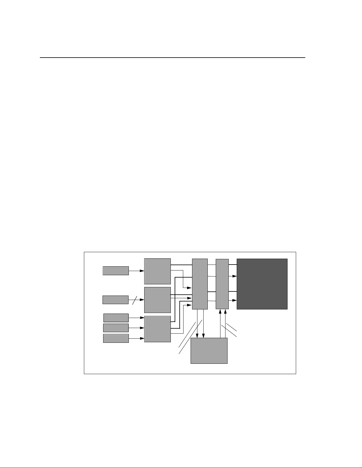
multiplexers are configured for daughter card use. The figure below illustrates the input
port configurations. The on board CBT multiplexer input modes are controlled via the
CPLD control register 1 as discussed in section 2.12.
Figure 2-1, TMS320DM6467 Video Input Port Interfaces
Y
Pr
Composite
In
S-Video In
Component
Video In
THP5147
TMS320C6467
VP_DOUT0-7
VP_CLKO2
VP_DOUT8-15
VP_CLKO3
DC_P2
CBT
MUX
DISABLE ON BOARD VIDEO PORT HI
DISABLE ON BOARD VIDEO PORT LOW
VIDEO_OUT_EN0
CPLD
Video
Decoder
Y0
Y7
THP5147
Video
Decoder
Y0
Y7
TVP7002
Video
Decoder
Y0
Y7
C7
C0
Pb
2
Composite
Video In
S-Video
In
VIDEO_OUT_EN1
Spectrum Digital, Inc
2-5
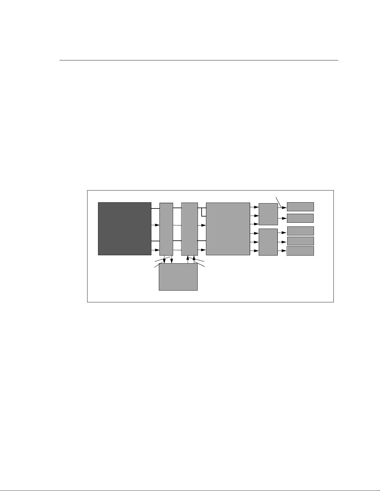
2.5.2 Video Output Port Interfaces
The TMS320DM6467 EVM has a 16 bit wide video output port which directly interface
to an ADV7343 encoder. The video output ports are actually two 8 bit ports which are
combined into a single 16 bit port for high definition video applications.
The on board encoder can generate composite video, S-video, or component video.
The TMS320DM6467’s output port is directly interfaced to the video encoder via CBT
multiplexers and switches. The on board encoder video inputs can be directly
connected via the daughter card interface in two 8 bit sections when the daughter
card asserts VIDEO_OUT_EN0 and/or VIDEO_OUT_EN1 high.
For the high definition modes Y0-Y7 and C0-C7 inputs are used on the encoder. To
change the on board CBT multiplexer to this mode the CPLD control register 1, bit 6
needs to be programmed to the appropriate mode. The diagram below
illustrates the video port output configuration on the EVM.
Figure 2-2, TMS320DM6467 Video Output Port Interfaces
TMS320C6467 DC_P2 CBT
MUX
and
Switches
S-Video Out
Pr
Pb
Y
Composite
Out
HD/SD
Video
Encoder
DAC6
DAC5
DAC4
DAC3
DAC2
DAC1
THS7314
Video
Amp
THS7034
Video
Amp
THS7034
Video
Amp
HS/HD
Video
Encoder
S0-S7
Inputs
Y0-Y7
Inputs
CLKINA
C0-C7
Inputs
CLKINB
VP_DOUT0-7
VP_CLKO2
VP_DOUT8-15
VP_CLKO3
Composite
S-Video
Out Component
Video Out
CPLD
2
VIDEO_OUT_EN0
VIDEO_OUT_EN1 DISABLE ON BOARD VIDEO PORT LOW
DISABLE ON BOARD VIDEO PORT HI
Spectrum Digital, Inc
2-6 TMS320DM6467 EVM Technical Reference
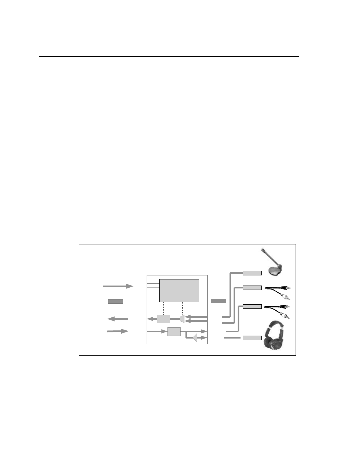
2.6 AIC32 Interface
The EVM uses a Texas Instruments TLV320AIC32 stereo codec for input and output of
audio signals. The codec samples analog signals on the microphone or line inputs and
converts them into digital data so it can be processed by the DSP. When the DSP is
finished with the data it uses the codec to convert the samples back into analog signals
on the line output so the user can hear the output.
The codec communicates using two serial channels, one to control the codec’s internal
configuration registers and one to send and receive digital audio samples. The I2C bus
is used as the unidirectional control channel. The control channel is generally only used
when configuring the codec, it is typically idle when audio data is being transmitted,
The bi-directional data channel interfaces to the on chip McASP0. All audio data flows
through the data channel. Many data formats are supported based on the three
variables of sample width, clock signal source and serial data format. The EVM
examples generally use a 16-bit sample width with the codec in master mode so it
generates the frame sync and bit clocks at the correct sample rate for the McASP.
The codec has a programmable clock from a CDCE949 PLL device which is
configurable via I2C. The default system clock is generated by the CDCE949. The
internal sample rate generate subdivides the default clock to generate common
frequencies. The sample rate generator in the AIC32 is set by I2C command codec
registers. The figure below shows the codec interface on the TMS320DM6467 EVM.
DOUT
DIN
BCLK
WCLK
MIC IN
LINE IN
LINE OUT
HP OUT
M
cASP
I2S Format
AIC32 Codec
Digital Analog
MIC IN
LINE IN
LINE OUT
HP OUT
SCL
SDA
I
2
C
Control
SCL
SDA I
2
C Format
Control Registers
ADC
DAC
AXR[0]
AXR[1]
ACLKR
ACLKX
AFSR
AFSX
Figure 2-3, TMS320DM6467 EVM CODEC INTERFACE
Table of contents
Other Spectrum Digital Motherboard manuals

Spectrum Digital
Spectrum Digital TMS320VC5509A EVM PLUS Use and care manual

Spectrum Digital
Spectrum Digital TMS320C5517 Use and care manual

Spectrum Digital
Spectrum Digital eZdsp F2804 Series Use and care manual

Spectrum Digital
Spectrum Digital eZdsp R2812 USB Use and care manual

Spectrum Digital
Spectrum Digital TMS320DM6437 Use and care manual

Spectrum Digital
Spectrum Digital eZdsp F28 Series Instruction Manual

Spectrum Digital
Spectrum Digital eZdsp F28335 Instruction Manual

Spectrum Digital
Spectrum Digital XDS560v2 Use and care manual

Spectrum Digital
Spectrum Digital TMS320VC5505 Use and care manual

Spectrum Digital
Spectrum Digital TMS320F240 Use and care manual


