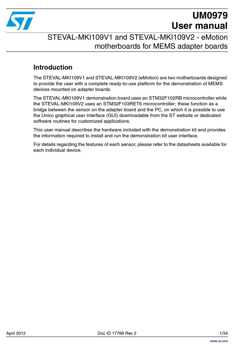
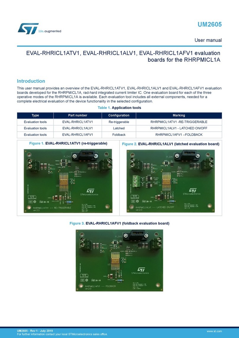
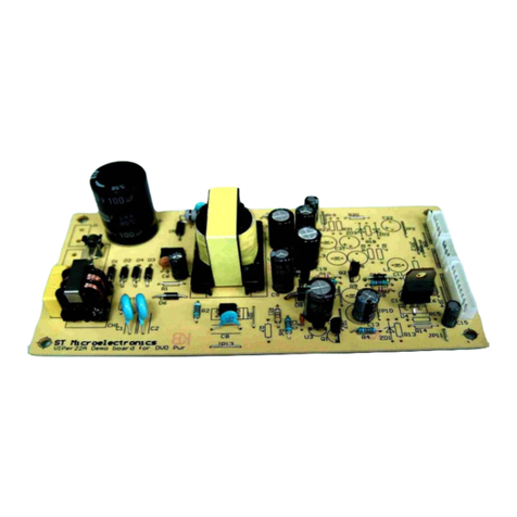
ST ARMIC30 User manual

April 2006 Rev 2 1/35
UM0193
User manual
Getting Started with the ARMIC30 Evaluation Board
(ARM Core-based Industrial Controller using STR730 MCU)
Introduction
This user manual describes the implementation of the ARMIC30 Evaluation Board. The
ARMIC30 can be used to evaluate a variety of devices, especially microcontrollers, with the
added advantage that all pins are available on logically structured and well-documented
header pins.
Applications are based on 32-bit STR730F microcontroller that uses a powerful ARM7TDMI
core providing an extensive range of peripheral functions and enhanced I/O capabilities.
The ARMIC30 is equipped with RS-232, RS-485, CAN, SPI, I²C and JTAG communication
interfaces.
The evaluation board also includes digital input/output connectors and three motor control
connectors with a pinout compatible with PowerSpin evaluation boards (supporting L6205,
-6, -7, -8, and L6235 integrated motor drivers). The output interface is compatible with
VN808 and VN340 Reference Design Boards and the input interface can be used for CLT3-
4BT6 or PCLT-2A evaluation board connections.
Applications can be supplied from a standard DC power supply (7 to 30V DC) or directly
using a 24V DC industrial mains supply.
Complete solution is implemented on double-face board with only two copper layers for
increased cost-effectiveness. Routing accuracy is also cost-optimized.
The ARMIC30 evaluation board package includes a CD-ROM containing the standard
STR730 software library, source code examples, board fabrication data (Gerber files), this
user manual and other related documentation.
Key Features
■32-bit STR730FZ2T7 microcontroller with 36-MHz ARM7TDMI CPU core
■RS-232 interface with 15kV guaranteed ESD protection using ST202E transceiver
■RS-485 interface using ST485A high-speed transceiver with bit rates up to 30 Mbps
■L9616 high-speed CAN driver with communication speeds up to 1 Mbps
■SPI and I²C communication connectors
■8-bit digital input/output connectors
■3 Motor Control connectors
■STM811 small reset circuit
■Power supply using L5973AD DC/DC converter
■6 to 30V DC supply voltage range
www.st.com
Contents UM0193
2/35
Contents
1 Hardware . . . . . . . . . . . . . . . . . . . . . . . . . . . . . . . . . . . . . . . . . . . . . . . . . . 3
1.1 RS-232 interface . . . . . . . . . . . . . . . . . . . . . . . . . . . . . . . . . . . . . . . . . . . . 4
1.2 RS-485 interface . . . . . . . . . . . . . . . . . . . . . . . . . . . . . . . . . . . . . . . . . . . . 5
1.3 CAN interface . . . . . . . . . . . . . . . . . . . . . . . . . . . . . . . . . . . . . . . . . . . . . . . 6
1.4 SPI interface . . . . . . . . . . . . . . . . . . . . . . . . . . . . . . . . . . . . . . . . . . . . . . . . 7
1.5 I²C interface . . . . . . . . . . . . . . . . . . . . . . . . . . . . . . . . . . . . . . . . . . . . . . . . 8
1.6 JTAG interface . . . . . . . . . . . . . . . . . . . . . . . . . . . . . . . . . . . . . . . . . . . . . . 8
1.6.1 JTAG supply voltages . . . . . . . . . . . . . . . . . . . . . . . . . . . . . . . . . . . . . . . 9
1.7 General purpose connectors . . . . . . . . . . . . . . . . . . . . . . . . . . . . . . . . . . 10
1.7.1 General purpose input connector . . . . . . . . . . . . . . . . . . . . . . . . . . . . . 10
1.7.2 General purpose output connector . . . . . . . . . . . . . . . . . . . . . . . . . . . . 11
1.7.3 General purpose motor control connectors . . . . . . . . . . . . . . . . . . . . . . 12
1.8 LED indicators . . . . . . . . . . . . . . . . . . . . . . . . . . . . . . . . . . . . . . . . . . . . . 13
1.9 Power supplies . . . . . . . . . . . . . . . . . . . . . . . . . . . . . . . . . . . . . . . . . . . . . 14
1.10 Timing . . . . . . . . . . . . . . . . . . . . . . . . . . . . . . . . . . . . . . . . . . . . . . . . . . . . 15
1.11 Reset . . . . . . . . . . . . . . . . . . . . . . . . . . . . . . . . . . . . . . . . . . . . . . . . . . . . 15
1.12 Boot mode selection . . . . . . . . . . . . . . . . . . . . . . . . . . . . . . . . . . . . . . . . . 16
2 Software . . . . . . . . . . . . . . . . . . . . . . . . . . . . . . . . . . . . . . . . . . . . . . . . . . 17
3 Electrical specifications and timings . . . . . . . . . . . . . . . . . . . . . . . . . . 18
4 Ordering information . . . . . . . . . . . . . . . . . . . . . . . . . . . . . . . . . . . . . . . 19
Appendix A ARMIC30 board layout. . . . . . . . . . . . . . . . . . . . . . . . . . . . . . . . . . . . 20
Appendix B ARMIC30 schematic diagrams . . . . . . . . . . . . . . . . . . . . . . . . . . . . . 24
Appendix C Jumper settings. . . . . . . . . . . . . . . . . . . . . . . . . . . . . . . . . . . . . . . . . 29
Appendix D Bill of materials . . . . . . . . . . . . . . . . . . . . . . . . . . . . . . . . . . . . . . . . . 31
Revision history . . . . . . . . . . . . . . . . . . . . . . . . . . . . . . . . . . . . . . . . . . . . . . . . . . . . 34

UM0193 Hardware
3/35
1 Hardware
The ARMIC30 Evaluation Board is designed to evaluate and develop Industrial Controller
(IC) applications that use several different communication interfaces as shown in Figure 1.
Figure 1. ARMIC30 Communication interfaces
The ARMIC30 comes on a double-face printed circuit board with only two copper layers.
Circuit routing is Class 5 accuracy meaning that the smallest route/isolation distance is 8 mil
(0.2032 mm) and the smallest hole diameter is 20 mil (0.5080 mm). Board dimensions are
132 x 116 mm.
Figure 2. ARMIC30 board presentation
Ai11696
STR730F
MCU
RS-232
ST202E
RS-485
ST485A
CAN
L9616
SPI
I²C
JTAG
UART0
UART1
CAN0 JTAG
I2C0
BSPI0
8-MHz
Crystal
MCU Reset
RS-485
Connection
CAN
Connection
I²C
Connection
Standard
Power Supply
Connection
Power Supply
Industrial Bus
RS-232
Connection
SPI
Connection Input GP
Connection Output GP
Connection
GP PowerSpin
Connections JTAG
Connection
STR730
MCU
User
LEDs

Hardware UM0193
4/35
1.1 RS-232 interface
The ST202E Transceiver ensures RS-232 communication through the UART0 serial
channel of the STR730F microcontroller as shown in Figure 4.
The maximum speed of this interface is 230 Kbps.
The UART0 channel can be used for simple communication and internal Flash memory
programming (for example, when using the RFLASHER application from Raisonance).
A male, 9-pin D-Sub connector (J8) provides the RS-232 connection. For correct
interconnection with a PC, a “null-modem” cable (crossed Rx | Tx signals) should be used.
Jumper 35 can be used to select Loop mode (for testing purposes) as described in
Appendix C: Jumper settings.
Figure 3. RS-232 (J8), RS-485 (J12) and CAN (J15) connector pinout
Figure 4. RS-232 schematic diagram
Table 1. RS-232 Connections
J8 Pin Signal STR730F MCU Peripheral
2 RxD (Receive Data) Port 6.8 UART0
3 TxD (Transmit Data) Port 6.9 UART0
5GND
1, 4, 6 to 9 Not connected
Shielding Connected to GND by R24 || C23 (100 kΩ|| 4.7 nF)
1 234 5
6789
1 234 5
6789
RS-485 RS-232 and CAN
ETXD0
ERXD0
5V
5V
5V
TxD 232
RxD 232
1 2
J35
R22
10k
R22
10k
1
2
3
4
5
6
7
8
9
M1
M2
J8
R24 M1
C21
100n
C21
100n
R23 0R
C24
100n
n
C20
100n
C1+
1
C1-
3
C2+
4
C2-
5
V+ 2
V- 6
R1OUT
12
R2OUT
9
T1IN
11
T2IN
10
R1IN 13
R2IN 8
T1OUT 14
T2OUT 7
U3
ST202E
U3
ST202E
C23
4n7/500V
22
00n
C22
100n
C19
100n
C19
100n
DSUB9-Plug
Ai11693

UM0193 Hardware
5/35
1.2 RS-485 interface
The ST485A Transceiver ensures RS-485 communication through the UART1 serial
channel of the STR730F microcontroller as shown in Figure 5.
The maximum speed of this interface is greater than 30 Mbps.
A female, 9-pin D-Sub connector (J12) provides the RS-485 connection using a standard
Profibus pinout.
The RS-485 channel can be terminated using jumpers J10 and J13 as described in
Appendix C: Jumper settings. Terminating resistors R25, R26 and R28 are selected for a
Type-A Profibus DP cable as shown in Figure 5. These resistors can be replaced with
different values depending on the physical layer implemented.
Figure 5. RS-485 schematic diagram
Table 2. RS-485 Connections
J12 Pin Signal STR730F MCU Peripheral
RxD (Receive Data) Port 2.9 UART1
TxD (Transmit Data) Port 2.8 UART1
DE (Driver Enable) Port 2.10 UART1
5GND
1, 2, 4, 7 and 9 Not connected
Shielding Connected to GND by R31 || C26 (100 kΩ|| 4.7 nF)
Ai11694
5V
5V
5V
5V
TxD485
RxD 485
nDE485
R26 220R
NA
R2 220R
NA
R30 0RR30 0R
1 2
J10J10
R28
390R
NA
R28
390R
NA
1 2
J13J13
R29 0RR29 0R
1
J11J11
R27
390R
R27
390R
1
2
3
4
5
6
7
8
9
M1
M2
J12
J12
RO
1DI
4
GND 5
VCC 8
RE
2DE
3A6
B7
U4
ST485A
4
ST485A
R31 M1R31 M1
C25
100n
C25
100n
R25
390R
NA
R25
390R
NA
C26
4n7/500V
C26
4n7/500V
DSUB9 - Socket

Hardware UM0193
6/35
1.3 CAN interface
The L9616 High-Speed Transceiver provides the Controller Area Network (CAN)
communication interface through the CAN0 channel of the STR730F microcontroller.
This serial communication can reach speeds up to 1Mbps.
A male, 9-pin D-Sub connector (J15) provides the CAN connection. The CAN channel can
be terminated with a 120Ω resistor using jumper J14 as described in Appendix C: Jumper
settings. The L9616 CAN transceiver has an Adjustable Slope Control (ASC) feature that
sets the slope speed using its ASC pin. This pin can be either hard-connected high or low
using zero-ohm resistors or it can be controlled by MCU Port 2.0 as shown in Figure 6.
Table 4 describes the resistor assembly and control pin signal levels for CAN
communications.
Figure 6. CAN schematic diagram
Table 3. CAN Connections
J15 Pin Signal STR730F MCU Peripheral
RxD (Receive Data) Port 1.14 CAN0
TxD (Transmit Data) Port 1.15 CAN0
ASC (Adjustable Slope Control) Port 2.0 CAN0
2 CAN Low differential data
7 CAN High differential data
3 Shorted to 6. Connected to GND by R35 / 0Ω
6 Shorted to 3. Connected to GND by R35 / 0Ω
1, 4, 5, 8 and 9 Not connected
Shielding Connected to GND by R36 || C28 (100 kΩ|| 4.7 nF)
Ai11695
5V
5V
5V
C28C28
1
2
3
4
5
6
7
8
U5
RR36 M1
RR35 0R
1
2
3
4
5
6
7
8
9
M1
M2
1 2
DSUB9 - Plug
4n7/500V
C27
100 nF
RX1_Ref
CAN_L
CAN_H
VS
TX0
RX0
ASC
GND
L9616
R34
0R
NA
R33 120R J14 J15
R32
0R
NA
TxD CAN
RxD CAN
ASC CAN

UM0193 Hardware
7/35
Note: 1 If using a resistor assembly (hardware option), the correct MCU signal must be set as an
input!
2 Do not assemble both resistors as this will short-circuit the supply voltage!
1.4 SPI interface
A 10-pin connector (J18) provides the Serial Peripheral Interface (SPI) through the BSPI0
channel of the STR730F microcontroller as shown in Figure 7.
Connector J18 also provides additional general purpose signals that are primarily used as
Watchdog (WD) and Slave Chip Select (SSn) lines.
Figure 7. SPI connector pinout
Table 4. CAN slew rate settings
Speed Slew Rate (V/µs) MCU SIgnal Signal Level Resistor
Low 5 to 20 P2.0 High R32
High 20 to 50 Low R34
Table 5. SPI Connections
J18 Pin Signal STR730F MCU Peripheral
1GND
2+5VDC
3 MOSI (Master Output/Slave Input) Port 6.12 BSPI0
4 MISO (Master Input/Slave Output) Port 6.11 BSPI0
5 SCK (Serial Clock) Port 6.13 BSPI0
6 WD Port 0.12 GPIO
7 SS0 (Slave Select 0) Port 6.14 BSPI0
8 SS1 (Slave Select 1) Port 0.13 GPIO
9 SS2 (Slave Select 2) Port 1.12 GPIO
10 SS3 (Slave Select 3) Port 1.13 GPIO
1
2
3
4
5
6
7
8
9
10

Hardware UM0193
8/35
1.5 I²C interface
A 10-pin connector (J28) provides the Inter-Integrated Circuit (I²C) through the I2C0 channel
of the STR730F microcontroller as shown in Figure 8.
Connector J28 also provides additional general purpose signals (GP0, GP1 and GP2).
Figure 8. I²C connector pinout
1.6 JTAG interface
A 20-pin connector (J7) provides the JTAG interface as shown in Figure 9.
This interface is primarily used for communicating with a PC using suitable converter box
such as J-Link from IAR Systems or R-Link from Raisonance, etc. There exists a wide
choice of development tools on the market supporting microcontroller Flash memory
programming and application debugging.
Figure 9. JTAG connector pinout
Table 6. I²C Connections
J28 Pin Signal STR730F MCU Peripheral
1GND
2+5VDC
3 SDA (Serial Data) Port 2.15 I2C0
4 Not connected
5 SCL (Serial Clock) Port 2.14 I2C0
6 Not connected
7 GP0 Port 3.2 GPIO
8 GP1 Port 3.1 GPIO
9 GP2 Port 3.0 GPIO
10 Not connected
1
2
3
4
5
6
7
8
9
10
1
2
3
4
5
6
7
8
9
10 12 14
11 13 15
16 18 20
17 19

UM0193 Hardware
9/35
Figure 10. JTAG schematic diagram
1.6.1 JTAG supply voltages
A +3.3V DC supply voltage placed on pins 1 and 2 is provided by the DC/DC converter (U6)
reference pin or a separate linear voltage regulator (U7). Please verify the consumption of
any device (for example, converter box) connected to this connector. According to the
device datasheet, the reference pin can deliver a maximum current of 5mA, providing an
accurate voltage level. If the consumption is higher, select the linear voltage regulator (U7)
for the supply connector using jumper J33 as described in Appendix C: Jumper settings.
Certain converter boxes provide a +5V DC supply voltage for the JTAG interface. The new
generation J-link from IAR Systems (the yellow one) provides the supply voltage on pin
number 19. For applications using supplies from the converter box, connect a wire from pin
number 19 of the JTAG (J7) connector to closest +5V DC supply point (for example, J19
right pin). For JTAG communication functions, jumper J32 must be connected and jumper
J33 set to the "lin" position when a +5V DC voltage supply is used.
Caution: Using a supply from a converter box is not recommended for application development or
testing. Accidental short-circuits may damage USB host or converter box circuits.
Table 7. JTAG connections
Pin Signal Pin Signal
1 +3.3V DC 2 +3.3V DC
3JTRST 4GND
5JTDI 6GND
7JTMS 8GND
9JTCK 10GND
11 Connected to GND by R18 (10kΩ)12GND
13 JTDO 14 GND
15 RESET 16 GND
17 Connected to GND by R20 (10kΩ)18GND
19 Connected to GND by R21 (10kΩ)20GND
Ai11699
1 2
3 4
5 6
7 8
910
11 12
13 14
15 16
17 18
19 20
3V3 3V3 3V3 3V3 3V3 3V3
3V3
3V3
C51
100 nF
3V3
C18
100 nF
3V3
C52
10M/16V
+
CON20A
3V3 J7
R18
10k R19
10k R20
10k R21
10k
D2
BZX84C3V3/SOT
R17 430R
nJTRST
JTDI
JTMS
JTCK
JTDO
nRST_EXT
R11
10k
NA
R12
10k R13
10k R14
10k R15
10k
NA
R16
10k
NA

Hardware UM0193
10/35
1.7 General purpose connectors
The ARMIC30 Evaluation Board provides two 8-bit general purpose I/O connectors (J17
and J27) and three general purpose motor control connectors (J20, J22 and J24) that can
be used with current or future extension modules included in STMicroelectronics’ offer
(VN340 / VN808 / VN808CM Reference design boards, CLT3-4BT6 / PCLT-2A test boards,
PowerSpin family of motor control drivers evaluation boards, etc.) or other applications
developed by customers.
1.7.1 General purpose input connector
Jumpers J16 and J25 configure the supply voltage for the 8-bit input connector as described
in Appendix C: Jumper settings. The GP input connector is compatible with Current Limited
Termination (CLT) and Programmable Current Limited Termination (PCLT) applications.
Figure 11. GPIO input connector pinout
Table 8. 8-bit Input GPIO Connections
J17 Pin Signal STR730F MCU Peripheral
1 +5V DC connected by jumper J16
2 GND connected by jumper J25
3 D7 Port 0.7 GPIO
4 D6 Port 0.6 GPIO
5 D5 Port 0.5 GPIO
6 D4 Port 0.4 GPIO
7 D3 Port 0.3 GPIO
8 D2 Port 0.2 GPIO
9 D1 Port 0.1 GPIO
10 D0 Port 0.0 GPIO
1
2
3
4
5
6
7
8
9
10

UM0193 Hardware
11/35
1.7.2 General purpose output connector
Jumpers J26 and J29 configure the supply voltage for the 8-bit output connector as
described in Appendix C: Jumper settings. The GP output connector is compatible with
VN808 and VN340 Evaluation Boards.
Figure 12. GPIO output connector pinout
Table 9. J27 8-bit Output GPIO connections
J27 Pin Signal STR730F MCU Peripheral
1 +5V DC connected by jumper J26
2 GND connected by jumper J29
3 STATUS0 Port 1.11 GPIO
4 D7 Port 1.7 GPIO
5 D6 Port 1.6 GPIO
6 D5 Port 1.5 GPIO
7 D4 Port 1.4 GPIO
8 D3 Port 1.3 GPIO
9 D2 Port 1.2 GPIO
10 D1 Port 1.1 GPIO
11 D0 Port 1.0 GPIO
12 STATUS3 Port 1.8 GPIO
13 STATUS2 Port 1.9 GPIO
14 STATUS1 Port 1.10 GPIO
1
2
3
4
5
6
7
8
9
10 12 14
11 13

Hardware UM0193
12/35
1.7.3 General purpose motor control connectors
Jumpers J19, J21 and J23 configure the supply voltages for the J20, J22 and J24 motor
control connectors, respectively, as described in Appendix C: Jumper settings.
The GP Motor control connectors are compatible with the PowerSpin set of evaluation
boards that are based on monolithic motor control chips. The PowerSpin chip family
includes L6205 -6 -7 -8 and L6235 devices.
Figure 13. GPIO motor control connector pinout
Table 10. 8-bit GPIO/Motor Control Connections
Pin No. J20 MCU Connection J22 MCU Connection J24 MCU Connection Periph.
1+5V DC supply
connected by Jumper
J19
+5V DC supply
connected by Jumper
J21
+5V DC supply
connected by Jumper
J23
2 P3.12 / INT2 P5.12 / INT10 P5.11 / INT9 INT
3 P3.10 P3.8 P3.6 AIN
4 P3.13 / INT3 P5.13 / INT11 P5.10 / INT8 INT
7 P3.11 P3.9 P3.7 AIN
8 P3.15 / INT5 P5.15 / INT13 P5.8 / INT6 INT
10 P4.0 P6.0 P5.7 GPIO
14 P4.1 P6.1 P5.6 GPIO
20 P4.2 P6.2 P5.5 GPIO
22 P0.9 P0.14 P0.11 OCMP
23 GND GND GND
26 P3.14 P5.14 P5.9 INT
28 P0.8 P0.15 P0.10 OCMP
31 PWM5 || cathode of
diode D3 connected to
GND
PWM1 || cathode of
diode D4 connected to
GND
PWM3 || cathode of
diode D5 connected to
GND PWM
32 P1.8 P2.12 P2.13 INT
33 PWM4 || cathode of
diode D3 connected to
GND
PWM0 || cathode of
diode D4 connected to
GND
PWM2 || cathode of
diode D5 connected to
GND PWM
5, 6, 9, 11-
13, 15-19,
21, 24, 25,
27, 29, 30
and 34
Not connected Not connected Not connected
1
2
3
4
5
6
7
8
9
10 12 14
11 13 15 17 19 21 23 25 27 29 31 33
16 18 20 22 24 26 28 30 32 34

UM0193 Hardware
13/35
1.8 LED indicators
The ARMIC30 Evaluation Board includes an LED (D13) indicating a the presence of the +5V
DC supply voltage and four additional LEDs (D9, D10, D11 and D12). These four LEDs can
be individually configured through the STR730F MCU as described in Table 11.
Figure 14. LED schematic diagram
Table 11. LED Connections
LED STR730F MCU Peripheral
D9 Port 4.9 GPIO
D10 Port 4.10 GPIO
D11 Port 4.11 GPIO
D12 Port 4.12 GPIO
+5V DC
Rx
1.5 kΩ
Dx
Green LED
Port 4.x

Hardware UM0193
14/35
1.9 Power supplies
The L5973AD DC/DC converter (U6) supplies the ARMIC30 Evaluation Board with a +5V
DC voltage supply using feedback resistors (R37 and R38) as shown in Figure 15. A green
LED (D13) lights up when this supply is present.
An additional +3.3V DC linear voltage regulator (U7) connected in cascade to the DC/DC
converter output can be used to supply the JTAG connector and level converting resistors
with a +3.3V DC supply voltage. Use jumper J33 to select either a DC/DC reference voltage
or a linear regulator as described in Section 1.6.1: JTAG supply voltages and Appendix C:
Jumper settings.
Connectors J30 or J31 provide the ARMIC30 Evaluation Board power supplies. Connector
J30 includes a polarity protection diode and is suitable for use with a standard mains
adapter having an output voltage range between +7 and +30V DC. Connector J31 is
connected directly to the DC/DC converter input which is over-voltage protected by a transil
diode (D8) for a recommended supply voltage range between +6 and +30V DC. The
ARMIC30 Evaluation Board clearly indicates the power supply polarity.
Figure 15. Power supply schematic diagram
5V_TP
5V
3V3
5V 5V 5V 5V
1 2
J34J34
STPS340U
D7
STPS340U
D7
+
COMP
4
INH
3
Vin
8
SYNC
2FB 5
OUT 1
VREF
6
GND
7GND
9
U6U6 1 2
J32J32
+
R38
3k9
R38
3k9
C38
100n
C38
100n
++
R39
6k2
R39
6k2
C36
22nF
C36
22nF
C37
100n
C37
100n
+
1
2
3
J33J33
R37
12k
R37
12k
L1L1
1
2
1
2
3
C35
100pF
C35
100pF
+
GND
4
VOUT 3
VIN
1
Ai12503
C43
10M/16V
C42
10M/16V
C41
10M/16V
C40
10M/16V
LF33/DPAK
U7
C34
100 µF
16V
5V_TP
33 µH
C33
10 µF
35V
D8
SM6T33A
D6
STPS340U
J30
PS CON
J31
24V Terminal Block
L5973AD
C39
2M2/16V

UM0193 Hardware
15/35
1.10 Timing
The ARMIC30 Evaluation Board uses a simple 8-MHz crystal assembly for timing as shown
in Figure 16.
Figure 16. Crystal assembly
1.11 Reset
The ARMIC30 Evaluation Board includes a reset circuit used to reset the STR730 MCU
using an STM811 Reset Circuit (U2) as shown in Figure 17.
Figure 17. Reset circuit assembly
XTAL1
XTAL2
C15
15p
C15
15p
C14
15p
C14
15p
Y1Y1
R5
1k
R5
1k
Ai12500
8 MHz
R6
1M5
Ai12501
5V
5V
SW1
R7
4k7
R7
4k7
GND
1
RST
2
MR
3
VCC 4
U2
D1
BAT54A/SOT
nRST_EXT
nRST
STM811

Hardware UM0193
16/35
1.12 Boot mode selection
The ARMIC30 Evaluation Board includes a Boot mode selection circuit as shown in
Figure 18.
This feature selects boot memory access using Jumpers J5 and J6 as described in
Appendix C: Jumper settings.
For more information, please refer to the STR730 Reference Manual.
Figure 18. Boot mode selection circuit assembly
nRST
5V
5V
M1
M0
1
2
3
J6J6
C17
1n
C17
1n
1
2
3
J5J5
C16
100n
C16
100n
R8
1k
R8
1k
R10
47k
R10
47k
R9
3k3
R9
3k3
Ai12502
T1
BC847C

UM0193 Software
17/35
2 Software
The CD-ROM delivered with the ARMIC30 Evaluation Board contains several software
examples demonstrating the use of microcontroller peripheral circuits. These examples use
the standard STR730 software library which is available on www.st.com. Examples are
created using the IAR Embedded Workbench for ARM development tools and appropriate
project files are available on the CD-ROM.
The STR730 microcontroller is delivered pre-programmed with the “GPIO_ARMIC”
example.

Electrical specifications and timings UM0193
18/35
3 Electrical specifications and timings
Table 12. ARMIC30 evaluation board technical data
Parameter Conditions Min. Typ. Max. Unit
Recommended board supply voltage range From connector J30
From connector J31 7
630
30 V DC
Complete application power consumption (1)(2) Run mode w/out Load,
VS= 24V DC applied to J31,
fCPU = 36 MHz
26
624 mA
mW
1. This value is not accurate and is for information only. MCU peripherals are not initialized and their pins supplied with static
values. Program is running from internal Flash memory, working in an endless loop, performing only a branch instruction.
All microcontroller peripherals are disabled, CMU is on and PLL is on.
2. Power consumption is measured with a 24V DC supply from J31 connector.
Table 13. ARMIC30 GPIO technical data
Parameter Conditions Min. Typ. Max. Unit
Input Low Level -0.3 0.8 V DC
Input High Level 2 5.3
Output Low Level Push Pull, IOL = 2mA 0 0.4 V DC
Output High Level Push Pull, IOH = 2mA 4.2 5
Table 14. ARMIC30 bus interface data
Parameter Conditions Min. Typ. Max. Unit
RS-232 channel speed 230 Kbps
RS-485 channel speed 30 Mbps
CAN channel speed 1Mbps

ARMIC30 board layout UM0193
20/35
Appendix A ARMIC30 board layout
This section describes the layout of ARMIC30 Evaluation Board PCB.
Figure 19. ARMIC30 top layer
Table of contents
Other ST Motherboard manuals

ST
ST STEVAL-ISB042V1 User manual

ST
ST SPC58XXMB User manual

ST
ST STM32L476ZG User manual

ST
ST STM32L152-EVAL Installation and operating instructions

ST
ST STEVAL-ISF003V1 User manual

ST
ST UM0527 User manual

ST
ST eMotion STEVAL-MKI109V1 User manual

ST
ST STM32F4 Series Installation and operating instructions

ST
ST SPC572L-DISP User manual

ST
ST STM32303C-EVAL User manual
Popular Motherboard manuals by other brands

Digilent
Digilent Orbit BoosterPack Basic Demo user guide

ASROCK
ASROCK H81M-VG4 R2.0 user manual

ASROCK
ASROCK QC5000-ITX/WiFi manual

Infineon Technologies
Infineon Technologies Cypress MB39C503-EVBSK-01 Operation manual

Analog Devices
Analog Devices ADSP-BF526 EZ-Board manual

Supermicro
Supermicro X6DAi-G user manual