ST UM1935 User manual

September 2015 DocID028194 Rev 1 1/77
1
UM1935
User manual
Evaluation board with STM32F479NI MCU
Introduction
The STM32479I-EVAL evaluation board is a complete demonstration and development
platform for STMicroelectronics ARM®Cortex® -M4 core-based STM32F479NIH6
microcontroller. It features three I2C, six SPIs with two multiplexed full-duplex I2S interfaces,
SDMMC, four USARTs and four UARTs, two CANs, three 12-bit ADCs, two 12-bit DACs,
one SAI, 8 to 14-bit digital camera module interface, internal 320+4 Kbytes of SRAM and 2
Mbytes of Flash memory, USB HS OTG and USB FS OTG, Ethernet MAC, FMC interface,
MIPI DSI interface, Quad-SPI interface, Cryptographic acceleration, JTAG and ETM
debugging support. This evaluation board can be used as a reference design for user
application development but it cannot be considered as a final application.
The full range of hardware features on the board helps the user to evaluate all peripherals
(USB OTG HS, USB OTG FS, Ethernet, motor control, CAN, microSD Card, USART, Audio
DAC and ADC, digital microphone, IrDA, RF-EEPROM, SRAM, NOR Flash, SDRAM,
Quad-SPI Flash, 4" TFT LCD with MIPI DSI interface and capacitive touch panel and
others) and to develop his own applications. Extension headers make it possible to easily
connect a daughterboard for specific application.
The integrated ST-LINK/V2-1 provides an embedded in-circuit debugger and programmer
for the STM32 MCU.
Figure 1. STM32479I-EVAL evaluation board
1. Picture not contractual.
www.st.com

Contents UM1935
2/77 DocID028194 Rev 1
Contents
1 Features . . . . . . . . . . . . . . . . . . . . . . . . . . . . . . . . . . . . . . . . . . . . . . . . . . . 6
2 Demonstration software . . . . . . . . . . . . . . . . . . . . . . . . . . . . . . . . . . . . . . 7
3 Order code . . . . . . . . . . . . . . . . . . . . . . . . . . . . . . . . . . . . . . . . . . . . . . . . . 7
4 Delivery recommendations . . . . . . . . . . . . . . . . . . . . . . . . . . . . . . . . . . . 7
5 Hardware Layout and configuration . . . . . . . . . . . . . . . . . . . . . . . . . . . . 8
5.1 Embedded ST-LINK/V2-1 . . . . . . . . . . . . . . . . . . . . . . . . . . . . . . . . . . . . . .11
5.1.1 Drivers . . . . . . . . . . . . . . . . . . . . . . . . . . . . . . . . . . . . . . . . . . . . . . . . . . 11
5.1.2 ST-LINK/V2-1 firmware upgrade . . . . . . . . . . . . . . . . . . . . . . . . . . . . . . 12
5.2 Power Supply . . . . . . . . . . . . . . . . . . . . . . . . . . . . . . . . . . . . . . . . . . . . . . 12
5.3 Clock source . . . . . . . . . . . . . . . . . . . . . . . . . . . . . . . . . . . . . . . . . . . . . . . 15
5.4 Reset source . . . . . . . . . . . . . . . . . . . . . . . . . . . . . . . . . . . . . . . . . . . . . . 16
5.5 Boot option . . . . . . . . . . . . . . . . . . . . . . . . . . . . . . . . . . . . . . . . . . . . . . . . 17
5.6 Audio . . . . . . . . . . . . . . . . . . . . . . . . . . . . . . . . . . . . . . . . . . . . . . . . . . . . 17
5.7 USB OTG1 FS . . . . . . . . . . . . . . . . . . . . . . . . . . . . . . . . . . . . . . . . . . . . . 19
5.8 USB OTG2 HS and FS . . . . . . . . . . . . . . . . . . . . . . . . . . . . . . . . . . . . . . . 20
5.9 RS232 and IrDA . . . . . . . . . . . . . . . . . . . . . . . . . . . . . . . . . . . . . . . . . . . . 20
5.10 MicroSD card . . . . . . . . . . . . . . . . . . . . . . . . . . . . . . . . . . . . . . . . . . . . . . 21
5.11 RF-EEPROM . . . . . . . . . . . . . . . . . . . . . . . . . . . . . . . . . . . . . . . . . . . . . . 21
5.12 CAN . . . . . . . . . . . . . . . . . . . . . . . . . . . . . . . . . . . . . . . . . . . . . . . . . . . . . 22
5.13 Ethernet . . . . . . . . . . . . . . . . . . . . . . . . . . . . . . . . . . . . . . . . . . . . . . . . . . 22
5.14 Memories . . . . . . . . . . . . . . . . . . . . . . . . . . . . . . . . . . . . . . . . . . . . . . . . . 23
5.15 Quad-SPI NOR Flash . . . . . . . . . . . . . . . . . . . . . . . . . . . . . . . . . . . . . . . . 24
5.16 Analog input . . . . . . . . . . . . . . . . . . . . . . . . . . . . . . . . . . . . . . . . . . . . . . . 24
5.17 Camera module . . . . . . . . . . . . . . . . . . . . . . . . . . . . . . . . . . . . . . . . . . . . 25
5.18 Display and input devices . . . . . . . . . . . . . . . . . . . . . . . . . . . . . . . . . . . . . 25
5.19 Motor control . . . . . . . . . . . . . . . . . . . . . . . . . . . . . . . . . . . . . . . . . . . . . . 26
5.20 MFX (Multi Function eXpander) . . . . . . . . . . . . . . . . . . . . . . . . . . . . . . . . 28

DocID028194 Rev 1 3/77
UM1935 Contents
3
6 Connectors . . . . . . . . . . . . . . . . . . . . . . . . . . . . . . . . . . . . . . . . . . . . . . . 30
6.1 Motor control connector CN1 . . . . . . . . . . . . . . . . . . . . . . . . . . . . . . . . . . 30
6.2 RF-EEPROM daughterboard connector CN2 . . . . . . . . . . . . . . . . . . . . . 31
6.3 Analog input connector CN3 . . . . . . . . . . . . . . . . . . . . . . . . . . . . . . . . . . 31
6.4 Camera module connector CN4 . . . . . . . . . . . . . . . . . . . . . . . . . . . . . . . . 32
6.5 Daughterboard extension connectors CN5 and CN6 . . . . . . . . . . . . . . . . 33
6.6 RS232 connector CN7 . . . . . . . . . . . . . . . . . . . . . . . . . . . . . . . . . . . . . . . 37
6.7 USB OTG2 HS micro-AB connector CN8 . . . . . . . . . . . . . . . . . . . . . . . . 38
6.8 Ethernet RJ45 connector CN9 . . . . . . . . . . . . . . . . . . . . . . . . . . . . . . . . . 38
6.9 Memory connectors CN10 and CN11 . . . . . . . . . . . . . . . . . . . . . . . . . . . . 39
6.10 ETM trace debugging connector CN12 . . . . . . . . . . . . . . . . . . . . . . . . . . 42
6.11 USB OTG1 FS Micro-AB connector CN13 . . . . . . . . . . . . . . . . . . . . . . . . 42
6.12 USB OTG2 FS Micro-AB connector CN14 . . . . . . . . . . . . . . . . . . . . . . . . 43
6.13 TFT LCD connector CN15 . . . . . . . . . . . . . . . . . . . . . . . . . . . . . . . . . . . . 43
6.14 JTAG/SWD connector CN16 . . . . . . . . . . . . . . . . . . . . . . . . . . . . . . . . . . 44
6.15 MicroSD connector CN17 . . . . . . . . . . . . . . . . . . . . . . . . . . . . . . . . . . . . . 45
6.16 Power connector CN19 . . . . . . . . . . . . . . . . . . . . . . . . . . . . . . . . . . . . . . 45
6.17 ST-LINK/V2-1 programming connector CN20 . . . . . . . . . . . . . . . . . . . . . 46
6.18 MFX programming connector CN21 . . . . . . . . . . . . . . . . . . . . . . . . . . . . . 46
6.19 ST-LINK/V2-1 USB type B connector CN22 . . . . . . . . . . . . . . . . . . . . . . . 46
6.20 CAN D-type 9-pins male connector CN23 . . . . . . . . . . . . . . . . . . . . . . . . 47
6.21 MEMS microphone coupon connectors CN25 and CN28 . . . . . . . . . . . . 47
6.22 Audio jack (Speaker) CN26 . . . . . . . . . . . . . . . . . . . . . . . . . . . . . . . . . . . 48
6.23 Audio jack CN27 . . . . . . . . . . . . . . . . . . . . . . . . . . . . . . . . . . . . . . . . . . . . 48
7 Schematics . . . . . . . . . . . . . . . . . . . . . . . . . . . . . . . . . . . . . . . . . . . . . . . 49
8 Appendix A STM32479I-EVAL I/O assignment . . . . . . . . . . . . . . . . . . . 68
9 Appendix B Mechanical dimensions . . . . . . . . . . . . . . . . . . . . . . . . . . . 75
10 Revision History . . . . . . . . . . . . . . . . . . . . . . . . . . . . . . . . . . . . . . . . . . . 76

List of tables UM1935
4/77 DocID028194 Rev 1
List of tables
Table 1. Power related jumpers . . . . . . . . . . . . . . . . . . . . . . . . . . . . . . . . . . . . . . . . . . . . . . . . . . . . 14
Table 2. 25MHz Crystal X1 related solder bridges . . . . . . . . . . . . . . . . . . . . . . . . . . . . . . . . . . . . . . 16
Table 3. 32KHz Crystal X2 related solder bridges . . . . . . . . . . . . . . . . . . . . . . . . . . . . . . . . . . . . . . 16
Table 4. Boot related switch . . . . . . . . . . . . . . . . . . . . . . . . . . . . . . . . . . . . . . . . . . . . . . . . . . . . . . . 17
Table 5. Boot0 related jumpers. . . . . . . . . . . . . . . . . . . . . . . . . . . . . . . . . . . . . . . . . . . . . . . . . . . . . 17
Table 6. Audio related jumpers. . . . . . . . . . . . . . . . . . . . . . . . . . . . . . . . . . . . . . . . . . . . . . . . . . . . . 18
Table 7. USB OTG2 function configuration . . . . . . . . . . . . . . . . . . . . . . . . . . . . . . . . . . . . . . . . . . . 20
Table 8. USART1 related jumpers . . . . . . . . . . . . . . . . . . . . . . . . . . . . . . . . . . . . . . . . . . . . . . . . . . 21
Table 9. CAN related jumpers . . . . . . . . . . . . . . . . . . . . . . . . . . . . . . . . . . . . . . . . . . . . . . . . . . . . . 22
Table 10. Ethernet related jumpers . . . . . . . . . . . . . . . . . . . . . . . . . . . . . . . . . . . . . . . . . . . . . . . . . . 22
Table 11. Ethernet related solder bridges. . . . . . . . . . . . . . . . . . . . . . . . . . . . . . . . . . . . . . . . . . . . . . 23
Table 12. NOR Flash related jumpers . . . . . . . . . . . . . . . . . . . . . . . . . . . . . . . . . . . . . . . . . . . . . . . . 23
Table 13. Analog input related jumpers . . . . . . . . . . . . . . . . . . . . . . . . . . . . . . . . . . . . . . . . . . . . . . . 24
Table 14. LCD modules connector (CN15). . . . . . . . . . . . . . . . . . . . . . . . . . . . . . . . . . . . . . . . . . . . . 25
Table 15. Motor control related solder bridges . . . . . . . . . . . . . . . . . . . . . . . . . . . . . . . . . . . . . . . . . . 28
Table 16. MFX signals . . . . . . . . . . . . . . . . . . . . . . . . . . . . . . . . . . . . . . . . . . . . . . . . . . . . . . . . . . . . 28
Table 17. Motor control connector CN1 . . . . . . . . . . . . . . . . . . . . . . . . . . . . . . . . . . . . . . . . . . . . . . . 30
Table 18. RF-EEPROM daughterboard connector CN2 . . . . . . . . . . . . . . . . . . . . . . . . . . . . . . . . . . . 31
Table 19. Analog input-output connector CN3 . . . . . . . . . . . . . . . . . . . . . . . . . . . . . . . . . . . . . . . . . . 32
Table 20. Camera module connector CN4 . . . . . . . . . . . . . . . . . . . . . . . . . . . . . . . . . . . . . . . . . . . . . 32
Table 21. Daughterboard extension connector CN5 . . . . . . . . . . . . . . . . . . . . . . . . . . . . . . . . . . . . . 33
Table 22. Daughterboard extension connector CN6 . . . . . . . . . . . . . . . . . . . . . . . . . . . . . . . . . . . . . 35
Table 23. RS232 connector CN7 with ISP support. . . . . . . . . . . . . . . . . . . . . . . . . . . . . . . . . . . . . . . 37
Table 24. USB OTG HS Micro-AB connector CN8 . . . . . . . . . . . . . . . . . . . . . . . . . . . . . . . . . . . . . . . 38
Table 25. RJ45 connector CN9 . . . . . . . . . . . . . . . . . . . . . . . . . . . . . . . . . . . . . . . . . . . . . . . . . . . . . 38
Table 26. Memory connector CN10 . . . . . . . . . . . . . . . . . . . . . . . . . . . . . . . . . . . . . . . . . . . . . . . . . . 39
Table 27. Memory connector CN11 . . . . . . . . . . . . . . . . . . . . . . . . . . . . . . . . . . . . . . . . . . . . . . . . . . 40
Table 28. ETM trace debugging connector CN12 . . . . . . . . . . . . . . . . . . . . . . . . . . . . . . . . . . . . . . . 42
Table 29. USB OTG1 FS Micro-AB connector CN13 . . . . . . . . . . . . . . . . . . . . . . . . . . . . . . . . . . . . . 43
Table 30. USB OTG2 FS Micro-AB connector CN14 . . . . . . . . . . . . . . . . . . . . . . . . . . . . . . . . . . . . 43
Table 31. JTAG/SWD debugging connector CN16 . . . . . . . . . . . . . . . . . . . . . . . . . . . . . . . . . . . . . . 44
Table 32. MicroSD connector CN17 . . . . . . . . . . . . . . . . . . . . . . . . . . . . . . . . . . . . . . . . . . . . . . . . . . 45
Table 33. USB type B connector CN22 . . . . . . . . . . . . . . . . . . . . . . . . . . . . . . . . . . . . . . . . . . . . . . . 46
Table 34. CAN D-type 9-pins male connector CN23 . . . . . . . . . . . . . . . . . . . . . . . . . . . . . . . . . . . . . 47
Table 35. MEMS microphone coupon connectors CN25 and CN28. . . . . . . . . . . . . . . . . . . . . . . . . . 47
Table 36. STM32479I-EVAL I/O assignment . . . . . . . . . . . . . . . . . . . . . . . . . . . . . . . . . . . . . . . . . . . 68
Table 37. Mechanical dimensions . . . . . . . . . . . . . . . . . . . . . . . . . . . . . . . . . . . . . . . . . . . . . . . . . . . 75
Table 38. Document Revision History . . . . . . . . . . . . . . . . . . . . . . . . . . . . . . . . . . . . . . . . . . . . . . . . 76

DocID028194 Rev 1 5/77
UM1935 List of figures
5
List of figures
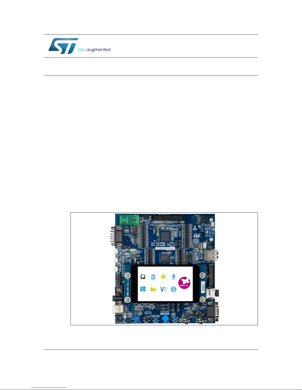
Figure 1. STM32479I-EVAL evaluation board . . . . . . . . . . . . . . . . . . . . . . . . . . . . . . . . . . . . . . . . . . . 1
Figure 2. Hardware Block Diagram . . . . . . . . . . . . . . . . . . . . . . . . . . . . . . . . . . . . . . . . . . . . . . . . . . . 9
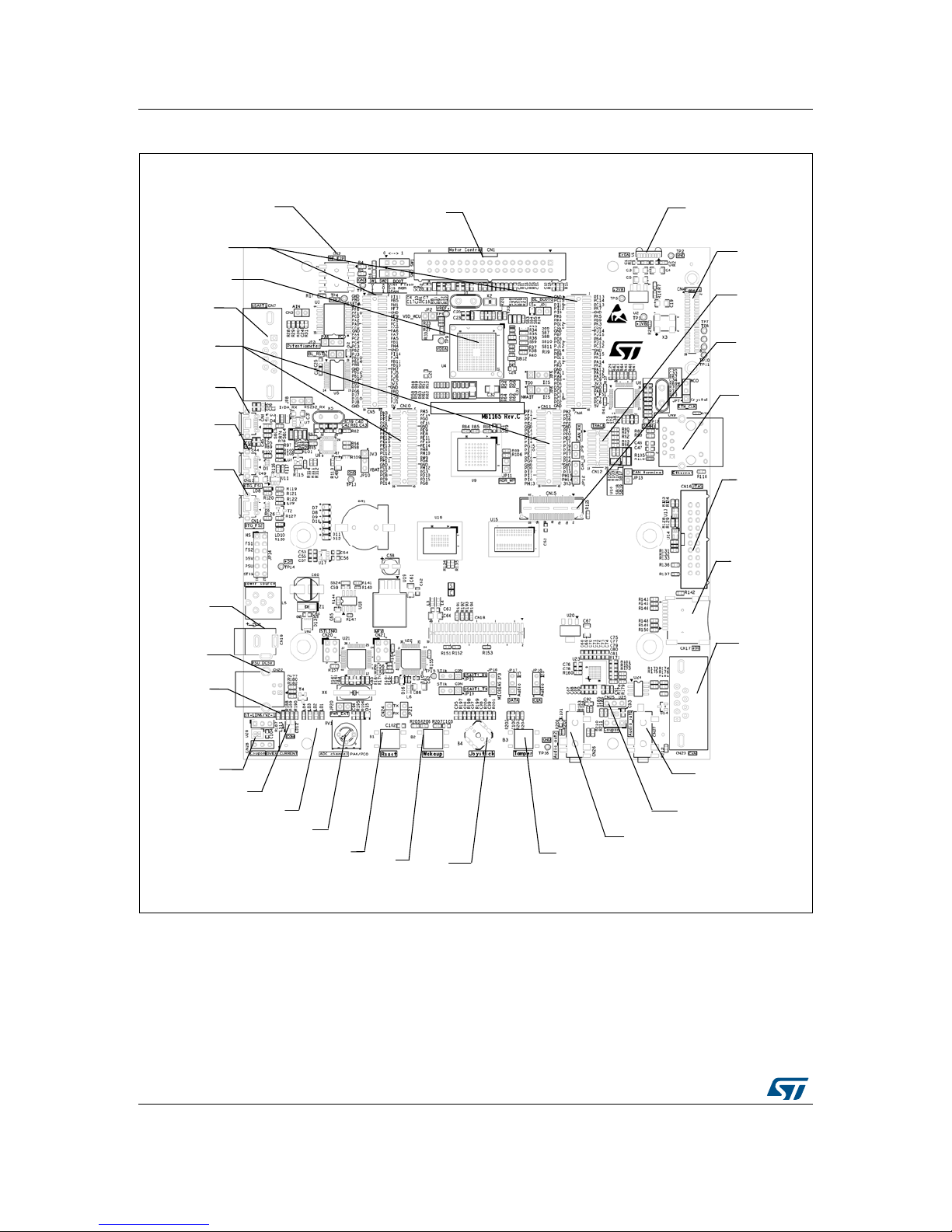
Figure 3. STM32479I-EVAL evaluation board layout. . . . . . . . . . . . . . . . . . . . . . . . . . . . . . . . . . . . . 10
Figure 4. Updating the list of drivers in device manager . . . . . . . . . . . . . . . . . . . . . . . . . . . . . . . . . . 12
Figure 5. STM32479I-EVAL evaluation board motor control PCB reworks (bottom side) . . . . . . . . . 27
Figure 6. STM32479I-EVAL evaluation board motor control PCB reworks (top side) . . . . . . . . . . . . 27
Figure 7. Motor control connector CN1 (top view) . . . . . . . . . . . . . . . . . . . . . . . . . . . . . . . . . . . . . . . 30
Figure 8. RF-EEPROM daughterboard connector CN2 (front view) . . . . . . . . . . . . . . . . . . . . . . . . . 31
Figure 9. Analog input-output connector CN3 (top view) . . . . . . . . . . . . . . . . . . . . . . . . . . . . . . . . . . 31
Figure 10. Camera module connector CN4 (top view). . . . . . . . . . . . . . . . . . . . . . . . . . . . . . . . . . . . . 32
Figure 11. RS232 connector CN7 (front view) . . . . . . . . . . . . . . . . . . . . . . . . . . . . . . . . . . . . . . . . . . . 37
Figure 12. USB OTG HS Micro-AB connector CN8 (front view) . . . . . . . . . . . . . . . . . . . . . . . . . . . . . 38
Figure 13. Ethernet RJ45 connector CN9 (front view) . . . . . . . . . . . . . . . . . . . . . . . . . . . . . . . . . . . . . 38
Figure 14. ETM trace debugging connector CN12 (top view) . . . . . . . . . . . . . . . . . . . . . . . . . . . . . . . 42
Figure 15. USB OTG FS1 Micro-AB connector CN13 (front view). . . . . . . . . . . . . . . . . . . . . . . . . . . . 42
Figure 16. USB OTG FS1 Micro-AB connector CN13 (front view). . . . . . . . . . . . . . . . . . . . . . . . . . . . 43
Figure 17. JTAG/SWD debugging connector CN15 (top view) . . . . . . . . . . . . . . . . . . . . . . . . . . . . . . 44
Figure 18. MicroSD connector CN17 (top view) . . . . . . . . . . . . . . . . . . . . . . . . . . . . . . . . . . . . . . . . . 45
Figure 19. Power supply connector CN19 (front view) . . . . . . . . . . . . . . . . . . . . . . . . . . . . . . . . . . . . 46
Figure 20. USB type B connector CN22 (front view) . . . . . . . . . . . . . . . . . . . . . . . . . . . . . . . . . . . . . . 46
Figure 21. RS232 connector CN23 (front view) . . . . . . . . . . . . . . . . . . . . . . . . . . . . . . . . . . . . . . . . . . 47
Figure 22. MEMS microphone coupon connectors CN25 and CN28 (top view) . . . . . . . . . . . . . . . . . 47
Figure 23. STM32F479I-EVAL evaluation board . . . . . . . . . . . . . . . . . . . . . . . . . . . . . . . . . . . . . . . . . 49
Figure 24. MCU . . . . . . . . . . . . . . . . . . . . . . . . . . . . . . . . . . . . . . . . . . . . . . . . . . . . . . . . . . . . . . . . . . 50
Figure 25. Power . . . . . . . . . . . . . . . . . . . . . . . . . . . . . . . . . . . . . . . . . . . . . . . . . . . . . . . . . . . . . . . . . 51
Figure 26. SRAM, FLASH and SDRAM. . . . . . . . . . . . . . . . . . . . . . . . . . . . . . . . . . . . . . . . . . . . . . . . 52
Figure 27. Audio . . . . . . . . . . . . . . . . . . . . . . . . . . . . . . . . . . . . . . . . . . . . . . . . . . . . . . . . . . . . . . . . . 53
Figure 28. LCD, camera and connectors . . . . . . . . . . . . . . . . . . . . . . . . . . . . . . . . . . . . . . . . . . . . . . . 54
Figure 29. Ethernet . . . . . . . . . . . . . . . . . . . . . . . . . . . . . . . . . . . . . . . . . . . . . . . . . . . . . . . . . . . . . . . 55
Figure 30. USB OTG HS . . . . . . . . . . . . . . . . . . . . . . . . . . . . . . . . . . . . . . . . . . . . . . . . . . . . . . . . . . . 56
Figure 31. USB OTG FS . . . . . . . . . . . . . . . . . . . . . . . . . . . . . . . . . . . . . . . . . . . . . . . . . . . . . . . . . . . 57
Figure 32. RS232 and IrDA . . . . . . . . . . . . . . . . . . . . . . . . . . . . . . . . . . . . . . . . . . . . . . . . . . . . . . . . . 58
Figure 33. CAN and QSPI . . . . . . . . . . . . . . . . . . . . . . . . . . . . . . . . . . . . . . . . . . . . . . . . . . . . . . . . . . 59
Figure 34. Peripherals . . . . . . . . . . . . . . . . . . . . . . . . . . . . . . . . . . . . . . . . . . . . . . . . . . . . . . . . . . . . . 60
Figure 35. Motor control . . . . . . . . . . . . . . . . . . . . . . . . . . . . . . . . . . . . . . . . . . . . . . . . . . . . . . . . . . . . 61
Figure 36. Extension connectors . . . . . . . . . . . . . . . . . . . . . . . . . . . . . . . . . . . . . . . . . . . . . . . . . . . . . 62
Figure 37. ST-LINK/V2-1 . . . . . . . . . . . . . . . . . . . . . . . . . . . . . . . . . . . . . . . . . . . . . . . . . . . . . . . . . . 63
Figure 38. MFX . . . . . . . . . . . . . . . . . . . . . . . . . . . . . . . . . . . . . . . . . . . . . . . . . . . . . . . . . . . . . . . . . . 64
Figure 39. JTAG and trace. . . . . . . . . . . . . . . . . . . . . . . . . . . . . . . . . . . . . . . . . . . . . . . . . . . . . . . . . . 65
Figure 40. 4 inch DSI LCD board . . . . . . . . . . . . . . . . . . . . . . . . . . . . . . . . . . . . . . . . . . . . . . . . . . . . . 66
Figure 41. Camera module . . . . . . . . . . . . . . . . . . . . . . . . . . . . . . . . . . . . . . . . . . . . . . . . . . . . . . . . . 67
Figure 42. Mechanical dimensions . . . . . . . . . . . . . . . . . . . . . . . . . . . . . . . . . . . . . . . . . . . . . . . . . . . 75

Features UM1935
6/77 DocID028194 Rev 1
1 Features
STM32F479NIH6 microcontroller with 2 Mbytes of Flash memory and 320+4 Kbytes of
RAM in TFBGA package
Six 5 V power supply options:
– Power jack
– ST-LINK/V2-1 USB connector
– User USB HS connector
– User USB FS1 connector
– User USB FS2 connector
– Daughterboard
SAI Audio DAC
Stereo audio jack which supports headset with microphone
Stereo digital microphone
Audio jack connector used to connect external speakers
2-Gbyte (or more) SDMMC interface microSD card
RF-EEPROM on I2C compatible serial interface
RS232 communication
IrDA transceiver
JTAG/SWD and ETM trace debug support
Embedded ST-LINK/V2-1
IEEE-802.3-2002 compliant Ethernet connector
Camera module
8Mx32 bit SDRAM, 1Mx16 bit SRAM and 8Mx16 bit NOR Flash
512-Mbit Quad-SPI NOR Flash
4 inch 480x800 pixel TFT color LCD with MIPI DSI interface and capacitive touch panel
Joystick with 4-direction control and selector
Reset, WakeUp/Tamper or key button
4 color user LEDs
Extension connectors and memory connectors for daughterboard or wrapping board
USB OTG HS and FS with Micro-AB connectors
RTC with backup battery.
CAN2.0A/B compliant connection.
Potentiometer
Motor control connector

DocID028194 Rev 1 7/77
UM1935 Demonstration software
76
2 Demonstration software
Demonstration software is preloaded in the STM32F479NIH6 Flash memory for easy
demonstration of the device peripherals in stand-alone mode. For more information and to
download the latest version available, refer to the STM32479I-EVAL demonstration software
available on www.st.com.
3 Order code
To order the STM32479I-EVAL evaluation board, based on the STM32F479NI MCU, use
the order code STM32479I-EVAL.
4 Delivery recommendations
Some verifications are needed before using the board for the first time to make sure that
nothing was damaged during shipment and that no components are unplugged or lost.
When the board is extracted from its plastic bag, check that no component remains in the
bag.
The main components to verify are:
1. The 25 MHz crystal (X1) and 25 MHz crystal (X4) which may have been removed by a
shock from their sockets.
2. The microSD card which may have been ejected from the connector CN17 (right side
of the board).
3. The dual-interface EEPROM board (ANT7-M24LR-A) which may have been unplugged
from the connector CN2 (top left corner of the board).
Caution: There is an explosion risk if the battery is replaced by an incorrect one. Make sure to
dispose of used batteries according to the instructions.

Hardware Layout and configuration UM1935
8/77 DocID028194 Rev 1
5 Hardware Layout and configuration
STM32479I-EVALevaluation board is designed around theSTM32F479NIH6 (216-pin
TFBGA package). The hardware block diagram Figure 2: Hardware Block Diagram
illustrates the connection between STM32F479NIH6 and peripherals (SDRAM, SRAM,
NOR Flash, QSPI Flash, Camera module, Color LCD, USB OTG connectors, motor control
connector, USART, IrDA, Ethernet, Audio, CAN, RF-EEPROM, microSD card and
embedded ST-LINK) and Figure 3: STM32479I-EVAL evaluation board layout will help to
locate these features on the actual evaluation board.

DocID028194 Rev 1 9/77
UM1935 Hardware Layout and configuration
76
Figure 2. Hardware Block Diagram
1. The circles show the I/O shared with motor control.
06Y9
670)1,+
7)%*$SDFNDJH
9%DWWHU\
$XGLR'$&
$PSOLILHU
57&
3+<
(WKHUQHW
&RQQHFWRU
-7$*7UDFH
FRQQHFWRU '$3
93RZHU
6XSSO\
56'%
FRQQHFWRU
.+]
&U\VWDO
9%$7
,5'$
67/,1.
9
,&
86%FRQQHFWRU
6:7UDFH
FRQQHFWRU 73,8
0RWRUFRQWURO
FRQQHFWRU
0,,
6$,
5)((3520
RQFRQQHFWRU
'6,/&'
0);
-R\VWLFN/('
DQGVRRQ
0LFUR6'FDUG &$1
FRQQHFWRU
&$1
.H\:DNHXS
7DPSHU
EXWWRQV
*3,2
3RWHQWLRPHWHU
$'&
6',2
+63+<86%
FRQQHFWRU
27*
125)ODVK
65$0
)0&
&DPHUD
FRQQHFWRU
'&0,
6'5$0
463,
0E)ODVK
27*
)6 86%FRQQHFWRU
8$57
0,3,'6,
93RZHU
6XSSO\
93RZHU
6XSSO\

Hardware Layout and configuration UM1935
10/77 DocID028194 Rev 1
Figure 3. STM32479I-EVAL evaluation board layout
CN2
RF EEPROM
daughter board
connector
CN4
Camera
extension
connector
CN22
ST-LINK/V2-1
USB
CN16
JTAG/SWD
CN27
Audio jack
LD12
ST-LINK/V2-
COM LED
B4
Joystick
B1
Reset
Button
4 color
LEDS
CN19
Power Jack
CN9
Ethernet
RJ45
Connector
U1
IrDA
U4
STM32F756NGH6
CN5,CN6
Extension
header
CN12
ETM TRACE
CN1
Motor control
connector
CN23
CAN
CN17
MicroSD card
B3
Tamper
Button
CN14
USB
OTG2 FS
U25 (CN25)
Right Digital
Microphone
(Coupon
connectors)
CN7
USART1
CN26
Audio Line out
Connector
B2
Wakeup
Button
U26 (CN28)
Left Digital
Microphone
(Coupon
connectors)
CN13
USB
OTG1 FS
CN8
USB
OTG2 HS
CN10,CN11
Memory
header
RV1
Potentiometer
LD11
ST-LINK/V2-1
Power Over
Current Alarm
CN25
Color LCD
Connector
670,(9$/

DocID028194 Rev 1 11/77
UM1935 Hardware Layout and configuration
76
5.1 Embedded ST-LINK/V2-1
The ST-LINK/V2-1 programming and debugging tool is integrated on the STM32479I-EVAL
evaluation board. Compared to ST-LINK/V2 the changes are listed below.
The new features supported on ST-LINK/V2-1 are:
USB software re-enumeration
Virtual com port interface on USB
Mass storage interface on USB
USB power management request for more than 100mA power on USB
This feature is no more supported on ST-LINK/V2-1:
SWIM interface
For all general information concerning debugging and programming features common
between V2 and V2-1 refer to ST-LINK/V2 User Manual UM1075.
Note 1: It is possible to power the board via CN22 (Embedded ST-LINK/V2-1 USB connector) even
if an external tools is connected to CN12 (ETM Trace connector) or CN16 (External JTAG
and SWD connector).
Note 2: ETM can only work at 50MHz clock by default because ETM signals are shared with other
peripherals. If a best performance of ETM is required (84 MHz/98 MHz), R32, R34, R35,
R37, R38, R238, SB4, SB5, SB7, SB9, SB17, SB19 must be removed, to reduce the stub
on ETM signals. In this way SAI, Ethernet and Camera are not functional and NOR flash
and the address of the SRAM are limited on A18.
Note 3: ETM Trace function would be abnormal as SAI_SDB share same pins with TRACE_D0, and
TRACE_D0 would be forced high by SAI_SDB, so it is necessary to set (SAI_SDB)
ADCDAT1 pin of audio codec WM8994ECS/R (U23) to be tri-state by software when using
ETM Trace.
5.1.1 Drivers
The ST-LINK/V2-1 requires a dedicated USB driver, which can be found on www.st.com for
Windows XP, 7 and 8.
In case the STM32479I-EVAL evaluation board is connected to the PC before the driver is
installed, some STM32479I-EVAL interfaces may be declared as "Unknown" in the PC
device manager. In this case the user must install the driver files, and update the driver of
the connected device from the device manager.
Note: Prefer using the “USB Composite Device” handle for a full recovery.

Hardware Layout and configuration UM1935
12/77 DocID028194 Rev 1
Figure 4. Updating the list of drivers in device manager
1. Prefer using the “USB Composite Device” handle for a full recovery.
5.1.2 ST-LINK/V2-1 firmware upgrade
The ST-LINK/V2-1 embeds a firmware upgrade mechanism for in-situ upgrade through the
USB port. As the firmware may evolve during the life time of the ST-LINK/V2-1 product (for
example new functionality, bug fixes, support for new microcontroller families), it is
recommended to visit www.st.com before starting to use the STM32479I-EVAL board and
periodically, in order to stay up-to-date with the latest firmware version.
5.2 Power Supply
STM32479I-EVAL evaluation board is designed to be powered by 5V DC power supply and
is protected by PolyZen from wrong power plug-in event. It’s possible to configure the
evaluation board to use any of following six sources for the power supply.
5V DC power adapter connected to CN19, the Power Jack on the board (Power Supply
Unit on silk screen of JP14(PSU)).
5V DC power with 300mA limitation from CN22, the USB type B connector of ST-
LINK/V2-1 (USB 5V power source on silkscreen of JP14(STlk)). If the USB
enumeration succeeds (as explained below), the ST-LINK U5V power is enabled, by
asserting the PWR_EN pin. This pin is connected to a power switch (ST890), which
powers the board. This power switch features also a current limitation to protect the PC
in case of short-circuit on board. If over current (more than 600mA) happens on board,
the LED LD11 is lit.
5V DC power with 500mA limitation from CN8, the USB OTG2 HS Micro-AB connector
(USB 5V power source on silkscreen of JP14 (HS)).
5V DC power with 500mA limitation from CN13, the USB OTG1 FS Micro-AB
connector (USB 5V power source on silkscreen of JP14 (FS1)).
5V DC power with 500mA limitation from CN14, the USB OTG2 FS Micro-AB
connector (USB 5V power source on silkscreen of JP14 (FS2)).
5V DC power from CN5 and CN6, the extension connectors for daughterboard
(daughterboard power source on silkscreen of JP14 (D5V)).
STM32479I-EVAL evaluation board can be powered from ST-LINK USB connector CN22
(U5V), but only ST-LINK circuit has the power before USB enumeration, because host PC
only provides 100mA to the board at that time. During the USB enumeration, STM32479I-
EVAL board asks for the 300mA power to the host PC. If the host is able to provide the

DocID028194 Rev 1 13/77
UM1935 Hardware Layout and configuration
76
required power, the enumeration succeeds, the power transistor U18 (ST890) is switched
ON, the red LED LD10 is turned ON, thus STM32479I-EVAL board is powered and can
consume maximum 300mA current, but not more. If the host is not able to provide the
requested current, the enumeration fails. Therefore the ST890 (U18) remains OFF so
consequently 3.3 V domain of the board and MCU will not be powered. As a consequence
the red LED LD10 remains turned OFF. In this case it is mandatory to use an external power
supply as extra power supply.
E5V (from PSU) or D5V can be used as external power supply in case current consumption
of STM32479I-EVAL board exceeds the allowed current on USB. In this condition it is still
possible to use USB for communication for programming or debugging only, but it is
mandatory to power the board first using E5V or D5V, then connecting the USB cable to the
PC. Proceeding this way ensures that the enumeration succeeds thanks to the external
power source.
The following power sequence procedure must be respected:
1. Connect jumper JP14 for PSU or D5V side
2. Check that JP20 is removed
3. Connect the external power source to PSU or D5V (daughterboard mounted)
4. Check red LED LD10 is turned ON
5. Connect the PC to USB connector CN22
If this order is not respected, the board may be powered by VBUS first then E5V or D5V, and
the following risks may be encountered:
1. If more than 300mA current is needed by the board, the PC may be damaged or current
can be limited by the PC. As a consequence the board is not powered correctly.
2. 300mA will be requested at enumeration (since JP20 must be OFF), so there is risk that
request is rejected and enumeration does not succeed if PC can’t provide such current.
Consequently the board is not powered (LED LD10 remains OFF).
Note: In case the board is powered by an USB charger, there is no USB enumeration, so the led
LD10 remains set to OFF permanently and the board is not powered. Only in this specific
case the jumper JP20 needs to be set to ON, to allow the board to be powered anyway.
The power supply is configured by setting the related jumpers JP2, JP10 and JP14 as
described in Table 1: Power related jumpers.

Hardware Layout and configuration UM1935
14/77 DocID028194 Rev 1
Table 1. Power related jumpers
Jumper Description
JP2
JP2 is used to measure STM32 current consumption manually by multimeter.
Default setting: Fitted
JP10
Vbat is connected to +3.3V when JP10 is set as shown to the right:
(Default setting)
Vbat is connected to battery when JP10 is set as shown to the right:
JP14
JP14 is used to select one of the six possible power supply resources.
For power supply from USB connector of ST-LINK/V2-1 (CN22) to STM32479I-
EVAL only, JP14 is set as shown to the right:
(Default Setting)
For power supply jack (CN19) to the STM32479I-EVAL only, JP14 is set as shown
to the right:
For power supply from the daughterboard connectors (CN5 and CN6) to
STM32479I-EVAL only, JP14 is set as shown to the right:
For power supply from USB OTG2 FS (CN14) to STM32479I-EVAL only, JP14 is
set as shown to the right:

DocID028194 Rev 1 15/77
UM1935 Hardware Layout and configuration
76
The LED LD10 is lit when the STM32479I-EVAL evaluation board is powered by the 5V
correctly.
Caution: In order to avoid the impact of USB PHY and Ethernet PHY and get precise results of
current consumption on JP2, the following cautions need to be taken into account:
configure Ethernet PHY into Power Down Mode by setting low level of MFX
(MFX_GPIO13).
configure USB HS PHY into Low Power Mode (Register Address = 04, bit 6 in USB
PHY).
5.3 Clock source
Five clock sources are available on STM32479I-EVAL evaluation board for
STM32F479NIH6 and RTC embedded.
X1, 25MHz Crystal with socket for STM32F479NIH6 Microcontroller, it can be removed
when internal RC clock is used.
X2, 32KHz Crystal for embedded RTC
X3, 24MHz Oscillator for camera module
X4, 25MHz Crystal with socket for Ethernet PHY.
X5, 24MHz Crystal for USB OTG2 HS PHY.
JP14
For power supply from USB OTG1 FS (CN13) to STM32479I-EVAL only,
JP14 is set as shown to the right:
For power supply from USB OTG2 HS (CN8) to STM32479I-EVAL only,
JP14 is set as shown to the right:
For power supply from power supply jack (CN19) to both STM32479I-EVAL and
daughterboard connected on CN5 and CN6, JP14 is set as shown to the right
(daughterboard must not have its own power supply connected)
Table 1. Power related jumpers (continued)
Jumper Description

Hardware Layout and configuration UM1935
16/77 DocID028194 Rev 1
Note: For Ethernet clock and JP7 configuration refer to Section 5.13: Ethernet.
5.4 Reset source
The reset signal of STM32479I-EVAL evaluation board is low active and the reset sources
include:
Reset button B1
Debugging Tools from JTAG/SWD connector CN16 and ETM trace connector CN12
Daughterboard from CN5
Embedded ST-LINK/V2-1
RS232 connector CN7 for ISP
Note: The jumper JP4 must be closed to let pin 8 of RS232 connector CN7 (CTS signal) to handle
the RESET signal.
Table 2. 25MHz Crystal X1 related solder bridges
Jumper Description
SB37
PH0 is connected to 25MHz crystal when SB37 is open.
(Default setting)
PH0 is connected to extension connector CN5 when SB37 is closed. In such case
R20 must be removed to avoid disturbance due to the 25MHz quartz
SB38
PH1 is connected to 25MHz crystal when SB38 is open.
(Default setting)
PH1 is connected to extension connector CN5 when SB38 is closed. In such case
C23 and X1 must be removed to avoid disturbance due to the 25MHz quartz
Table 3. 32KHz Crystal X2 related solder bridges
Solder
Bridge Description
SB35
PC14 is connected to 32KHz crystal when SB35 is open.
(Default setting)
PC14 is connected to extension connector CN6 when SB35 is closed. In such case
R19 must be removed to avoid disturbance due to the 32Khz quartz
SB36
PC15 is connected to 32KHz crystal when SB36 is open.
(Default setting)
PC15 is connected to extension connector CN6 when SB36 is closed. In such case
R18 must be removed to avoid disturbance due to the 32Khz quartz

DocID028194 Rev 1 17/77
UM1935 Hardware Layout and configuration
76
5.5 Boot option
STM32479I-EVAL evaluation board can boot from:
Embedded User Flash
System memory with boot loader for ISP
Embedded SRAM for debugging
The boot option is configured by setting switch SW1 (BOOT0) and SW2 (BOOT1). The
BOOT0 can be configured also via RS232 connector CN7.
5.6 Audio
An audio codec WM8994ECS/R with 4 DACs and 2 ADCs inside is connected to SAI
interface of STM32F479NIH6 to support TDM feature on SAI port. This feature is able to
implement audio recording on digital and analog microphones, audio playback of different
audio stream on headphone and lineout at the same time.
It communicates with STM32F479NIH6 via I2C1 bus which is shared with LCD, camera
module, RF-EEPROM and MFX (Multi Function eXpander).
Table 4. Boot related switch
Switch configuration Boot from
SW1 SW2 -
XSTM32479I-EVAL boot from User Flash when SW1 is set
as shown to the left. (Default setting)
STM32479I-EVAL boot from System Memory when SW1
and SW2 are set as shown to the left.
STM32479I-EVAL boot from Embedded SRAM when SW1
and SW2 are set as shown to the left.
Table 5. Boot0 related jumpers
Jumper Description
JP1
The Bootloader_BOOT0 is managed by pin 6 of connector CN7 (RS232 DSR signal)
when JP1 is closed. This configuration is used to boot from Embedded SRAM or
System Memory, depending on SW2.
Default Setting: Not fitted
SW1
0<->1
SW1
0<->1
SW1
0<->1

Hardware Layout and configuration UM1935
18/77 DocID028194 Rev 1
The analog microphone on the headset is connected to ADC of WM8994ECS/R through
audio jack CN27. External speakers can be connected to WM8994ECS/R via audio jack
CN26.
Two digital microphones (MEMS microphone) MP34DT01TR are on STM32479I-EVAL
evaluation board. They are able to be connected to either audio codec or I2S port of
STM32F479NIH6, by setting jumpers shown in Table 6: Audio related jumpers. The coupon
connectors CN25 and CN28 can be used to support MEMS microphone evaluation board
STEVAL-MKI129V1 after removing SB25 and SB26.
Table 6. Audio related jumpers
Jumper Description
JP17
Data signal on digital microphones is connected to audio codec when JP17 is set as
shown to the right (Default setting)
Data signal on digital microphones is connected to I2S port of STM32F479NIH6
when JP17 is set as shown to the right (Also need to set JP6 according to this table):
JP18
Clock signal on digital microphones is connected to audio codec when JP18 is set
as shown to the right (Default setting)
Clock signal on digital microphones is connected to timer output (PC7) of
STM32F479NIH6 used to divide by two I2S clock when JP18 is set as shown to the
right (it is also needed to set JP5 according to this table)
JP5
PB3 is as TDO/SWO signal when JP5 is set as shown to the right (Default setting):
PB3 (I2S Clock) is connected to Timer input PC6 used as microphone clock divider
when JP5 is set as shown to the right (it is also needed to set JP18 according to this
table):

DocID028194 Rev 1 19/77
UM1935 Hardware Layout and configuration
76
Note: I2Caddress of WM8994ECS/R is 0b0011010.
5.7 USB OTG1 FS
STM32479I-EVAL evaluation board supports USB OTG1 full speed communication via a
USB Micro-AB connector (CN13) and USB power switch (U11) connected to VBUS. The
evaluation board can be powered by this USB connection at 5V DC with 500mA current
limitation.
A green LED LD7 will be lit in one of these cases:
Power switch (U11) is ON and STM32479I-EVAL works as an USB host
VBUS is powered by another USB host when STM32479I-EVAL evaluation board works
as an USB device.
Red LED LD8 will be lit when over-current occurs (IVBUS > 500 mA).
Note: JP9 must be removed when using USB OTG FS as mentioned in Table 9: CAN related
jumpers.
JP6
PD6 is as FMC_NWAIT signal when JP6 is set as shown to the right (Default
setting):
PD6 is connected to digital microphone as I2S data signal when JP6 is set as shown
to the right (Also need to set JP17 together according to this table):
JP16
Digital microphone power source is connected to +3.3V power when JP16 is set as
shown to the right (Default setting):
Digital microphone power source is connected to MICBIAS1 from WM8994ECS/R
when JP16 is set as shown to the right:
Table 6. Audio related jumpers (continued)
Jumper Description

Hardware Layout and configuration UM1935
20/77 DocID028194 Rev 1
5.8 USB OTG2 HS and FS
STM32479I-EVAL evaluation board supports USB OTG2:
High speed communication via a USB Micro-AB connector (CN8), USB High speed
PHY (U8) for high speed function.
Full speed communication via another USB Micro-AB connector (CN14).
The evaluation board can be powered by these USB connectors (CN8 or CN14) at 5V DC
with 500mA current limitation.
As several OTG2 FS signals are shared with OTG2 HS ULPI bus, so some settings are
needed, when using OTG2 FS (CN14) shown in Table 7: USB OTG2 function configuration.
A USB power switch (U7) is also connected on VBUS and provides power to either:
CN8 (with SB13 and SB16 closed and SB14 and SB15 open)
CN14 (with SB14 and SB15 closed and SB13 and SB16 open).
Green LED LD5 (for CN8) or LD9 (for CN14) will be lit when either:
Power switch (U7) is ON and STM32479I-EVAL works as an USB host
VBUS is powered by another USB host when STM32479I-EVAL works as an USB
device.
Red LED LD6 will be lit when over-current occurs (IVBUS > 500 mA).
5.9 RS232 and IrDA
RS232 and IrDA communication is supported by D-type 9-pins RS232 connector CN7, and
IrDA transceiver U1, which is connected to USART1 of STM32F479NIH6 on STM32479I-
EVAL evaluation board. The signals Bootloader_RESET and Bootloader_BOOT0 are added
on RS232 connector CN7 for ISP support.
USART1 of STM32F479NIH6 is shared with RS232/IrDA and ST-LINK/V2-1 controller.
Its communication can be changed by setting JP15 and JP19.
Table 7. USB OTG2 function configuration
Function ON OFF
OTG2 HS-CN8 (Default) R109, SB13, SB16, SB74 R255, SB14, SB15, SB70
OTG2 FS-CN14 R255, SB14, SB15, SB70 R109, SB13, SB16, SB74
Other manuals for UM1935
1
This manual suits for next models
1
Table of contents
Other ST Motherboard manuals

ST
ST STM3210B-EVAL User manual

ST
ST STUSB02E User manual

ST
ST L9679E-EVB User manual

ST
ST EVALST-3PHISOSD User manual

ST
ST STEVAL-PCC001V1 User manual

ST
ST STM32 Nucleo Installation and operating instructions

ST
ST STM3221G-EVAL User manual

ST
ST STM3220F-EVAL User manual

ST
ST AEK-MOT-TK200G1 User manual

ST
ST X-NUCLEO-IDB05A1 User manual