ST STEVAL-PTOOL2V1 User manual

Introduction
The STEVAL-PTOOL2V1 is a ready-to-use reference design tailored for medium voltage power tools driven by 3-phase
brushless motors and supplied from 8S to 15S batteries. It can also effectively be used in other battery-operated applications
requiring similar architecture, rating and performance.
The STEVAL-PTOOL2V1 is based on the STSPIN32F0252 motor controller which embeds a 3-phase 250 V gate driver, a
Cortex®‑M0 STM32 MCU and STL130N8F7 MOSFETs.
The power stage can be populated with any power MOSFET with similar ratings and hosted in a powerFLAT 5x6 package.
The board has a single shunt sensing topology. Field-oriented control (FOC) and sensored or sensorless 6-step control
implementation allows driving permanent magnet synchronous motors (PMSMs) and brushless DC (BLDC) motors.
This reference design can deliver up to 19 A of continuous current with very good thermal dissipation performance thanks to the
mounted heat-sink. It is compatible with a wide range (from 20 to 72 VDC) input voltage and includes a power supply stage with
the VIPER013BLS in buck configuration to generate +12 V and +3.3 V supply voltage required by the application.
The STEVAL-PTOOL2V1 embeds a potentiometer for speed variation and is fully protected from thermal shutdown,
undervoltage lockout and overcurrent.
It comes in a compact layout of 80 x 58 mm and includes the STSW-PTOOL2V1 six-step companion firmware that uses the
position feedback from Hall effect sensors.
The STSW-PTOOL2V1 firmware can be debugged and configured through an external ST-LINK debugger (ST-LINK/V2-1 or ST-
LINK/V3MINI).
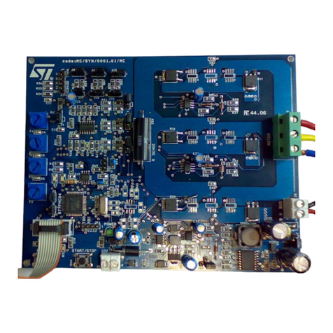
Figure 1. STEVAL-PTOOL2V1 evaluation board
Getting started with the STEVAL-PTOOL2V1 compact reference design for
medium voltage brushless power tools based on STSPIN32F0252
UM2772
User manual
UM2772 - Rev 1 - October 2020
For further information contact your local STMicroelectronics sales office.
www.st.com

1Getting started
1.1 Safety precautions
Danger:
There is danger of serious personal injury, property damage or death due to electrical shock and
burn hazards if the kit or components are improperly used or installed incorrectly.
Warning:
• The kit is not electrically isolated from the high-voltage supply AC-DC input.
• The evaluation board is directly linked to the mains voltage. No insulation is ensured
between the accessible parts and the high voltage. All measurement equipment must be
isolated from the mains before powering the board.
• When using an oscilloscope with the evaluation board, it must be isolated from the AC line.
This prevents shock from occurring as a result of touching any single point in the circuit, but
does NOT prevent shock when touching two or more points in the circuit.
Caution: During assembly, testing, and operation, the evaluation board poses several inherent hazards, including bare
wires, moving or rotating parts and hot surfaces.
All operations involving transportation, installation, use and maintenance must be performed by skilled technical
personnel who is familiar with the installation, use and maintenance of power electronic systems.
Work area safety
• The work area must be clean and tidy
• Do not work alone when boards are powered
• Protect the area against any unauthorized access by putting suitable barriers and signs
• A system architecture that supplies power to the evaluation board must be equipped with additional control
and protective devices in accordance with the applicable safety requirements (i.e., compliance with technical
equipment and accident prevention rules)
Electrical safety
• Remove power supply from the evaluation board and electrical loads before performing any electrical
measurement
• Arrange measurement setup, wiring and configuration paying attention to high voltage sections
• Once the setup is complete, power the board
Danger:
Do not touch the evaluation board when it is powered or immediately after it has been
disconnected from the voltage supply as several parts and power terminals containing potentially
energized capacitors need time to discharge, and heat-sinks and transformers may still be very
hot.
The kit is not electrically isolated from the AC-DC input.
Personal safety
• Always wear suitable personal protective equipment, such as insulating gloves and safety glasses
• Take adequate precautions and install the board preventing accidental touch
• Use protective shields, such as insulating box with interlocks
UM2772
Getting started
UM2772 - Rev 1 page 2/28
1.2 Overview
The STEVAL-PTOOL2V1 features:
• 20 to 72 VDC input voltage
• Up to 250 V high voltage rail (limited to 100 V by on-board components)
• Up to 19 Arms output current
•STSPIN32F0252 featuring:
– 250 V, 1 A 3-phase gate driver
– Smart shutdown OCP
– Cortex-M0 STM32
•STL130N8F7 MOSFET power stage with:
– VDS = 80 V
– RDS(on) max. = 3.6 mΩ
– 5x6 PowerFlat package
• Single shunt current sensing for:
– Sensored or sensorless 6-step algorithm
– Single shunt vector algorithm
• Digital Hall sensors and encoder input
• Plug-and-play thanks to the six-step firmware with Hall-effect sensor feedback
• Speed regulation through an external trimmer
• Heat-sink for the best power dissipation performance
• Fully protected:
– Thermal shutdown
– Undervoltage lockout
– Overcurrent protection
• Compact footprint (80 x 58 mm)
• Bus voltage sensing
• 12 V VCC and 3.3 V VDD supplies
• Serial wire debug (SWD) port for debugging/programming
• UART TX-RX interface
• Simple user interface with buttons and trimmer
• RoHS compliant
1.3 Hardware and software requirements
To use the STEVAL-PTOOL2V1 board, you need:
• a Windows (XP, Vista, 7, 8 or 10) PC
•ST-LINK debugger/programmer for STM32
•STSW-PTOOL2V1 firmware
• a three-phase brushless or PMSM motor with compatible current and voltage ranges
• External DC power supply
1.4 Evaluation board intended use
The STEVAL-PTOOL2V1 is intended for evaluation purposes only and must not be used for electrical installations
or machinery. Technical data and information concerning the power supply conditions should be strictly observed.
UM2772
Overview
UM2772 - Rev 1 page 3/28

1.5 Installing the board
• The installation and cooling down of the evaluation board must be in accordance with the specifications and
target application
• The motor drive converters must be protected against excessive strain. In particular, components should not
be bent or isolating distances altered during transportation or handling
• No contact must be made with other electronic components and contacts
• The evaluation board contains electrostatic sensitive components that could be damaged if used incorrectly
UM2772
Installing the board
UM2772 - Rev 1 page 4/28

2Hardware description and configuration
Figure 2. STEVAL-PTOOL2V1 circuitry main blocks - top view
1. SWD, UART, GPIOs
2. Power supply
3. Feedback network
4. STSPIN32F0252
1
2
3
4
UM2772
Hardware description and configuration
UM2772 - Rev 1 page 5/28

Figure 3. STEVAL-PTOOL2V1 circuitry main blocks - bottom view
1. Power stage
2. Shunt resistor
3. Heat sink mounting hole
4. Heat sink mounting hole
5. Heat sink mounting hole
6. Heat sink mounting hole
1
2
3
5
4
6
UM2772
Hardware description and configuration
UM2772 - Rev 1 page 6/28

Figure 4. STEVAL-PTOOL2V1 main components and connectors
1. J3 external trigger
2. VBAT-
3. VBAT+
4. J8 W phase
5. J7 V phase
6. J6 U phase
7. J2 Hall encoder connector
8. J1 external speed regulation potentiometer
9. TR1 speed regulation trimmer
10. SW1 spinning direction switch
11. J9 external direction switch
12. J10 UART SWD - GPIO connector
13. J11 SWD connector
14. SW2 trigger button
Table 1. Jumper settings
Jumper Permitted configurations Default condition
JP1 External reset (connected through soldering pads) OPEN
JP2 Selection PA0 connected to BEMF phase U (1-2 CLOSED) or Hall 1 (2-3 CLOSED) (2-3 CLOSED)
JP3 Selection PA1 connected to BEMF phase V (1-2 CLOSED) or Hall 2 (2-3 CLOSED) (2-3 CLOSED)
JP4 Selection PA2 connected to BEMF phase W (1-2 CLOSED) or Hall 3 (2-3 CLOSED) (2-3 CLOSED)
UM2772
Hardware description and configuration
UM2772 - Rev 1 page 7/28

Table 2. Connectors and test points
Name Pin Label Description
J1 1-2-3 J1 External potentiometer connector (remove R70 if used)
J2
1 A+/H1
Hall/encoder sensor connector2 B+/H2
3 Z+/H3
4 VDD
Hall sensor/encoder supply
5 GND
J3 1-2 J3 External trigger switch
J4 1 VBAT+ Battery positive terminal
J5 1 VBAT- Battery negative terminal
J6 1 OUT U
3-phase BLDC motor phases connectionsJ7 1 OUT V
J8 1 OUT W
J9 1-2-3 J9 External direction switch connector (remove R68 if used)
J10
1
J10
NRST – MCU reset
2 GND
3 SWDIO – MCU debug IO port
4 PB1 MCU GPIO
5 GND
6 PB0 MCU GPIO
7 SWCLK – MCU debug clock port
8 VBUS_fdbk (PA7) – Battery supply MCU monitor
9 VDD – MCU supply
10 CURRENT_REF (PA6) – current reference for 6-step current mode control
11 PA15 MCU GPIO
12 Curr_fdbk (PA5) – shunt current MCU sensing
13 PB3 MCU GPIO
14 Temp_fdbk (PA4) – Power bridge MCU monitor
15 UART1_TX (PB6) – MCU uart transmit
16 PA3 MCU GPIO – Speed set point MCU monitor
17 UART1_RX (PB7) – MCU UART receive
18 PF1 MCU GPIO
19 BOOT0 – MCU bootloader selector
20 PB8 MCU GPIO
J11
1 SWD IO
Auxiliary connector for SWD mode debugging/programming
2 SWD CLK
3 GND
UM2772
Hardware description and configuration
UM2772 - Rev 1 page 8/28

Table 3. Test points
Name Pin Label Description
TP1 - TP1 W phase high side gate
TP2 - OUT3 W phase
TP3 - TP3 RES3
TP4 - TP4 RES2
TP5 - TP5 W phase low side gate
TP6 - TP6 RES1
TP7 - TP7 SENSE
TP8 - TP8 PB4 MCU GPIO
TP9 - TP9 V phase high side gate
TP10 - TP10 V phase
TP11 - TP11 V phase low side gate
TP12 - TP12 SENSE
TP13 - TP13 Speed set point
TP14 - GND GND – signal ground
TP15 - PGND PGND – power ground
TP16 - TP16 PB5 GPIO
TP17 - OD OD – Smart SD Open Drain output, unlatch and restart input
TP18 - TP18 U phase high side gate
TP19 - TP19 U phase
TP20 - TP20 U phase low side gate
TP21 - TP21 SENSE
TP22 - TP22 CIN – comparator positive input
UM2772
Hardware description and configuration
UM2772 - Rev 1 page 9/28

3How to use the board
Step 1. Check the jumper position according to the target configuration (see Section 2 Hardware description
and configuration).
Step 2. Connect the motor phases to J6, J7 and J8 pads on the basis of the motor phase sequence.
Step 3. Supply the board through DC J4 (VBAT+) and J5 (VBAT-) pads.
Step 4. Develop your application using the STSW-PTOOL2V1 firmware example package as starting point.
3.1 Sensorless mode
To configure the STEVAL-PTOOL2V1 evaluation board for 6-step sensorless mode, BEMF network components
(R65, R66, R67) have to be mounted and the BEMF detection network must be enabled.
You have to set jumpers as follows:
• JP2 pins 1-2: closed, PA0 connected to BEMF phase U
• JP3 pins 1-2: closed, PA1 connected to BEMF phase V
• JP4 pins 1-2: closed, PA2 connected to BEMF phase W
UM2772
How to use the board
UM2772 - Rev 1 page 10/28

4Hall/encoder motor speed sensor
The STEVAL-PTOOL2V1 evaluation board supports the digital Hall and quadrature encoder sensors for motor
position feedback.
Sensors can be connected to the STSPIN32F0252 through J2 connector as listed in the following table.
Table 4. Hall/encoder sensors and J2 connections
Name Pin Description
Hall1/A+ 1 Hall sensor 1/encoder out A+
Hall2/B+ 2 Hall sensor 2/encoder out B+
Hall3/Z+ 3 Hall sensor 3/encoder Zero feedback
VHALL 4 Sensor supply voltage (default VDD)
GND 5 Ground
A protection resistor of 1 kΩ is mounted in series with sensor outputs.
For sensors requiring external pull-up, three 10 kΩ resistors are already mounted on the output lines and
connected to VDD voltage.
Set jumper resistors (R43 and R44) to configure the power supply for sensor supply voltage as follows:
• R44 mounted, R43 unmounted → Hall sensors powered by VDD (3.3 V)
• R44 unmounted, R43 mounted → Hall sensors powered by VCC (12 V)
The STSPIN32F0252 MCU can decode Hall/encoder sensor outputs by configuring jumpers as follows:
• JP2 pins 2-3: closed, PA0 connected to Hall1
• JP3 pins 2-3: closed, PA1 connected to Hall2
• JP4 pins 2-3: closed, PA2 connected to Hall3
UM2772
Hall/encoder motor speed sensor
UM2772 - Rev 1 page 11/28

5Overcurrent detection and current sensing measurement
The STEVAL-PTOOL2V1 evaluation board implements overcurrent protection based on the STSPIN32F0252
integrated comparator.
The single shunt resistor measures the load current bringing the voltage signal associated to the load current and
amplified by U2B OpAmp to CIN pin (TP22). When the phase peak current exceeds the selected threshold, the
integrated comparator is triggered and all power switches are disabled until the current falls below the threshold
and the output disable time expires.
Figure 5. Current sensing and disable time circuitry
PB0
47nF/20V
CIN
LVG1
VCC
PA6
Vocp
LVG2
R16
TP22
27
LVG2
29
VDD
22
PB0
20
PA5
17
TP17
PB1
OD
24
PB1
21
C10
23
GND
26
OD
CIN
LVG1
28
RES4
31
VDD
CIN
25
LVG3
30
47k
U1
VBUS_fdbk 18
PA7
19
VSS
LVG3
Output disable time circuitry
1.5k
IN-6
N.M.
C44
3.3nF/10V 1nF/10V
1.5k
R63
6.8k
100R
+
-
7
OUT
C41
N.M.
Vocp
R58
6.8k
ISNSP R621k
C43
R59
N.M.
R57
R56 U2B
ISNSN
100R
TSV912
5 IN+
C42
R61
R60
VDD
Current signal amplifying network
By default, the STEVAL-PTOOL2V1 evaluation board overcurrent threshold is set to IOC_typ = 36 A and the restart
time after fault detection is ~735 µs.
Overcurrent threshold can be modified by changing the amplifying circuit gain and offset, according to the
following formulas:
IOCtyp =VREFtyp ⋅1
5RSHUNT ⋅ Ra ⋅ G − VDD ⋅ Rb
RSHUNT ⋅ Ra (1)
Where, based on default values:
VREF_typ = 460 mV, VDD = 3.3 V, RSHUNT = R25 = 3 mΩ and
Ra =R63//R61
R56 + R58 + R63/ /R61 = 0.81 R63 + ∞(2)
Rb =R58 + R56 / /R61
R63 + R58 + R56 / /R61 = 0 R63 + ∞ G = 1 + R60
R58 + R56 = 5.25 (3)
Therefore:
IOCtyp ≅36 A
The output disable time can be monitored on OD pin (TP17) and is determined by the time required to recharge
C10 capacitor up to VSSDh threshold, according to:
VSSDh = 3.8 V, VSSDI = 0.56 V, VOD = VCC =12 V
T2≅ C10 ⋅ R16 ⋅1nVSSDl − VOD
VSSDℎ− VOD (4)
UM2772
Overcurrent detection and current sensing measurement
UM2772 - Rev 1 page 12/28

6Bus voltage circuit
The STEVAL-PTOOL2V1 evaluation board provides the bus voltage sensing. This signal is set through voltage
dividers (R71 and R72) from motor supply voltage (VBAT) and sent to PA7 GPIO (ADC channel 7) of the
embedded MCU. The default voltage divider is set to 24.3.
UM2772
Bus voltage circuit
UM2772 - Rev 1 page 13/28

7Hardware user interface
The STEVAL-PTOOL2V1 board provides a hardware user interface which consists of:
• a trimmer (TR1) to set the target speed
• SW1 switch to set motor spin direction
• SW2 switch to turn the board power supply on or off, thus reducing static consumption to 0 A via Q8 P-
channel MOSFET. If a continuous power supply is needed, for example, to load the firmware onto the MCU,
short J3 connector pins.
All above mentioned interfaces can be replaced by external inputs.
7.1 Detachable interface
If the on-board hardware user interface (SW1, SW2 and TR1) are not used, it is possible to detach the interface
section by breaking the PCB along the slot holes.
You can still program or debug STSPIN32F0252 by connecting an external ST-LINK/V2-1 to J11 SWD connector.
Figure 6. STEVAL-PTOOL2V1 detachable section
7.2 Turn on/off circuitry
The board offers the possibility of connecting or disconnecting the battery to the circuitry via an external switch
(J3), to reduce the quiescent consumption to a very low level.
As soon as the switch is closed, the motor can be driven as required by the control algorithm.
By closing the trigger switch, the Q8 PMOS gate is forced low, connecting the battery to the control circuitry.
UM2772
Hardware user interface
UM2772 - Rev 1 page 14/28

Figure 7. Turn on/off trigger circuitry
C29
1uF/100V
3
D19
BZT585B15T
4
Driver and logic power supply
1
R690R
J4
1
D20
BAT46JFILM
R50
10k
R51
10k
1
Q8
STN3P10F6
2
1
Q7
BSS123W
J3
N.M.
R48
10k
C30
1nF/100V
VBAT
3
2
R49
10k
J5
D24 BAT30
C46
N.M.
VDD
C28
1uF/100V
2
SW2
KSC7xxJ
1
3
2
1
GPIO input (trigger monitor)
GPIO output (keep-alive circuit)
7.2.1 Keep-alive circuit
As soon as the Q8 PMOS connects the battery to the buck regulator, the power-up sequence starts, and VCC and
VDD are provided to the STSPIN32F0252 driver and MCU, respectively.
When the MCU is operative, the PMOS can be kept turned on using Q7 NMOS, which acts as an MCU driven
switch in parallel with the external trigger switch. Thus, the firmware takes control of the connection between the
battery and the STSPIN32F0252 allowing the code to perform a safe switch-off (for example, by applying a brake
sequence to the motor).
Note: Set the GPIO output (PC14) HIGH at MCU initialization.
7.2.2 External trigger status detection
While the STSPIN32F0252 is supplied by the keep-alive circuit, the actual status of the external trigger switch
must be constantly monitored to execute the shutdown sequence when it is released.
The monitoring GPIO (PC15) is connected to the switch through D20 diode. As long as the switch is closed, the
GPIO is forced low through D20. Releasing the switch, D20 is no more polarized and the GPIO is pulled up by
R49 resistor. Therefore, setting an interrupt on the rising edge of PC15 allows detecting the trigger release and
stop the motor.
UM2772
Turn on/off circuitry
UM2772 - Rev 1 page 15/28

8Debug
The STEVAL-PTOOL2V1 evaluation board can be connected to an external ST-LINK/V2-1 debugger/programmer
which features:
• USB software re-enumeration
• Virtual COM port interface on USB connected to the STSPIN32F0252 (UART1) PB6/PB7 pins
• Mass storage interface on USB
The power supply for ST-LINK/V2-1 is provided by the host PC.
The MCU programming/debugging phase can be performed through the serial wire interface available on J10 or
J11 connectors.
UM2772
Debug
UM2772 - Rev 1 page 16/28

9Schematic diagrams
Figure 8. STEVAL-PTOOL2V1 circuit schematic (1 of 2)
SPEED
OD
OUT3
OUT2
OUT1
GND PGND
CIN
Potentiometer
OPEN
RESET
SWCLK
SWDIO
GND
NRST
TH P_2.54mm 2 rows
20 pins header
NOT POPULATED
SWD connector
UART1_TX
UART1_RX
VDD
VCC
VCC
VDD
VDDVDD
VDD
VDD
VCC
VCC
VCC
VDD VDD VDD
VCCVCC
VDD
VBAT
VBAT
VBAT
VBAT
VDD
VDD
VDD
VDD
VDD VBAT
P A0
P A1
P A2
P C1 4
P C1 5
OUTU
OUTV
OUTW
GP IO_ BEMF
ISNS N
ISNS P
Vocp
R2 8
0R
R2 2
22 R
TP 17
TP 9
Q6
1
4
5
2 3
6 7 8
C2 0
100nF/10V
J9
N.M.
1
2
3
J8
1
C1 1
1u F/50V
+
C1 9
220uF/100V
D1
S TP S 1H 100 MF
1 2
R2 0
4.7 R
C1 3
4.7 uF /10V
R7
27R
TP 15
+
-
U3
TS 86 1
4
3
5 1
2
Q2
1
4
5
2 3
6 7 8
C4 7
N.M.
D5
BAT54J
R7 0
0R
TP 21
D3
BAT54J
TP 8
R1 1
0R
Q5
1
4
5
2 3
678
Q4
1
4
5
2 3
6 7 8
D2
BAT54J
R5 5
1k
C1 8
100nF/10V
R6
22R
J P 1
R4 5
10 0k
C1
100nF/10V
TP 20
R6 4
4.7 k
S W1
J S 10 20 11 J CQ N
R4
4.7 R
R8
4.7 R
TP 10
TP 7
R2 7
0R
R1 8
22 R
TP 5
TP 13
R2 4
51k
C8
100nF/100V
R1 0
4.7 R
D1A
N.M.
R1 9
N.M.
C9
4.7nF/10V
TP 18
R2
4.7 R
D9
BAT54J
J6
1
C1 2
100nF/10V
R2 3
N.M.
R9
22 R
R1
27 R
R1 4
0R
C1 4
33 pF/10V
C1 0
47 nF/20V
NTC1
10 k 1%
12
TP 14
R1 5
27R
D4
S TP S 1H 100 MF
1 2
R6 8
0R
D25
BAT30
R3
22 R
C7
1uF/50V
R2 6
3k
R1 6
47k
Q3
1
4
5
2 3
6 7 8
D6
BAT54J
D4A
N.M.
TR1
100k
R7 1
91k
R2 5
3 mOhm-3W-1%
R7 2
3.9 k
J10
S TRIP 2x10
1
3
5
7
9
11
13
15
17
19
2
4
6
8
10
12
14
16
18
20
R2 9
33k
C5
100nF/20V
R1 3
1k
TP 11
1 2
C4
1uF/50V
D7
S TP S 1H 100 MF
1 2
TP 19
TP 12
Q1
1
4
5
2 3
6 7 8
U1
S TS P IN32F 02 52
P B8
1
VSS
2
VDD
3
P C1 3
4
P C1 4
5
P C1 5
6
P F0
7
P F1
8
NR S T
9
VDDA
11
P A0
12
P A1
13
P A2
14
P A3
15
P A4
16
P A5
17
P A6
18
P A7
19
P B1
21
OD
24
CIN
25
LVG1
28
LVG2
29
LVG3
30
HVG1 34
OUT1 3 3
BOOT1 35
OUT2 4 0
BOOT2 42
HVG2 41
OUT3 4 6
BOOT3 48
HVG3 47
RE S 1 52
RE S 2 53
RE S 3 54
P A12 55
P A13 56
P A14 57
P A15 58
P B3 59
P B4 60
P B5 61
P B6 62
VDD
22
EP AD 65
VSS A
10
P B0
20
VSS
23
GND
26
P GND
27
VCC 51
P B7 63
BOOT0 64
RE S 4
31
RE S 5 50
R5
0R
J1
N.M.
1
2
3
C1 5 N.M.
C1 6
100nF/10V
TP 2
C4 5
4.7 nF /10V
C3
100nF/10V
J7
1
C6
220nF/20V
C1 7
2.2nF/10V
J11
N.M.
1
2
3
D8
BAT54J
R1 2
22R
D7A
N.M.
TP 6
R3 0
10M
TP 16
+
-
U2A
TS V91 2
Vcc-
4
IN+3
IN-2
OUT 1
Vcc+
8
TP 1
TP 4
TP 22
C2
10 0nF/10V
1 2
R1 7
4.7 R
R2 1
3k
TP 3
VBUS _fdb k
CP O UT
CURRENT_REF
ISNS P
P B0
P B1
CURRENT_REF
CP O UT
UART1_TX
UART1_RX
P B8
S WDIO
S EN S E
LVG3
GH3
GL3
S EN S E
GH2
GL2
GH1
GL1
LVG1
LVG2
Cu rr_fdbk LVG3
LVG2
LVG1
NR S T
S EN S E
CIN
Cu rr_fdbk
P A3
P B5
P B4
P B3
P A15
P F1
OUTU
OUTV
OUTW
BOOT0
NR S T
P B3
UART1_RX
UART1_TX
S WDIO
S WCLK
P A15
NR S T
BOO T0P B8
ISNS N
Temp_fdbk
Temp_fdbk
S WCLK
VBUS _fdb k
P B1
Cu rr_fdbk
P A3
CURRENT_REF
P B0
Te mp _fdb k
P F1
DIRECTION
N15912968N15847582
N16912803
N16990454
N15848292
N15848824
STL130N8F7
STL130N8F7
STL130N8F7
STL130N8F7
STL130N8F7
STL130N8F7
UM2772 - Rev 1 page 17/28
UM2772
Schematic diagrams

Figure 9. STEVAL-PTOOL2V1 circuit schematic (2 of 2)
VHALL
Z+/H3
GND
A+/H1
B+/H2
VDD
VDD
VHALL
VCC VHALL VDD
VBAT ViDRAIN
VDD
VDD
ViDRAIN
VCC
VCC
VDD
VDD
VDD
OUTW
GP IO_ BEMF
OUTV
OUTU
P A0
P A1
P A2
P C 14
P C 15 IS NS P
IS NS N
Vocp
R58
1.5k
C40
10 uF /10 V
R62 1k
J P 4
13
2
R36
1k
C43 N.M.
C34
1n F/10V
Q7
BS S 1 23W
3
1
2
R53 82k
+
C38
68 uF /20 V
R59
1.5k
R34
1k
R40
1.5k
R39
N.M.
C44
1nF/10V
R42
1.5k
R50
10 k
C33
N.M.
U4 VIP e r01 3
COMP
5
GND 1
Vcc 2
DIS 3
FB 4
Drain
6
Drain
7
Drain
8
Drain
9
Drain
10
R31
10 k R65 33k
C24
100nF/20V
R52
9.1k
C36
1uF/50V
D18
BAT30
J3
N.M.
1
2
Q8
S TN3 P 10 F6
3
1
2
J4
1
S W2
KS C7 xxJ
1
2
3
4
J5
1
C32
220nF/20V
R63
N.M.
R69 0R
D10
BAT30
R56
100R
C30
1nF/100V
C37
10 0n F/50V
C23
100pF/10V
R57
100R
R66 33k
C46
N.M.
U5
LD11 17 S 33 CTR
Vout 2
GND
1
Vin
3
D21 BAT41Z
C29
1u F/100 V
D11
BAT30
R37
N.M.
D15
BZT585B3V3T
+
C31
22 uF /20 V
+
-
U2 B TS V91 2
IN+5
IN-6
OUT 7
R60 6.8k
R46
0R
R41
1.5k
R47
12k
C28
1uF/100V
C39
100nF/20V
R38
N.M.
C41
3.3nF/10V
R51
10k
D14
BZT585B3V3T
R32
10k
C42 N.M.
R43
N.M.
C35
1nF/50V
D17
BAT30
R61 6.8k
R48
10k
J2
1
2
3
4
5
R67 33k
D16
BAT30
R35
1k
D12
BAT30
R44
0R
D24 BAT30
L1 270 uH
1 2
D20
BAT46JFILM
J P 2
13
2
D13
BZT585B3V3T
C21
100pF/10V
R33
10k
D23
S TTH1 02 A
D19
BZT585B15T
J P 3
13
2
R54
2.7k D22
S TTH1 02 A
R49
10k
C22
10 0pF/10V
Z+/H3_C
B+/H2_C
A+/H1_C
P A2_ BEMF
P A1_ BEMF
P AO_BE MF
P AO_BE MF
P A1_ BEMF
P A2_ BEMF
UM2772 - Rev 1 page 18/28
UM2772
Schematic diagrams

10 Bill of materials
Table 5. STEVAL-PTOOL2V1 bill of materials
Item Q.ty Ref. Part/Value Description Manufacturer Order code
1 7
C1, C2, C3,
C12, C16,
C18, C20
100 nF/10
V/X7R 0603
SMT Ceramic
Capacitor Wurth Elektronik 885012206020 or
equivalent
2 4 C4, C7, C11,
C36
1 µF/50 V/X5R
0805
SMT ceramic
capacitor Wurth Elektronik 885012207103 or
equivalent
3 3 C5, C24, C39 100 nF/20
V/X7R 0603
SMT Ceramic
Capacitor Wurth Elektronik 885012206071 or
equivalent
4 2 C6, C32 220 nF/20
V/X7R 0603
SMT ceramic
capacitor Wurth Elektronik 885012206073 or
equivalent
5 1 C8 100 nF/100 V
1210
SMT Ceramic
Capacitor TDK CGA6M3X7R2E104M200A
E or equivalent
6 2 C9, C45 4.7 nF/10 V
0603
SMT Ceramic
Capacitor Wurth Elektronik 885012206012 or
equivalent
7 1 C10 47 nF/20 V/X7R
0603
SMT Ceramic
Capacitor Wurth Elektronik 885012206069 or
equivalent
8 1 C13 4.7 µF/10 V/
X7R0805
SMT Ceramic
Capacitor Wurth Elektronik 885012207025 or
equivalent
9 1 C14 33 pF/10 V/NPO
0603
SMT Ceramic
Capacitor Wurth Elektronik 885012006005 or
equivalent
10 6
C15, C33,
C42, C43,
C46, C47
N.M. 0603
SMT ceramic
capacitor (not
mounted)
Any
11 1 C17 2.2 nF/10 V/X7R
0603
SMT Ceramic
Capacitor Wurth Elektronik 885012206010 or
Equivalent
12 1 C19
220 µF/100 V
Diam. 12.5mm p.
5mm 100V
THT Electrolytic
Capacitor Panasonic EEUFS2A221B or
equivalent
13 3 C21, C22,
C23
100pF/10V/
X7R0603
SMT Ceramic
Capacitor Wurth Elektronik 885012206003 or
equivalent
14 2 C28, C29 1 µF/100V 1210 SMT ceramic
capacitor KEMET C1210C105K1RACAUTO
15 1 C30 1nF/100V/X7R
0805
SMT ceramic
capacitor Wurth Elektronik 885012207116 or
equivalent
16 1 C31 22 µF/20V 5x5.4
mm 20V
SMT Aluminum
Elect. Capacitor Wurth Elektronik 865090442004 or
equivalent
17 1 C34 1nF/10V/X7R
0603
SMT ceramic
capacitor Wurth Elektronik 885012206008 or
equivalent
18 1 C35 1 nF/50 V/X7R
0603
SMT ceramic
capacitor Wurth Elektronik 885012206083 or
equivalent
19 1 C37 100 nF/50 V/
X7R0805
SMT ceramic
capacitor Wurth Elektronik 885012207098 or
equivalent
20 1 C38 68 µF/20 V D / E
20V
Low ESR series
of robust MnO2
solid electrolyte
capacitors
AVX TPS Series or equivalent
21 1 C40 10 µF/10 V/X7R
1206
SMT Ceramic
Capacitor Wurth Elektronik 885012208018 or
equivalent
UM2772
Bill of materials
UM2772 - Rev 1 page 19/28

Item Q.ty Ref. Part/Value Description Manufacturer Order code
22 1 C41 3.3 nF/10 V/X7R
0603
SMT ceramic
capacitor Wurth Elektronik 885012206011 or
equivalent
23 1 C44 1 nF/10 V/NPO
0603
SMT ceramic
capacitor
24 3 D1, D4, D7
STPS1H100MF
STmite flat
(DO222-AA)
High voltage
power Schottky
rectifier
ST STPS1H100MF
N.M. SMA
High efficiency
ultrafast diode
(not mounted)
ST STTH102A
25 2 D22, D23 STTH102A SMA High efficiency
ultrafast diode ST STTH102A
26 6 D2, D3, D5,
D6, D8, D9
BAT54J
SOD-323
40 V, 300 mA
Small signal
Schottky SMT
Diode
ST BAT54JFILM
27 8
D10, D11,
D12, D16,
D17, D18,
D24, D25
BAT30 SOD-523
30 V, 300 mA
small signal
Schottky SMT
diode
ST BAT30KFILM
28 3 D13, D14,
D15
BZT585B3V3T
SOD523
Surface mount
precision Zener
diode
Diodes
Incorporated
BZX585B3V3T or
equivalent
29 1 D19 BZT585B15T
SOD523
Surface mount
precision Zener
diode
Diodes
Incorporated BZT585B15T or equivalent
30 1 D20 BAT46JFILM
SOD-323
100 V, 150 mA
small signal
Schottky diode
ST BAT46JFILM
31 1 D21 BAT41Z
SOD-123
100 V, 200 mA
low capacitance
small signal
Schottky diode
ST BAT41ZFILM
32 1 JP1 OPEN Soldering
pads SMT jumper Any
33 3 JP2, JP3, JP4 CLOSE 2-3
Soldering pads SMT jumper Any
34 3 J1, J9, J11 N.M. 1x3 pins
Strip connector 3
pos, 2.54 mm
(not mounted)
Wurth Elektronik 61300311121 or equivalent
35 1 J2 STRIP 1x5 1x5
pins
Strip connector 5
pos, 2.54 mm Wurth Elektronik 61300511121 or equivalent
36 1 J3 N.M. 1x2 pins
Strip connector 2
pos, 2.54 mm
(not mounted)
Wurth Elektronik 61300211121 or equivalent
37 2 J4, J5 N.M. Dim.
6.2x6.5 mm
Solder Pad (not
mounted) Any
38 3 J6, J7, J8 N.M. Dim.
6.2x6.5 mm
Solder Pad (not
mounted) Any
39 1 J10 STRIP 2x10
2x10 pins
Strip connector
2x10, pitch 2.54
mm
Wurth Elektronik 61302021121 or
Equivalent
UM2772
Bill of materials
UM2772 - Rev 1 page 20/28
Table of contents
Other ST Motherboard manuals

ST
ST EVAL-L9963E-MCU User manual

ST
ST STM32L1 Series Installation and operating instructions

ST
ST STEVAL-1PS03A User manual

ST
ST EVALSP1340CPU User manual

ST
ST EVAL-L99DZ200 User manual

ST
ST STM32 Nucleo-64-P Series User manual

ST
ST UM1461 User manual

ST
ST Nucleo STM32F302R8 User manual

ST
ST STEVAL-IHM020V1 User manual

ST
ST EVALSTPM34 User manual