ST NUCLEO-8S207K8 User manual

Introduction
The NUCLEO-8S207K8 STM8 Nucleo-32 board featuring the STM8S207K8T6C STM8 8-bit MCU provides an affordable and
flexible way for users to try out new concepts and build prototypes with STM8S Series microcontrollers in LQFP32 package,
choosing from the various combinations of performance, power consumption, and features. The ARDUINO® Nano connectivity
support makes it easy to expand the functionality of the Nucleo-32 open development platform with a wide choice of specialized
shields. The STM8 Nucleo-32 board does not require any separate probe as it integrates the ST-LINK/V2-1 debugger/
programmer and comes with the STM8 standard peripheral library, together with various packaged software examples.
Figure 1. NUCLEO-8S207K8 top view Figure 2. NUCLEO-8S207K8 bottom view
Pictures are not contractual.
STM8 Nucleo-32 board (MB1442)
UM2391
User manual
UM2391 - Rev 1 - November 2019
For further information contact your local STMicroelectronics sales office.
www.st.com

1Features
• STM8 microcontroller in LQFP32 32-pin package
• 4 LEDs:
– USB communication (LD1)
– Power (LD2)
– User (LD3)
– Default (LD4)
• 1 reset push-button
• Board connectors:
–ARDUINO® Nano V3 expansion connector
– Micro-B USB connector for the ST-LINK
– SWIM interface
• Flexible power-supply options: ST-LINK USB VBUS or external sources (3.3 V, 5 V, 7 V – 12 V)
• On-board ST-LINK/V2-1 debugger/programmer with SWIM connector and USB re-enumeration capability:
mass storage, Virtual COM port and debug port
• Comprehensive free software STM8 libraries including a variety of software examples
• Support of a wide choice of Integrated Development Environments (IDEs) including STMicroelectronics free
STVD-STM8 (using Cosmic toolchain), IAR™, Cosmic free IDEA
UM2391
Features
UM2391 - Rev 1 page 2/25

2Ordering information
To order the STM8 Nucleo-32 board, refer to Table 1. Additional information is available from the datasheet and
reference manual of the target STM32.
Table 1. Ordering information
Order code Board reference Target STM32
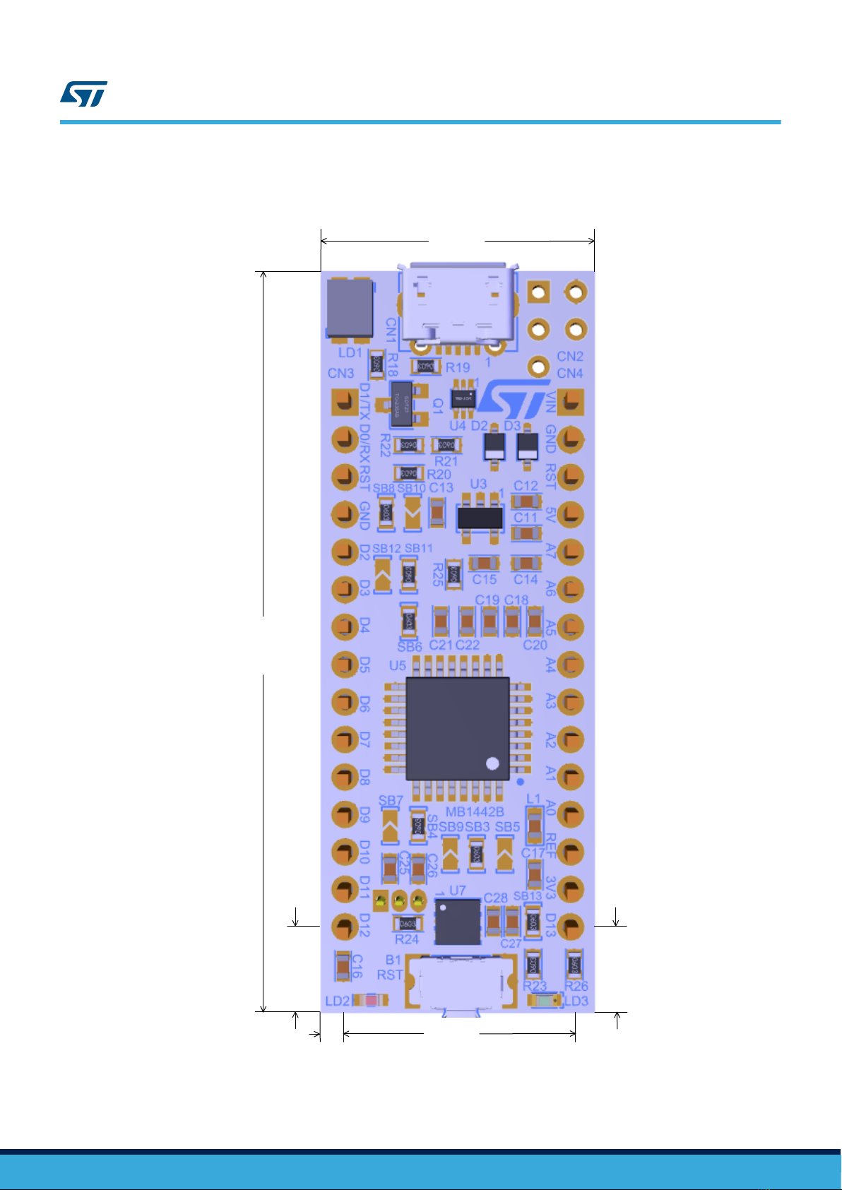
NUCLEO-8S207K8 MB1442 STM8S207K8T6C
2.1 Product marking
Evaluation tools marked as “ES” or “E” are not yet qualified and therefore not ready to be used as reference
design or in production. Any consequences deriving from such usage will not be at ST charge. In no event, ST will
be liable for any customer usage of these engineering sample tools as reference designs or in production.
“E” or “ES” marking examples of location:
• On the targeted STM8 that is soldered on the board (for illustration of STM8 marking, refer to the STM8
datasheet “Package information” paragraph at the www.st.com website).
• Next to the evaluation tool ordering part number that is stuck or silk-screen printed on the board.
2.2 Codification
The meaning of the codification is explained in Table 2.
Table 2. Codification explanation
NUCLEO-XXYYYKT Description Example: NUCLEO-8S207K8
XX MCU series in STM8 8-bit MCUs STM8S Series
YYY MCU product line in the series STM8S207
K STM8 package pin count 32 pins
T
STM8 Flash memory size:
• 3 for 256 bytes
• 4 for 16 Kbytes
• 6 for 32 Kbytes
• 8 for 64 Kbytes
• B for 128 Kbytes
64 Kbytes
The order code is mentioned on a sticker placed on the top side of the board.
UM2391
Ordering information
UM2391 - Rev 1 page 3/25

3Development environment
3.1 System requirements
• Windows® OS (7, 8 and 10)
• USB Type-A to Micro-B cable
3.2 Development toolchains
• STMicroelectronics: free STVD-STM8 (using Cosmic toolchain)
• IAR™: IAR-EWSTM8
• Cosmic: free IDEA
3.3 Demonstration software
The demonstration software is preloaded in the STM8 Flash memory for easy demonstration of the device
peripherals in standalone mode. The latest versions of the demonstration source code and associated
documentation can be downloaded from the demonstration resource section of the STM8 Nucleo board webpage
at www.st.com.
UM2391
Development environment
UM2391 - Rev 1 page 4/25

4Conventions
Table 3 provides the conventions used for the ON and OFF settings in the present document.
Table 3. ON/OFF convention
Convention Definition
Jumper JPx ON Jumper fitted
Jumper JPx OFF Jumper not fitted
Jumper JPx [1-2] Jumper should be fitted between Pin 1 and Pin 2
Solder bridge SBx ON SBx connections closed by 0 Ω resistor
Solder bridge SBx OFF SBx connections left open
Resistor Rx ON Resistor soldered
Resistor Rx OFF Resistor not soldered
UM2391
Conventions
UM2391 - Rev 1 page 5/25

5Quick start
The NUCLEO-8S207K8 STM8 Nucleo-32 board featuring the STM8S207K8T6C STM8 8-bit MCU provides an
affordable and flexible way for users to try out new concepts and build prototypes with an STM8S Series
microcontroller in an LQFP32 package.
Before installing and using the product, accept the Evaluation Product License Agreement from the www.st.com/
epla webpage.
For more information on the STM8 Nucleo-32 board and to access demonstration software, visit the www.st.com
webpage.
5.1 Getting started
1. Check jumper position onboard: JP1 (VDD) on [1-2] or [2-3] position.
2. Connect the STM8 Nucleo board to a PC with a Type-A to Micro-B USB cable through the USB connector
CN1 to power the board. Then LED LD1 (COM) and red LED LD2 (PWR) light up, the green LED LD3
blinks.
3. Remove the jumper placed between D2 (CN3 pin 5) and GND (CN3 pin 4).
4. Observe how the blinking of green LED LD3 changes when the jumper is in place or removed.
5. Download the demonstration software and several examples that help to use the STM8 Nucleo features.
These are available at the NUCLEO-8S207K8 product webpage.
6. Develop your own applications using the provided examples.
UM2391
Quick start
UM2391 - Rev 1 page 6/25

6Hardware layout and configuration
The STM8 Nucleo-32 board is designed around an STM8S Series microcontroller in an LQFP32 package.
Figure 3 shows the connections between the STM8 and its peripherals (ST-LINK/V2-1, push-button, LED, and
ARDUINO® Nano V3 expansion connector).
Figure 4 and Figure 5 show the location of these features on the STM8 Nucleo-32 board.
The mechanical dimensions of the board are shown in Figure 6.
Figure 3. Hardware block diagram
Embedded
ST-LINK/V2-1
STM8
Microcontroller
RESET
Micro
USB
IO IO
B1
RST
ARDUINO®
Nano connector
LED
LD3
ARDUINO®
Nano connector
UM2391
Hardware layout and configuration
UM2391 - Rev 1 page 7/25

6.1 STM8 Nucleo-32 board layout
Figure 4. STM8 Nucleo-32 board top layout
B1
Reset button
SB5
connects
OSCIN / PA1 to MCO
U5
STM8
microcontroller
U3
3V3 regulator
CN2
ST-LINK SWD
connector (reserved)
CN1
ST-LINK Micro-B
USB connector
LD3
Green LED
LD1
(Red/Green LED)
COM
SB8
connects
STM8 pin PD7 to TLI
SB4
connects
VCP RX to ST-LINK
SB3
connects
VCP TX to ST-LINK
LD2
Red LED Power
UM2391
STM8 Nucleo-32 board layout
UM2391 - Rev 1 page 8/25

Figure 5. STM8 Nucleo-32 board bottom layout
JP1
VDD select
SB2
RST mode of STM8
SB1
Power configuration
LD4
Default LED
CN4
ARDUINO®
Nano connector
CN3
ARDUINO®
Nano connector
U6
5V regulator
UM2391
STM8 Nucleo-32 board layout
UM2391 - Rev 1 page 9/25

6.2 Mechanical drawing
Figure 6. STM8 Nucleo-32 board mechanical drawing (in millimeter)
5.84 mm
5.84 mm
1.65 mm
15.24 mm
50.29 mm
18.54 mm
UM2391
Mechanical drawing
UM2391 - Rev 1 page 10/25

6.3 Embedded ST-LINK/V2-1
The ST-LINK/V2-1 programming and debugging tool is integrated into the STM8 Nucleo-32 board.
For detailed information about the debugging and programming features of ST-LINK/V2-1, refer to the ST-LINK/V2
in-circuit debugger/programmer for STM8 and STM32 user manual (UM1075) and Overview of ST-LINK
derivatives technical note (TN1235).
Features supported by the ST-LINK/V2-1:
• USB software re-enumeration
• Virtual COM port interface on USB
• Mass storage interface on USB
• USB power management request for more than 100 mA power on USB
Features not supported on ST-LINK/V2-1:
• SWIM interface
The embedded ST-LINK/V2-1 is directly connected to the SWIM port of the target STM8.
6.3.1 Drivers
The ST-LINK/V2-1 requires a dedicated USB driver, which, for Windows 7®, Windows 8® and Windows 10®, is
found at www.st.com.
In case the STM8 Nucleo-32 board is connected to the PC before the driver is installed, some STM8 Nucleo-32
interfaces may be declared as “Unknown” in the PC device manager. In this case, the user must install the
dedicated driver files, and update the driver of the connected device from the device manager as shown in
Figure 7.
Note: Prefer using the USB Composite Device handle for a full recovery.
Figure 7. USB composite device
6.3.2 ST-LINK/V2-1 firmware upgrade
The ST-LINK/V2-1 embeds a firmware mechanism for the in-situ upgrade through the USB port. As the firmware
may evolve during the lifetime of the ST-LINK/V2-1 product (for example new functionalities, bug fixes, support for
new microcontroller families), it is recommended to visit the www.st.com website before starting to use the STM8
Nucleo-32 board and periodically, to stay up-to-date with the latest firmware version.
UM2391
Embedded ST-LINK/V2-1
UM2391 - Rev 1 page 11/25

6.4 Power supply and power selection
The power supply is provided either by the host PC through the USB cable, or by an external source: VIN (7 V-12
V), 5V or 3V3 power supply pins on CN4. In case VIN, 5V or 3V3 is used to power the STM8 Nucleo-32 board,
this power source must comply with the standard EN-60950-1: 2006+A11/2009, and must be Safety Extra Low
Voltage (SELV) with limited power capability.
The MCU power supply is also selectable: 3V3 or 5V.
6.4.1 Power supply input from the USB connector
The STM8 Nucleo-32 board and shield board can be powered from the ST-LINK USB connector CN1. Note that
only the ST-LINK part is power supplied before the USB enumeration phase, as the host PC only provides 100
mA to the boards at that time. During the USB enumeration, the STM8 Nucleo-32 board requires 300 mA of
current to the host PC. If the host is able to provide the required power, the targeted STM8 microcontroller is
powered and the red LED LD2 is turned on, thus the STM8 Nucleo-32 board and its shield consume a maximum
of 300 mA current and not more. If the host is not able to provide the required current, the targeted STM8
microcontroller and the shield board are not power supplied. As a consequence, the red LED LD2 stays turned
off. In such a case, it is mandatory to use an external power supply as explained in the next Section
6.4.2 External Power supply inputs.
SB1 is configured according to the maximum current consumption of the board. SB1 can be set to ON to inform
the host PC that the maximum current consumption does not exceed 100 mA (even when ARDUINO® Nano
shield is plugged). In such a condition, USB enumeration always succeeds since no more than 100 mA is
requested to the host PC. Possible configurations of SB1 are summarized in Table 4.
Table 4. SB1 configuration
Solder bridge state(1) Power supply Maximum current
SB1 OFF
USB power through CN1
300 mA
SB1 ON 100 mA
1. The default configuration is reported in bold style.
Caution: If the maximum current consumption of the STM8 Nucleo-32 board and its shield board exceeds 300 mA, it is
mandatory to power the STM8 Nucleo-32 board, using an external power supply connected to VIN, 5V or 3V3.
Note: In case the board is powered by a USB charger, there is no USB enumeration, so the LED LD2 remains set to
off permanently and the target STM8 is not powered. In this specific case, the SB1 must be set to ON, to allow
the target STM8 to be powered anyway.
UM2391
Power supply and power selection
UM2391 - Rev 1 page 12/25

6.4.2 External Power supply inputs
The STM8 Nucleo-32 board and its shield boards can be powered in three different ways from an external power
supply, depending on the voltage used. The three power sources are summarized in Table 5.
Table 5. External power sources
Input
power
name
Connector pins Voltage range Max.
current Limitation
VIN CN4 pin 1 7 to 12 V 800 mA
From 7 to 12 V only and input current capability is linked to input
voltage:
• 800 mA input current when VIN = 7 V
• 450 mA input current when 7 V < VIN < 9 V
• 300 mA input current when 9 V < VIN < 10 V
• Less than 300 mA input current when 10 V < VIN
5V CN4 pin 4 4.75 to 5.25 V 500 mA ST-LINK not powered
3V3 CN4 pin 14 3.0 to 3.6 V - ST-LINK not powered and SB13 must be OFF.
VIN or 5V power supply
When powered from VIN or 5V, it is still possible to use ST-LINK for communication for programming or
debugging only, but it is mandatory to power the board first, using VIN or 5V, then to connect the USB cable to the
PC. In this way, the enumeration always succeeds, thanks to the external power source.
The following power sequence procedure must be respected:
1. Check that SB1 is OFF
2. Connect the external power source to VIN or 5V
3. Power on the external power supply 7 V < VIN < 12 V to VIN, or 5V
4. Check red LED LD2 is turned ON
5. Connect the PC to USB connector CN1
If this order is not respected, the board may be powered by VBUS first, then by VIN or 5V, and the following risks
may be encountered:
1. If more than 300 mA current is needed by the board, the PC may be damaged or current supplied is limited
by the PC. As a consequence, the board is not powered correctly.
2. 300 mA is requested at enumeration (since SB1 must be off) so there is the risk that the request is rejected
and the enumeration does not succeed if the PC cannot provide such current. Consequently, the board is
not power supplied (LED LD2 remains OFF).
3V3 power supply
When the board is powered by 3V3 (CN4 pin 14), the solder bridge SB13 must be OFF.
Using the 3V3 (CN4 pin 14) directly as power input can be interesting, for instance, in case the 3.3 V is provided
by a shield board. In this case, the ST-LINK is not powered, thus programming and debugging features are not
available.
In addition, to ensure powering the MCU, JP1 must be set to position [1-2].
6.4.3 External Power supply output
When powered by USB or VIN, the 5V (CN4 pin 4) can be used as an output power supply for an ARDUINO®
Nano shield. In this case, the maximum current of the power source specified in Table 5. External power sources
must be respected.
The 3.3V (CN4 pin 14) can be used also as a power supply output. The current is limited by the maximum current
capability of the regulator U7 (500 mA max).
UM2391
Power supply and power selection
UM2391 - Rev 1 page 13/25

6.4.4 MCU power selection
JP1, VDD choice, selects the power supply of MCU in 3V3 or 5V:
• 3V3: Connect the jumper between pin 1 and 2 of JP1
• 5V: Connect the jumper between pin 2 and 3 of JP1
It is possible to measure the STM32 microcontroller consumption by removing the jumper and connecting an
ammeter:
• Ammeter connected between [1-2]: power consumption measurement for VDD= 3V3
• Ammeter connected between [2-3]: power consumption measurement for VDD= 5V
6.5 LEDs
The tricolor LED (green, orange, red) LD1 (COM) provides information about ST-LINK communication status. The
LD1 default color is red. LD1 turns to green to indicate that the communication is in progress between the PC and
the ST-LINK/V2-1, with the following setup:
• Slow blinking red/OFF: at power-on before USB initialization
• Fast blinking red/OFF: after the first correct communication between PC and ST-LINK/V2-1 (enumeration)
• Red ON: when initialization between PC and ST-LINK/V2-1 is completed
• Green ON: after a successful target communication initialization
• Blinking red/green: during communication with the target
• Green ON: communication finished and successful
• Orange ON: communication failure
User LD3: The green LED is a user LED connected to the CN4 connector pin 15 (D13).
• When the I/O is HIGH value, the LED is ON
• When the I/O is LOW, the LED is OFF
PWR LD2: the red LED indicates that the STM8 part is powered and 5V power is available.
Default LD4: the red LED is a default LED connected to U2. It indicates that the current has exceeded the
expected limit.
6.6 Push-button
B1 RESET: the push-button is connected to NRST, and it is used to reset the STM8.
6.7 UART Virtual communication
Thanks to SB3 and SB4, the UART interface of STM8 available on PD5 (TX) and PD6 (RX), can be connected to
ST-LINK/V2-1. When UART Virtual communication is not used it is possible to use PD5/PD6 on ARDUINO® CN3
pins D1/D0. Refer to Table 6.
Table 6. Virtual communication configuration
Solder bridge State(1) Description
SB3
ON UART virtual communication enabled
OFF No UART virtual communication
SB4
ON UART virtual communication enabled
OFF No UART virtual communication
1. The default configuration is reported in bold style.
UM2391
LEDs
UM2391 - Rev 1 page 14/25

6.8 Solder bridge configuration
Table 7 details the solder bridges of the STM8 Nucleo-32 board.
Table 7. Solder bridge configuration
Bridge Setting(1) Description
SB1
ON USB power through CN1 allowed (100 mA max)
OFF USB power through CN1 allowed (300 mA max)
SB2
ON STM8 forced in a Reset mode
OFF STM8 not forced in a Reset mode (standard operation)
SB3, SB4 (ST-LINK-UART)
ON
PA2 and PA3 on STM32F103CBT6 (ST-LINK MCU) are connected
respectively to PD5 and PD6 on STM8 to have UART virtual
communication enabled. Thus SB7 and SB9 must be OFF.
OFF
PA2 and PA3 on STM32F103CBT6 (ST-LINK MCU) are disconnected
from respectively PD5 and PD6 on STM8. PD5 and PD6 can be used
as GPIO on Arduino connector CN4.
SB5
ON MCO on STM32F103CBT6 (ST-LINK MCU) is connected to PA1 on
STM8.
OFF MCO on STM32F103CBT6 (ST-LINK MCU) is disconnected from
PA1 on STM8.
SB6
ON GND is connected to AGND.
OFF GND is not connected to AGND.
SB7, SB9
ON T_VCP_TX and T_VCP_RX are connected to CN3.
OFF T_VCP_TX and T_VCP_RX are disconnected from CN3.
SB8
ON STM8 PD7 is connected to CN4 pin 5 for TLI support on
ARDUINO® Nano A7.
OFF STM8 PD7 is disconnected to CN4 pin 5 for TLI support on ARDUINO®
Nano A7.
SB10
ON STM8 PF4 is connected to CN4 pin 5 for AI12 support on ARDUINO®
Nano A7.
OFF STM8 PF4 is disconnected from CN4 pin 5 for AI12 support on
ARDUINO® Nano A7.
SB11
ON STM8 PF4 is connected to CN4 pin 6 for AI12 support on
ARDUINO® Nano A6.
OFF STM8 PF4 is disconnected from CN4 pin 6 for AI12 support on
ARDUINO® Nano A6.
SB12
ON STM8 PD7 is connected to CN4 pin 6 for TLI support on ARDUINO®
Nano A6.
OFF STM8 PD7 is disconnected from CN4 pin 6 for TLI support on
ARDUINO® Nano A6.
SB13
ON Output of voltage regulator LD39050PU33R is connected to 3.3V.
OFF Output of voltage regulator LD39050PU33R is not connected.
1. The default configuration is reported in bold style.
UM2391
Solder bridge configuration
UM2391 - Rev 1 page 15/25

6.9 ARDUINO® Nano connectors
CN3 and CN4 are male connectors compatible with ARDUINO® Nano standard. Most shields designed for
ARDUINO® Nano can fit the STM8 Nucleo-32 board
Caution: The STM8 I/Os are 3.3 V compatible instead of 5 V for ARDUINO® Nano.
Figure 8. ARDUINO® Nano connectors
VIN
GND
NRST
+5V
PD7 || PF4
PF4 || PD7
PB4
PB5
PB3
PB2
PB1
PB0
AREF
+3V3
PC5
PD5
PD6
NRST
GND
PD0
PC1
PD2
PC2
PC3
PA1
PA2
PC4
PE5 / PD4
PC6 / PD3
PC7
NUCLEO-8S207K8
1
2
3
4
5
6
7
8
9
10
11
12
13
14
15
1
2
3
4
5
6
7
8
9
10
11
12
13
14
15
D1
D0
RESET
GND
D2
D3
D4
D5
D6
D7
D8
D9
D10
D11
D12
VIN
GND
RESET
+5V
A7
A6
A5
A4
A3
A2
A1
A0
AREF
+3V3
D13
CN3 CN4
ARDUINO®
UM2391
ARDUINO® Nano connectors
UM2391 - Rev 1 page 16/25

Table 8 shows the ARDUINO® Nano connector pin assignment on the STM8 Nucleo-32 board.
Table 8. ARDUINO® Nano connectors on the STM8 Nucleo-32 board
Connector Pin number Pin name STM8 pin Function
Left connector
CN3
1 D1 PD5 UART3_TX(1)(2)
2 D0 PD6 UART_RX(1)(2)
3 RESET NRST RESET
4 GND - Ground
5 D2 PD0 TIM3_CH2
6 D3 PC1 TIM1_CH1
7 D4 PD2 TIM3_CH1
8 D5 PC2 TIM1_CH2
9 D6 PC3 TIM1_CH3
10 D7 PA1 -
11 D8 PA2 -
12 D9 PC4 TIM1_CH4
13 D10 PE5 / PD4 SPI_NSS / TIM2_CH1
14 D11 PC6 / PD3 SPI_MOSI / TIM2_CH2
15 D12 PC7 SPI_MISO
Right connector
CN4
1 VIN - Power input
2 GND - Ground
3 RESET NRST RESET
4 +5V - -
5 A7 PD7 | | PF4 TLI | | Analog input 12(1)
6 A6 PF4 | | PD7 Analog input 12 | | TLI
7 A5 PB4 Analog input 4 | | I2C_SCL
8 A4 PB5 Analog input 5 | | I2C_SDA
9 A3 PB3 Analog input 3
10 A2 PB2 Analog input 2
11 A1 PB1 Analog input 1
12 A0 PB0 Analog input 0
13 AREF - VDDA
14 +3V3 - 3.3 V I/O
15 D13 PC5 SPI clock
1. SB not fitted
2. In order not to have any conflict on the VCP signals (PD5 and PD6) when SB7 and SB9 are ON, SB3 and SB4 of ST-LINK
must be OFF. Conversely for the other case.
UM2391
ARDUINO® Nano connectors
UM2391 - Rev 1 page 17/25

7Federal Communications Commission (FCC) and Industry Canada
(IC) Compliance Statements
7.1 FCC Compliance Statement
Part 15.19
This device complies with Part 15 of the FCC Rules. Operation is subject to the following two conditions: (1) this
device may not cause harmful interference, and (2) this device must accept any interference received, including
interference that may cause undesired operation.
Part 15.21
Any changes or modifications to this equipment not expressly approved by STMicroelectronics may cause
harmful interference and void the user's authority to operate this equipment.
Part 15.105
This equipment has been tested and found to comply with the limits for a Class A digital device, pursuant to part
15 of the FCC Rules. These limits are designed to provide reasonable protection against harmful interference
when the equipment is operated in a commercial environment. This equipment generates, uses, and can radiate
radio frequency energy and, if not installed and used in accordance with the instruction manual, may cause
harmful interference to radio communications. Operation of this equipment in a residential area is likely to cause
harmful interference in which case the user will be required to correct the interference at his own expense.
Responsible party (in the USA)
Terry Blanchard
Americas Region Legal | Group Vice President and Regional Legal Counsel, The Americas
STMicroelectronics, Inc.
750 Canyon Drive | Suite 300 | Coppell, Texas 75019
USA
Telephone: +1 972-466-7845
7.2 IC Compliance Statement
Industry Canada ICES-003 Compliance Label: CAN ICES-3 (A) / NMB-3 (A).
UM2391
Federal Communications Commission (FCC) and Industry Canada (IC) Compliance Statements
UM2391 - Rev 1 page 18/25

8CE conformity
8.1 Warning
EN 55032 / CISPR32 (2012) Class A product
Warning: this device is compliant with Class A of EN55032 / CISPR32. In a residential environment, this
equipment may cause radio interference.
Avertissement : cet équipement est conforme à la Classe A de la EN55032 / CISPR 32. Dans un environnement
résidentiel, cet équipement peut créer des interférences radio.
UM2391
CE conformity
UM2391 - Rev 1 page 19/25

Revision history
Table 9. Document revision history
Date Version Changes
14-Nov-2019 1 Initial release
UM2391
UM2391 - Rev 1 page 20/25
This manual suits for next models
2
Table of contents
Other ST Motherboard manuals

ST
ST STEVAL-BLUEMIC-1 User manual

ST
ST STM32L073Z-EVAL User manual

ST
ST UM1789 User manual

ST
ST EVALSPEAr320PLC User manual

ST
ST STLINK-V3SEGT User manual

ST
ST SPC560D-DIS User manual

ST
ST STEVAL-SP1ML915 User manual

ST
ST STM32 Nucleo Installation and operating instructions

ST
ST STM32F746G-DISCO User manual

ST
ST FDA803S User manual

ST
ST AN3954 Installation and operating instructions

ST
ST STM32429I-EVAL1 User manual

ST
ST SPC58XXMB User manual

ST
ST STUSB02E User manual

ST
ST STEVAL-BTDP1 User manual

ST
ST STEVAL-USBPD45H User manual

ST
ST Contiki6LP User manual

ST
ST STEVAL-IHM015V1 User manual

ST
ST STM8S User manual

ST
ST STEVAL-IDB011V1 User manual