ST STEVAL-IPMM10B User manual

Introduction
The STEVAL-IPMM10B is a compact motor drive power board equipped with SLLIMM™ (small low-loss intelligent molded
module) 2nd series based on n-channel power MOSFET MDmesh™ DM2 fast-recovery diode (STIB1060DM2T-L). It provides
an affordable and easy-to-use solution for driving high power motors for a wide range of applications such as power white
goods, air conditioning, compressors, power fans, high-end power tools and 3-phase inverters for motor drives in general. The
IPM itself consists of MOSFETs and a wide range of features like undervoltage lockout, smart shutdown, embedded
temperature sensor and NTC, and overcurrent protection.
The main characteristics of this evaluation board are small size, minimal BOM and high efficiency. It consists of an interface
circuit (BUS and VCC connectors), bootstrap capacitors, snubber capacitor, hardware short-circuit protection, fault event and
temperature monitoring. In order to increase the flexibility, it is designed to work in single- or three-shunt configuration and with
double current sensing options such as using three dedicated onboard op-amps, or op-amps embedded in the MCU. The Hall/
Encoder part completes the circuit.
Thanks to these advanced characteristics, the system has been specifically designed to achieve fast and accurate current
feedback conditioning, satisfying the typical requirements for field-oriented control (FOC).
The STEVAL-IPMM10B is compatible with ST's STM32-based control board, enabling designers to build a complete platform for
motor control.
Figure 1. SLLIMM 2nd series motor control internal demo
board (top view)
Figure 2. SLLIMM 2nd series motor control internal demo
board (bottom view)
1200 W motor control power board based on STIB1060DM2T-L SLLIMM™ 2nd
series MOSFET IPM
UM2702
User manual
UM2702 - Rev 1 - April 2020
For further information contact your local STMicroelectronics sales office.
www.st.com

1Key features
• Input voltage: 125 - 400 VDC
•Nominal power: up to 1200 W
– Allowable maximum power is related to the application conditions and cooling system
• Nominal current: up to 4.2 Arms
• Input auxiliary voltage: up to 20 V DC
• Single- or three-shunt resistors for current sensing (with sensing network)
• Two options for current sensing: dedicated op-amps or through MCU
• Overcurrent hardware protection
• IPM temperature monitoring and protection
• Hall sensor or encoder input
• MOSFET intelligent power module:
– SLLIMM™ 2nd series IPM (STIB1060DM2T-L - DBC package)
• Motor control connector (32-pin) to interface with ST MCU boards
• Universal conception for further evaluation with breadboard and testing pins
• Very compact size
• WEEE compliant
• RoHS compliant
UM2702
Features
UM2702 - Rev 1 page 2/34

2Circuit schematics
The full schematics for the SLLIMM™ 2nd series card for STIB1060DM2T-L IPM products is shown below. This
card consists of an interface circuit (BUS and VCC connectors), bootstrap capacitors, snubber capacitor,
shortcircuit protection, fault output circuit, temperature monitoring, single-/three-shunt resistors and filters for input
signals. It also includes bypass capacitors for VCC and bootstrap capacitors. The capacitors are located very
close to the drive IC to avoid malfunction due to noise.
Dual current sensing options are provided: three dedicated on-board op-amps or embedded MCU op-amps;
selection is performed through three jumpers.
The Hall/Encoder section (powered at 5 V or 3.3 V) completes the circuit.
UM2702
Circuit schematics
UM2702 - Rev 1 page 3/34

2.1 Schematic diagrams
Figure 3. STEVAL-IPMM10B board schematic (1 of 5)
Input
DC_ bus _vo lta ge
STEVAL-IPMlnmx decoder
N
M
X
L
3.3V
+Bus 3.3V
1.65V
Bus _vo lta ge
RC6
0
RC2
0
RC12
0
D1
BAT48J FILM
RC1
0
+
C4
47u/35V
RC13
0
J1
INPUT-dc
1
2
RC10
0
RC7
0
R2
470K
R3 120R
R1
470K
R6
1k0
-
+
U1D
TSV994
12
13
14
411
RC3
0
RC8
0
RC4
0
+
C3
47u/35V
R4
7k5
C2
10n
RC5
0
RC9
0
RC11
0
+
C1
1000u/400V
R5
1k0
UM2702 - Rev 1 page 4/34
UM2702
Schematic diagrams

Figure 4. STEVAL-IPMM10B board schematic (2 of 5)
pha s e _A
pha s e _B
pha s e _C
3.3V
+5V
EM_S TOP
PWM-A-H
PWM-A-L
PWM-B-H
PWM-B-L
PWM-C-H
PWM-C-L
NTC_ byp a s s _re la y
P WM_Vre f
M_ pha s e _ A
M_ pha s e _ B
Bus _volta ge
M_ pha s e _ C
TS O
NTC
Curre nt_B_ a mp
E2
Curre nt_C_a mp
E3
Curre nt_A_a mp
E1
J3
Motor Output
1
2
3
SW2
1
2
3
SW4
1
2
3
SW3
1
2
3
J2
Control Conne ctor
1 2
3 4
5 6
7 8
9 10
11 12
13 14
15 16
17
19
21
23
25 26
27 28
29 30
31 32
33 34
18
20
22
24
SW1
1
2
3
Curre nt_A
Curre nt_B
Curre nt_C
UM2702 - Rev 1 page 5/34
UM2702
Schematic diagrams

Figure 5. STEVAL-IPMM10B board schematic (3 of 5)
Phase A - input
Phase B - input
Phase C - input
IPM module
1_SHUNT 1_SHUNT
3_SHUNT
3_SHUNT
3.3V
+Bus
pha s e _A
pha s e _B
pha s e _C
3.3V
3.3V
SD
TS O
NTC
PWM-A-L
PWM-A-H
PWM-B-L
PWM-B-H
PWM-C-L
PWM-C-H
EM_S TOP
E3
E2
E1
TP 16
SW6
U2
STIB1060DM2T-L
NW 18
VBOOTw
4
VBOOTv
3
LINv
11
GNDa
9
LINu
10
LINw
12
GNDb
16
VCCL
13
SD
14
CIN
15
NC
1
VBOOTu
2
HINu
5
HINv
6
HINw
7
VCCH
8
NV 19
NU 20
W21
V22
U23
P24
T2 25
T1 26
TSO
17
TP 2
R10
12k
R27
0.08
R11
3k3
R8 1k0
R22
3k3
R16
3k3
SW5
C8
100n
TP 6
C14
10p
TP 18
R7
3k9
TP 13
R23 1k0
TP 8
R17
3k9
R13
3k9
C20
330p
C15
10p
TP 20
TP 5
D2
LED Re d
R19 1k0
R28
10k
C19
1n
C17
10p
R9 1k0
R20 1k0
TP 22
D3
BAT48J FILM
TP 23
R15 1k0
C11
10p
C18
10p
C6
2.2u
+
C12
4.7u 50V
SW7
TP 7
R25
0.08
C9
0,1 uF - 4 00V
R53
4.7k
D6
BAT48J FILM
TP 3
TP 1
TP 14
TP 19
TP 21
C13
100n
D5
BAT48J FILM
R12
5k6
C10
10p
C5
2.2u
SW8
TP 4
TP 17
TP 10
R26
0.08
J4
15V
1
2
TP 15
D4
BAT48J FILM
TP 12
C16
1nF
R14 1k0
C7
2.2u
TP 11
TP 9
UM2702 - Rev 1 page 6/34
UM2702
Schematic diagrams

Figure 6. STEVAL-IPMM10B board schematic (4 of 5)
3.3V
1.65V
1.65V
3.3V
1.65V
3.3V
E1
Curre nt_A_a mp
E2
Curre nt_B_a mp
E3
Curre nt_C_a mp
R30 1k0
R29
2k1
-
+
U1A
TSV994
3
2
1
411
TP 24
R31
1k
R43
2k1
C30
100p
R37 1k0
C29
330p
R41
1k
C24
100p
C28
10n
C25
330p
TP 25
-
+
U1B
TSV994
5
6
7
411
R35 1k0
C23
100n
C22
10n
R34
2k1
R33
2k1
R42 1k0
C31
330p
TP 26
R32 1k0
R39
2k1
+
C21
4.7u 50V
C27
100p
-
+
U1C
TSV994
10
9
8
411
R40 1k0
R38
2k1
C26
10n
R36
1k
UM2702 - Rev 1 page 7/34
UM2702
Schematic diagrams

Figure 7. STEVAL-IPMM10B board schematic (5 of 5)
H3/Z+
H2/B+
H1/A+
GND
+ 3.3/5V
Hall/Encoder
M_pha s e _A
M_pha s e _C
M_pha s e _B
3.3V
+5V
3.3V
+5V
R52
4k7
R49 2k4
J 5
Encode r/Hall
11
22
33
44
55
S W12
S W13
C37
10p
C34
100n
S W10
R50
4k7
S W14
S W9
1
2
3
R44
4k7
R51
4k7
R45
4k7
C33
100n
C35
10p
R47 2k4
R48 2k4
C32
100n
S W16
1
2
3
S W15
R46
4k7
S W11
C36
10p
UM2702 - Rev 1 page 8/34
UM2702
Schematic diagrams

3Main characteristics
The board is designed to be compatible with DC supply from 125 VDC up to 400 VDC voltage.
A bulk capacitor according to the power level of the application must be mounted. The footprint is already
provided on the board.
The SLLIMM integrates six MOSFET switches with high voltage gate drivers. Thanks to this integrated module,
the system is specifically designed to achieve power inversion in a reliable and compact design. Such integration
reduces the required PCB area and the simplicity of the design increases reliability.
In order to increase the flexibility, it can operate in single- or three-shunt configuration by modifying solder bridge
jumper settings (see Section 4.3.5 Single- or three-shunt selection).
Figure 8. STEVAL-IPMM10B architecture
UM2702
Main characteristics
UM2702 - Rev 1 page 9/34

4Filters and key parameters
4.1 Input signals
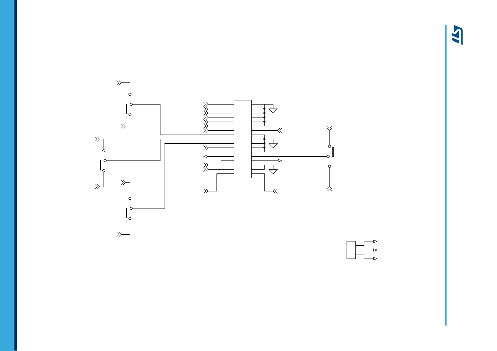
The input signals (LINx and HINx), able to drive the internal MOSFETs, are active high. A 100 kΩ (typ.) pull-down
resistor is built-in for each input signal. In order to prevent input signal oscillation, an RC filter was added on each
input and placed as close as possible to the IPM. The filter is designed using a time constant of 10 ns (1 kΩ and
10 pF).
4.2 Bootstrap capacitor
In the 3-phase inverter, the emitters of the low side MOSFETs are connected to the negative DC bus (VDC-) as
common reference ground, which allows all low side gate drivers to share the same power supply, while the
emitter of high side MOSFETs is alternately connected to the positive (VDC+) and negative (VDC-) DC bus during
running conditions.
A bootstrap method is a simple and cheap solution to supply the high voltage section. This function is normally
accomplished by a high voltage fast recovery diode. The SLLIMM 2nd series family includes a patented
integrated structure that replaces the external diode. It is realized with a high voltage DMOS functioning as diode
with series resistor. An internal charge pump provides the DMOS driving voltage. The value of the CBOOT
capacitor should be calculated according to the application condition.
This curve is taken from application note AN4768 (available on www.st.com); calculations are based on the
STGIB15CH60TS-L device, which represents the worst case scenario for this kind of calculation.
Figure Figure 9. CBOOT graph selectiongraph selection shows the behavior of CBOOT (calculated) versus
switching frequency (fsw), with different values of ΔVCBOOT for a continuous sinusoidal modulation and a duty
cycle δ = 50%.
The boot capacitor must be two or three times larger than the CBOOT calculated in the graph. For this design, a
value of 2.2 μF was selected.
Figure 9. CBOOT graph selection
4.3 Overcurrent protection
The SLLIMM 2nd series integrates a comparator for fault sensing purposes. The comparator has an internal
voltage reference VREF (510 mV typ.) connected to the inverting input, while the non-inverting input available on
the CIN pin can be connected to an external shunt resistor to implement the overcurrent protection function.
When the comparator triggers, the device enters the shutdown state.
The comparator output is connected to the SD pin in order to send the fault message to the MCU.
UM2702
Filters and key parameters
UM2702 - Rev 1 page 10/34

4.3.1 SD Pin
The SD is an input/output pin (open drain type if used as output). Taking into account the voltage reference on SD
(3.3 V), a pull up resistor of 10 kΩ (R28) is used to guarantee the right bias and consequently to keep the current
on the open drain DMOS (Iod) lower than 3 mA.
The filter on SD (R28 and C20) has to be sized to obtain the desired re-starting time after a fault event and placed
as close as possible to the SD pin.
A shutdown event can be managed by the MCU, in this case the SD functions as the input pin.
Conversely, the SD functions as an output pin when an overcurrent or undervoltage condition is detected.
4.3.2 Fault management
The SLLIMM 2nd series integrates a specific kind of fault management, useful when SD is functioning as output,
able to identify the type of fault event.
As previously described, as soon as a fault occurs, the open-drain (DMOS) is activated and LVGx outputs are
forced low.
Two types of fault can be signaled:
• Overcurrent (OC) sensed by the internal comparator (CIN);
• Undervoltage (UVLO) on supply voltage (VCC).
Each fault enables the SD open drain for a different time (see the table below).
The duration of a shutdown event therefore tells us the type of failure that has occurred.
Table 1. Fault timing
Symbol Parameter Event time SD open-drain enable time
result
OC
Overcurrent event ≤ 24 μs 24 μs
> 24 μs OC time
UVLO Undervoltage lockout event
≤ 70 μs 70 μs
> 70 μs until VCC_LS
exceeds the VCC_LS
UV turn on threshold
UVLO time
Note: typical value (TJ = -40 °C to 125 °C)
Note: without contribution of RC network on SD
Figure 10. SD failure due to overcurrent shows a shutdown as the result of an overcurrent event. During the
overcurrent, the voltage on the comparator (CIN) exceeds the threshold (0.51 V typ.) and the shutdown is able to
stop the application. In this case, the SD event time is about 24 μs (for OC event less than 24 μs).
UM2702
Overcurrent protection
UM2702 - Rev 1 page 11/34

Figure 10. SD failure due to overcurrent
Figure 11. SD failure due to undervoltage (UVLO below 70 μs) shows the shutdown event as the result of an
undervoltage condition on the VCC supply. If VCC drops below the undervoltage threshold, the shutdown can stop
the application. If the voltage on VCC rises above the VCC on threshold in less than 70 μs, the SD event time is
about 70 μs.
Figure 11. SD failure due to undervoltage (UVLO below 70 μs)
Figure 12. SD failure due to undervoltage (UVLO above 70 μs) shows the shutdown event as the result of an
undervoltage condition on the VCC supply. In this case, the drop on VCC is greater than 70 μs. The SD event time
is the same as the duration of drop.
UM2702
Overcurrent protection
UM2702 - Rev 1 page 12/34

Figure 12. SD failure due to undervoltage (UVLO above 70 μs)
4.3.3 Shunt resistor selection
The value of the shunt resistor is calculated by the following equation:
(1)
RSH=Vref
IOC
Where Vrefis the internal comparator (CIN) (0.51 V typ.) and IOC is the current of overcurrent detection level. The
maximum value of overcurrent protection level should be set less than the pulsed collector current in the
datasheet. In this design the over current threshold level is fixed @ IOC= 9.1 A.
(2)
RSH=
Vref ⋅R23 +R53
R53 +VF
IOC=
0.51 ⋅1000 + 4700
4700 + 0.18
9.1 =0.0877Ω
Where VF is the voltage drop across diodes D3, D4 and D5.
The commercial value chosen was 0.08 Ω to which corresponds a level of 9.8 A.
The power rating of the shunt resistor is calculated by the following equation:
(3)
PSH=1
2⋅Iload max
2⋅RSH ⋅ margin
Deratingratio
Where:
•Iload(max): Maximum load current of inverter
• RSH: Shunt resistor value at Tc=25°C
• Derating ratio: Power derating ratio of shunt resistor @ 100°C
• Margin: Safety margin of 30%
Iload(max) is calculated considering the RMS value of the IPM nominal current including a safety margin.
(4)
Iloadmax =Inom @80°C
2*0.85 = 4.2Arms
Power shunt value is:
(5)
PSH=1
2⋅4.22⋅0.08 ⋅1.3
0.8 =1.157W
Considering the commercial value, 2W shunt resistor was selected.
UM2702
Overcurrent protection
UM2702 - Rev 1 page 13/34

Based on the previous equations and conditions, minimum shunt resistance and power rating is summarized in
Section 4.3.3 table.
Table 2. Shunt selection
Device
OCP(peak)
[A]
Iload(max)
[Arms]
RSHUNT
[Ω]
Shunt power rating
PSH [W]
STIB1060DM2T-L 9.8 4.2 0.08 2
4.3.4 RC filter
An RC filter network is required to prevent undesired short circuit operation due to the noise on the shunt resistor.
In this design, the RC filter, composed of R23, R18, R21, R24 and C19, has a constant time of about 1.3 μs.
Adding the turn-off propagation delay of the gate driver and the MOSFET turn-off time (hundreds of nanoseconds
in total), the total delay time is less than 5 μs of short circuit withstand MOSFET time.
4.3.5 Single- or three-shunt selection
Single- or three-shunt resistor circuits can be adopted by setting the solder bridges SW5, SW6, SW7 and SW8.
The figures below illustrate how to set up the two configurations.
Figure 13. One-shunt configuration
Figure 14. Three-shunt configuration
UM2702
Overcurrent protection
UM2702 - Rev 1 page 14/34

5Current sensing amplifying network
The STEVAL-IPMM10B motor control demonstration board can be configured to run in three-shunt or single-shunt
configurations for field oriented control (FOC).
The current can be sensed thanks to the shunt resistor and amplified by using the on board operational amplifiers
or by the MCU (if equipped with op-amp).
Once the shunt configuration is chosen by setting solder bridge on SW5, SW6, SW7 and SW8 (as described in
Section 4.3.5 Single- or three-shunt selection), the user can choose to send the voltage shunt to the MCU
amplified or unamplified.
Single-shunt configuration requires a single op amp and three-shunt configuration requires three op amps;
therefore, in single-shunt configuration, the only voltage which is sent to the MCU to control the sensing is
connected to phase V through SW2.
SW1, SW2, SW4 can select which signals are sent to micro, as described below:
Table 3. Op-amp sensing configuration
Symbol Configuration Bridge Sensing
SW1
Single
Shunt
1-2
2-3
open
open
Three
Shunt
1-2
2-3
On-board op-amp
MCU op-amp
SW2
Single
Shunt
1-2
2-3
On-board op-amp
MCU op-amp
Three
Shunt
1-2
2-3
On-board op-amp
MCU op-amp
SW4
Single
Shunt
1-2
2-3
open
open
Three
Shunt
1-2
2-3
On-board op-amp
MCU op-amp
The operational amplifier TSV994 used on amplifying networks has a 20 MHz gain bandwidth and operates with a
single positive supply of 3.3 V.
The amplification network must allow bidirectional current sensing, so that an output offset VO = +1.65 V
represents zero current.
Referencing the STIB1060DM2T-L (IOCP = 9.8 A; RSHUNT = 0.08 Ω), the maximum measurable phase current,
considering that the output swings from +1.65 V to +3.3 V (MCU supply voltage) for positive currents and from
+1.65 V to 0 for negative currents is:
(6)
MaxMeasCurrent =ΔV
rm= 9.8A
(7)
rm=ΔV
MaxMeasCurrent =1.65
9.8 =0.168Ω
The overall trans-resistance of the two-port network is:
(8)
rm=RSHUNT ⋅ AMP = 0.08 ⋅ AMP = 0.168Ω
(9)
UM2702
Current sensing amplifying network
UM2702 - Rev 1 page 15/34

AMP =rm
RSHUNT =0.168
0.08 = 2.1
Finally choosing Ra=Rb and Rc=Rd, the differential gain of the circuit is:
(10)
AMP =Rc
Ra=2.1
An amplification gain of 2.1 was chosen. The same amplification is obtained for all the other devices, taking into
account the OCP current and the shunt resistance, as described in Table 1.
The RC filter for output amplification is designed to have a time constant that matches noise parameters in the
range of 1.5 μs:
(11)
4⋅ι= 4 ⋅ Re⋅ Cc= 1.5µs
(12)
Cc=1.5µs
4⋅1000 =375pF 330pFselected
Table 4. Amplifying networks
Phase
Amplifying network RC filter
RaRbRcRdReCc
Phase U R30 R32 R29 R33 R31 C25
Phase V R35 R37 R34 R39 R36 C29
Phase W R40 R42 R38 R43 R41 C31
UM2702
Current sensing amplifying network
UM2702 - Rev 1 page 16/34

6Temperature monitoring
The SLLIMM 2nd series family integrates a temperature sensor (VTSO) on the low side gate driver and an NTC
thermistor placed close to the power stage.
They can be selected via SW3.
The board is designed to use both of them to monitor the internal IPM temperature through the MCU.
6.1 Thermal sensor (VTSO)
A voltage proportional to the temperature is available on the TSO pin (17) and easily measurable on the TP20 test
pin.
To improve noise immunity, a 1 nF (C16) capacitor filter is placed on this pin.
The thermal sensor does not need any pull down resistors.
The following graph shows typical voltage variation as a function of temperature.
Figure 15. Thermal sensor voltage vs temperature
IGBT110820161234TSO
2.8
2.2
1.6
1.0
0.40 25 50 75 100
VTSO
(V)
T (°C)
Min
Max
Typ
6.2 NTC Thermistor
The embedded thermistor (85 kΩ at 25 °C) in the IPM is connected between pins T1 and T2 (26, 25).
A12 kΩ pull down resistor (R10) ensures that the voltage variation on the NTC as a function of temperature is
almost linear. This voltage is easily monitored on TP1 test pin.
The figure below shows the typical voltage on T2 as function of temperature.
UM2702
Temperature monitoring
UM2702 - Rev 1 page 17/34

Figure 16. NTC voltage vs temperature
UM2702
NTC Thermistor
UM2702 - Rev 1 page 18/34

7Firmware configuration for STM32 PMSM FOC SDK
The following table summarizes the parameters which customize the latest version of the ST FW motor control
library for permanent magnet synchronous motor (PMSM): STM32 PMSM FOC SDK for this STEVAL-IPMM10B.
Table 5. ST motor control workbench GUI parameters
Block Parameter Value
Over current protection
Comparator threshold
(13)
Vref⋅R23 + R53
R53 +VF=0.8V
Overcurrent network offset 0
Overcurrent network gain
Comparator threshold (see equation) /
Iocp (see
Section 4.3.3 Shunt resistor selection)
Bus voltage sensing Bus voltage divider 1/125
Rated bus voltage info
Min rated voltage 125 V
Max rated voltage 400 V
Nominal voltage 325 V
Current sensing
Current reading typology Single- or three-shunt
Shunt resistor value See shunt value in
Section 4.3.3 Shunt resistor selection
Amplifying network gain 2.1
Command stage
Phase U Driver HS and LS: Active high
Phase V Driver HS and LS: Active high
Phase W Driver HS and LS: Active high
UM2702
Firmware configuration for STM32 PMSM FOC SDK
UM2702 - Rev 1 page 19/34

8Connectors, jumpers and test pins
Table 6. Connectors
Connector Description/pinout
J2
Motor control connector
1 - emergency stop
3 - PWM-1H
5 - PWM-1L
7 - PWM-2H
9 - PWM-2L
11 - PWM-3H
13 - PWM-3L
15 - current phase A
17 - current phase B
19 - current phase C
21 - NTC bypass relay
23 - dissipative brake PWM
25 - +V power
27- PFC sync.
29 - PWM VREF
31 - measure phase A
33 - measure phase B
2 - GND
4 - GND
6 - GND
8 - GND
10 - GND
12 - GND
14 - HV bus voltage
16 - GND
18 - GND
20 - GND
22 - GND
24 - GND
26 - heat sink temperature
28 - VDD_m
30 - GND
32 - GND
34 - measure phase C
J3
Motor connector
•phase A
• phase B
• phase C
J4
VCC supply (20 VDC max)
•positive
• negative
J5
Hall sensors / encoder input connector
1. Hall sensors input 1 / encoder A+
2. Hall sensors input 2 / encoder B+
3. Hall sensors input 3 / encoder Z+
4. 3.3 or 5 Vdc
5. GND
J7
Supply connector (DC – 125V to 400 V)
1. + (positive terminal)
2. - (negative terminal)
Table 7. Jumpers
Jumper Description
SW3
TSO/NTC
TSO: jumper on 1-2
NTC: jumper on 2-3
UM2702
Connectors, jumpers and test pins
UM2702 - Rev 1 page 20/34
Table of contents
Other ST Motherboard manuals

ST
ST NUCLEO-WL55JC STM32WL User manual

ST
ST EVAL-FDA903U-SA User manual

ST
ST STEVAL-IHM022V1 User manual

ST
ST STEVAL-L99615C User manual

ST
ST STM3241G-EVAL User manual

ST
ST EVAL-L9001 User manual

ST
ST UM0920 User manual

ST
ST STEVAL-TSP009V2 Administrator Guide

ST
ST EVAL-L9958 User manual

ST
ST EVALCOMMBOARD User manual