List of figures
Figure 1: System architecture.....................................................................................................................5
Figure 2: STEVAL-GLA001V1 evaluation board connected to NUCLEO-F030R8 board via X-NUCLEO-
IHM09M1 expansion board.........................................................................................................................9
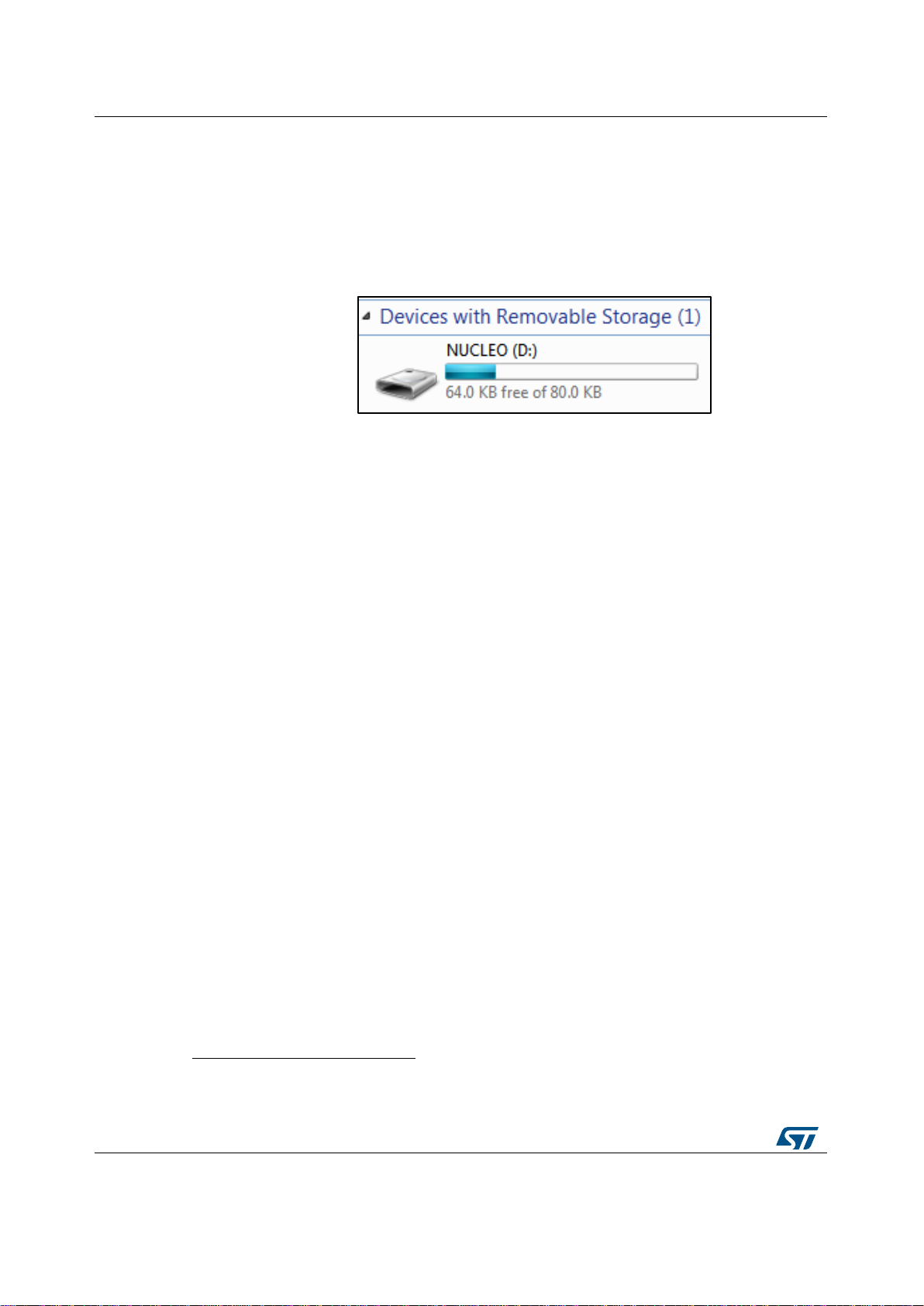
Figure 3: NUCLEO device on Windows OS .............................................................................................10
Figure 4: ST-LINK utility tool window after bin file opening......................................................................11
Figure 5: ST-LINK utility tool Target menu and Program command ........................................................11
Figure 6: ST-LINK utility tool download window .......................................................................................12
Figure 7: STSW-GLA001V1 firmware –Project workspace on IAR™ .....................................................12
Figure 8: STSW-GLA001V1 firmware –IAR workspace configuration selection.....................................13
Figure 9: STSW-GLA001V1 firmware –IAR workspace Make icon.........................................................13
Figure 10: STSW-GLA001V1 firmware –IAR workspace Download and Debug icon.............................13
Figure 11: STSW-GLA001V1 state machine............................................................................................14
Figure 12: ZVS delay principle..................................................................................................................17
Figure 13: ON/OFF control in basic/timer mode with pulse gate command timing diagram....................18
Figure 14: ON/OFF control in basic/timer mode with pulse gate command timing diagram with td_zvs >
0................................................................................................................................................................19
Figure 15: ON/OFF control in basic/timer mode with pulse gate command timing diagram with td_zvs <
0................................................................................................................................................................20
Figure 16: ON/OFF basic mode control with DC gate command timing diagram ....................................21
Figure 17: ON/OFF timer mode control with DC gate command timing diagram.....................................21
Figure 18: Phase control timing diagram..................................................................................................22
Figure 19: Phase control timing diagram with td_zvs > 0.........................................................................23
Figure 20: Phase control timing diagram with td_zvs < 0.........................................................................24
Figure 21: ZVS delay measurement - oscilloscope capture.....................................................................25
Figure 22: HyperTerminal: new connection window.................................................................................26
Figure 23: HyperTerminal: port settings ...................................................................................................26
Figure 24: Tera Term: new connection menu...........................................................................................27
Figure 25: Tera Term: setup menu...........................................................................................................28
Figure 26: Tera Term: setup menu parameters........................................................................................28
Figure 27: Tera Term: command list.........................................................................................................29
Figure 28: Tera Term: command list sample view (white background and black font) ............................29