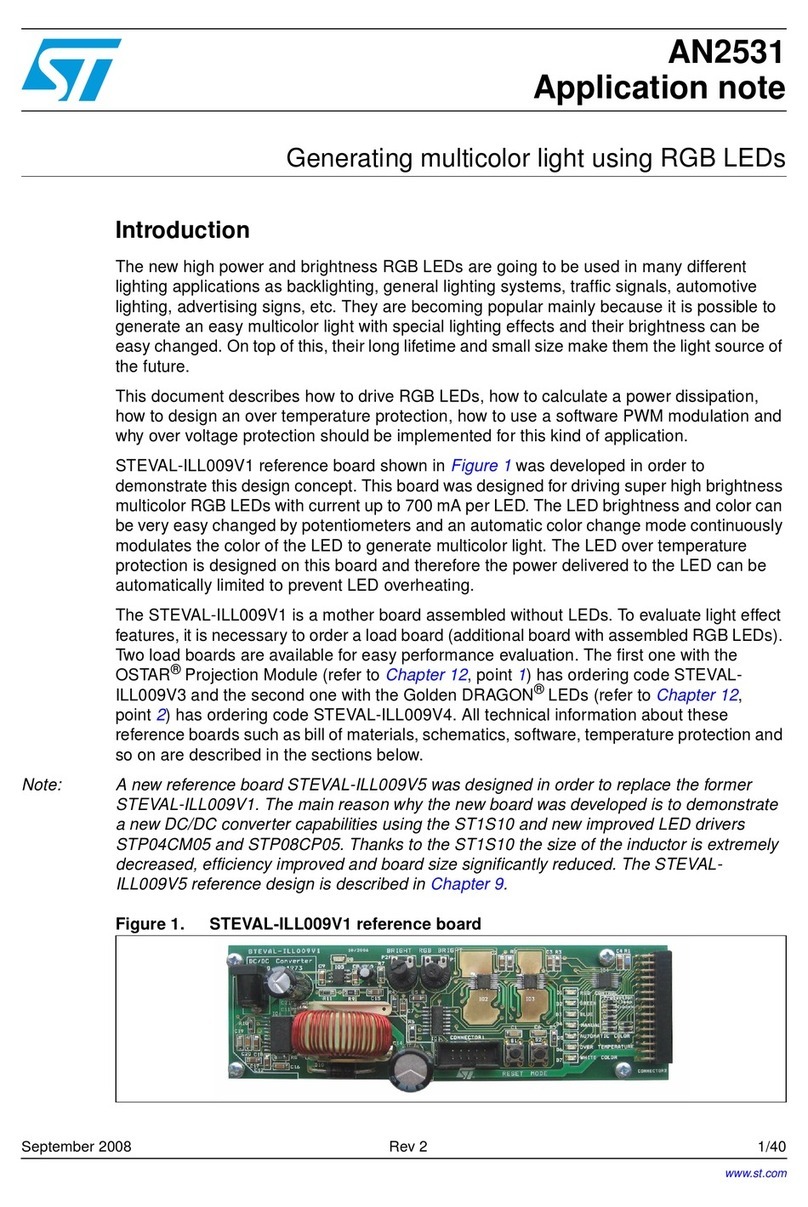
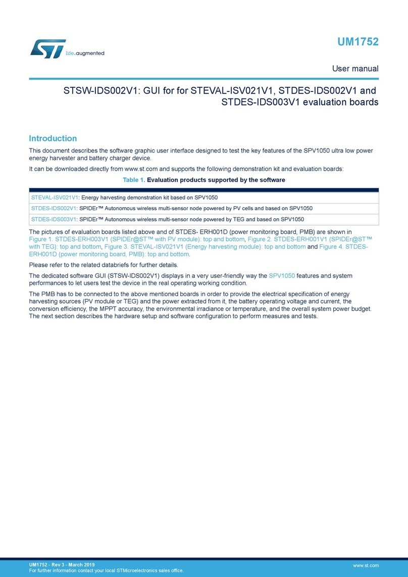
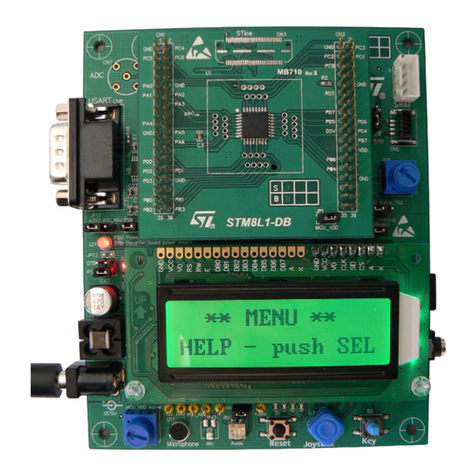
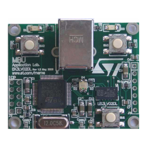
ST EVAL-L9960 User manual

June 2017 DocID030232 Rev 2 1/19
1
UM2164
User manual
EVAL-L9960/L9960T
Introduction
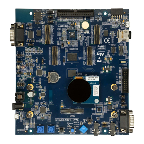
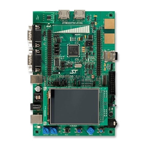
The EVAL-L9960 and EVAL-L9960T are evaluation boards designed to provide the user a
platform for the L9960 and L9960T, that are integrated H-Bridge (Twin for L9960T) for
resistive and inductive loads for automotive applications, such as throttle control actuators
or exhaust gas recirculation control valves.
The board offers all the main input/output capabilities needed to drive a DC motor properly
and to provide diagnostic functionalities.
Full diagnostic is available through SPI. By using SPI communication, it is possible to
program L9960 and L9960T while the application is running (e.i. set the current limitation).
A dedicated pin array allows connecting easily a SPC5 discovery+ board and the EVAL-
L9960/L9960T. In association with the discovery board SPC560P-DISP a dedicated SW
allows controlling a motor control application by using a PC via a USB port.
The device is an integrated H-Bridge for resistive and inductive loads for automotive
applications, such as throttle control actuators or exhaust gas recirculation control valves.
The driving strategy is enhanced by configurable PWM / DIR pins as IN1/IN2.The H-Bridge
contains integrated free-wheel diodes. In case of freewheeling conditions, the low side or
the high side transistor is switched on in parallel of its diode to reduce power dissipation.
The integrated Serial Peripheral Interface (SPI) allows device parameters adjustment and to
control all operating modes and read out diagnostic information.
Detailed failure diagnostics on each channel is provided via SPI: short circuit to battery,
short circuit to ground, short circuit overload, over temperature. Open-load can be detected
in ON condition, for the widest application ranges.
The EVAL-L9960 and EVAL-L9960T boards are suitable for both beginners and expert
users working in standalone mode connected with any control system or combined with all
SPC5 Discovery+ boards through a computer graphic interface or though embedded
application examples.
The board is compatible with both 5V and 3.3V control systems
www.st.com
Contents UM2164
2/19 DocID030232 Rev 2
Contents
1 Hardware description . . . . . . . . . . . . . . . . . . . . . . . . . . . . . . . . . . . . . . . . 5
1.1 Application Block Diagram . . . . . . . . . . . . . . . . . . . . . . . . . . . . . . . . . . . . . 5
2 EVAL-L9960 & L9960T: board description . . . . . . . . . . . . . . . . . . . . . . . 6
2.1 EVAL-L9960 & EVAL-L9960T . . . . . . . . . . . . . . . . . . . . . . . . . . . . . . . . . . 6
2.2 EVAL- L9960 / L9960T . . . . . . . . . . . . . . . . . . . . . . . . . . . . . . . . . . . . . . . . 8
2.2.1 Jumper description . . . . . . . . . . . . . . . . . . . . . . . . . . . . . . . . . . . . . . . . . 8
2.2.2 Connectors & Device . . . . . . . . . . . . . . . . . . . . . . . . . . . . . . . . . . . . . . . . 8
2.2.3 L9960T SPI configurator . . . . . . . . . . . . . . . . . . . . . . . . . . . . . . . . . . . . 10
2.3 Test Point description . . . . . . . . . . . . . . . . . . . . . . . . . . . . . . . . . . . . . . . . 10
3 Functional description . . . . . . . . . . . . . . . . . . . . . . . . . . . . . . . . . . . . . . 12
3.1 Jumper setting using L9960 & SPC5 Discovery+ board . . . . . . . . . . . . . 12
3.2 Jumper setting using L9960T & SPC5 Discovery+ board . . . . . . . . . . . . 12
4 Getting started with EVAL-L9960 & EVAL-L9960T . . . . . . . . . . . . . . . . 14
Appendix A Board layout. . . . . . . . . . . . . . . . . . . . . . . . . . . . . . . . . . . . . . . . . . . . 15
A.1 EVAL-L9960 & EVAL-L9960T PCB Layout. . . . . . . . . . . . . . . . . . . . . . . . 15
A.2 EVAL-L9960 & EVAL-L9960T schematic . . . . . . . . . . . . . . . . . . . . . . . . . 17
Revision history . . . . . . . . . . . . . . . . . . . . . . . . . . . . . . . . . . . . . . . . . . . . . . . . . . . . 18

DocID030232 Rev 2 3/19
UM2164 List of tables
3
List of tables
Table 1. Jumpers descriptions . . . . . . . . . . . . . . . . . . . . . . . . . . . . . . . . . . . . . . . . . . . . . . . . . . . . . . 8
Table 2. Connector & Device description . . . . . . . . . . . . . . . . . . . . . . . . . . . . . . . . . . . . . . . . . . . . . . 8
Table 3. Test point description . . . . . . . . . . . . . . . . . . . . . . . . . . . . . . . . . . . . . . . . . . . . . . . . . . . . . 11
Table 4. Jumpers setting using L9960 . . . . . . . . . . . . . . . . . . . . . . . . . . . . . . . . . . . . . . . . . . . . . . . 12
Table 5. Jumpers setting using L9960T . . . . . . . . . . . . . . . . . . . . . . . . . . . . . . . . . . . . . . . . . . . . . . 12
Table 6. Document revision history . . . . . . . . . . . . . . . . . . . . . . . . . . . . . . . . . . . . . . . . . . . . . . . . . 18

List of figures UM2164
4/19 DocID030232 Rev 2
List of figures
Figure 1. Application Block Diagram . . . . . . . . . . . . . . . . . . . . . . . . . . . . . . . . . . . . . . . . . . . . . . . . . . 5
Figure 2. EVAL-L9960 . . . . . . . . . . . . . . . . . . . . . . . . . . . . . . . . . . . . . . . . . . . . . . . . . . . . . . . . . . . . . 6
Figure 3. EVAL-L9960T . . . . . . . . . . . . . . . . . . . . . . . . . . . . . . . . . . . . . . . . . . . . . . . . . . . . . . . . . . . . 6
Figure 4. Gate driver board (L9907) - components and connectors - top view . . . . . . . . . . . . . . . . . . 7
Figure 5. SPC56 Discovery + Connector. . . . . . . . . . . . . . . . . . . . . . . . . . . . . . . . . . . . . . . . . . . . . . . 9
Figure 6. Motor A Connector . . . . . . . . . . . . . . . . . . . . . . . . . . . . . . . . . . . . . . . . . . . . . . . . . . . . . . . . 9
Figure 7. Motor B Connector . . . . . . . . . . . . . . . . . . . . . . . . . . . . . . . . . . . . . . . . . . . . . . . . . . . . . . . 10
Figure 8. L9960T SPI configurator . . . . . . . . . . . . . . . . . . . . . . . . . . . . . . . . . . . . . . . . . . . . . . . . . . 10
Figure 9. PCB Layout – Top view . . . . . . . . . . . . . . . . . . . . . . . . . . . . . . . . . . . . . . . . . . . . . . . . . . . 15
Figure 10. Gate driver board - PCB Layout – Bottom view . . . . . . . . . . . . . . . . . . . . . . . . . . . . . . . . . 16
Figure 11. EVAL-L9960 & EVAL-L9960T schematic . . . . . . . . . . . . . . . . . . . . . . . . . . . . . . . . . . . . . . 17

DocID030232 Rev 2 5/19
UM2164 Hardware description
17
1 Hardware description
The EVAL-L9960/L9960T is an evaluation board designed to allow the whole hardware
configuration flexibility, giving the user total access to all pins of the L9960/L9960T.
The main features are:
Total accessibility to all devices pins
Full HW compatibility with the SPC56 discovery boards through the standard SPC56
Discovery+ connector, 0.1” - 4x36 pin.
Possibility to connect generic microcontroller boards(a) by using a customised adapter.
1.1 Application Block Diagram
Figure 1. Application Block Diagram
a. A dedicated connector allows plugging the EVAL-L9960/L9960T in a SCP5 Discovery+ board easily. Further
microcontroller boards can be connected to drive the evaluation boards by using an adaptor.

EVAL-L9960 & L9960T: board description UM2164
6/19 DocID030232 Rev 2
2 EVAL-L9960 & L9960T: board description
2.1 EVAL-L9960 & EVAL-L9960T
Figure 2. EVAL-L9960
Figure 3. EVAL-L9960T

DocID030232 Rev 2 7/19
UM2164 EVAL-L9960 & L9960T: board description
17
Figure 4. Gate driver board (L9907) - components and connectors - top view

EVAL-L9960 & L9960T: board description UM2164
8/19 DocID030232 Rev 2
2.2 EVAL- L9960 / L9960T
2.2.1 Jumper description
2.2.2 Connectors & Device
Table 1. Jumpers descriptions
Name Description Type
J5 Vcc source jumper:
- 2-1= VcCC5= Vcc Micro
- 3-2= VDD5 (L7805CDT-TR)
Configurabletwopositions
jumper
J6
Vcc source jumper:
- 2-1= VDDIO= VDD5
- 2-3= VDDIO= 3,3V Micro
- 2-4= VDDIO= VDD5 (L7805CDT-TR)
- 2-5= VDDIO= 3V3 LD1117DT33CTR
Configurable three
positions jumper
J7 CSN2 Signal source jumper
1-2= CSN2=CSN1
3-2= Micro
Configurabletwopositions
jumper
J8 SDI2 Signal source jumper
- 1-2= SDI2=SDI1
- 3-2= Micro
Configurabletwopositions
jumper
J9 SCK2 Signal source jumper
- 1-2= SCK2= SCK1
- 3-2= Micro
Configurabletwopositions
jumper
J10 SDO2 Signal source jumper
- 1-2= SDO2= SDO1
- 3-2= Micro
Configurabletwopositions
jumper
J11 NDIS2 pull down resistor
- ON R=10k pull down ON/OFF jumper
J12 NDIS1 pull down resistor
- ON R=10k pull down ON/OFF jumper
J13 DIS2 pull up resistor
- ON R=10k pull up ON/OFF jumper
J14 DIS1 pull up resistor
- ON R=10k pull up ON/OFF jumper
Table 2. Connector & Device description
J1 Motor A Connector Screw
J2 Motor B Connector (Only for EVAL-L9960T) Screw
J3 VS Connector Screw

DocID030232 Rev 2 9/19
UM2164 EVAL-L9960 & L9960T: board description
17
Figure 5. SPC56 Discovery + Connector
Figure 6. Motor A Connector
J4_1,J4_2 Microcontroller connector Multipin
U1 L9960 / L9960T POWERSSO36
U2 5V Voltage Regulator L7805CDT-TR DPAK
U3 3,3 V Voltage Regulator LD1117DT33CTR DPAK
Table 2. Connector & Device description (continued)

EVAL-L9960 & L9960T: board description UM2164
10/19 DocID030232 Rev 2
Figure 7. Motor B Connector
2.2.3 L9960T SPI configurator
Figure 8. L9960T SPI configurator
2.3 Test Point description
I: Input,
O: Output

DocID030232 Rev 2 11/19
UM2164 EVAL-L9960 & L9960T: board description
17
Table 3. Test point description
TP
Name Pin Name Description I/O Type
VS VB Protected Battery supply I
VDD5 VDD5 5V Supply Input I
VCC5 VCC5 5V Supply Input Micro I
3V3 -- 3,3V Supply Input I
3V3_uC -- 3,3V Supply Input Micro I
VDDIO VDDIO VDDIO Supply Voltage I
CSN1 CSN1 SPI CSN1 Input A I
SDI1 SDI1 SPI SDI1 Input A I
SDO1 SDO1 SPI SDO1 Input A O
SCK_A SCK_A SPI Serial Clock Input A I
CSN2 CSN2 SPI CSN1 Input B I
SDI2 SDI2 SPI SDI1 Input B I
SDO2 SDO2 SPI SDO1 Input B O
SCK_B SCK_B SPI Serial Clock Input B I
DIS1 DIS1 GPIO / PWM I
NDIS1 NDIS1 GPIO / PWM I
DIS2 DIS2 GPIO / PWM I
NDIS2 NDIS2 GPIO / PWM I
IN1A IN1A GPIO / PWM I
IN2A IN2A GPIO / PWM I
IN1B IN1B GPIO / PWM I
IN2B IN2B GPIO / PWM I
GND GND Ground GND

Functional description UM2164
12/19 DocID030232 Rev 2
3 Functional description
3.1 Jumper setting using L9960 & SPC5 Discovery+ board
3.2 Jumper setting using L9960T & SPC5 Discovery+ board
Table 4. Jumpers setting using L9960
Name Description Configuration
J1 Motor A Connector Motor A
J2 Motor B Connector Not Present on EVAL-L9960
J3 VS Connector VS Connector
J4 SPC Discovery+ or other Microcontroller
Connector SPC Discovery+ or other
Microcontroller
J5 VCC Selector 3-2= VDD5 (L7805CDT-TR)
J6 VDDIO Selector 2-1= VDDIO= VDD5
OR
2-4= VDDIO= VDD5 (L7805CDT-TR)
J7 CSN2 Selector OPEN (CSN2 for L9960T)
J8 SDI2 Selector OPEN (SDI2 for L9960T)
J9 SCK2 Selector OPEN (SCK2 for L9960T)
J10 SDO2 Selector OPEN (SDO2 for L9960T)
J11 NDIS2 pull down resistor Selector OPEN (No NDIS2 pull down resistor)(1)
1. OPEN or CLOSE depending on the application
J12 NDIS1 pull down resistor Selector OPEN (No NDIS1 pull down resistor)
J13 DIS2 pull up resistor Selector OPEN (No DIS2 pull up resistor)
J14 DIS1 pull up resistor Selector OPEN (No DIS1 pull up resistor)
Table 5. Jumpers setting using L9960T
Name Description Configuration
J1 Motor A Connector Motor A
J2 Motor B Connector Motor B
J3 VS Connector VS Connector
J4 SPC Discovery+ or other Microcontroller
Connector SPC Discovery+ or other Microcontroller
J5 VCC Selector 3-2= VDD5 (L7805CDT-TR)
J6 VDDIO Selector 2-1= VDDIO= VDD5
OR
2-4= VDDIO= VDD5 (L7805CDT-TR)

DocID030232 Rev 2 13/19
UM2164 Functional description
17
J7 CSN2 Selector 1-2= CSN2=CSN1
J8 SDI2 Selector 1-2= SDI2=SDI1
J9 SCK2 Selector 1-2= SCK2=SCK1
J10 SDO2 Selector 1-2= SDO2=SDO1
J11 NDIS2 pull down resistor Selector OPEN (No NDIS2 pull down resistor)
J12 NDIS1 pull down resistor Selector OPEN (No NDIS1 pull down resistor)
J13 DIS2 pull up resistor Selector OPEN (No DIS2 pull up resistor)
J14 DIS1 pull up resistor Selector OPEN (No DIS1 pull up resistor)
Table 5. Jumpers setting using L9960T (continued)
Name Description Configuration

Getting started with EVAL-L9960 & EVAL-L9960T UM2164
14/19 DocID030232 Rev 2
4 Getting started with EVAL-L9960 & EVAL-L9960T
A dedicated Graphical User Interface (GUI) is available to set and control the EVAL-L9960 &
EVAL-L9960T board (ETC H/Bridge motor application boards for L9960) through the SPI
protocol, manage the DIS, NDIS and IN2 pins and send PWM to IN1 pins.
The GUI (STSW-L9960) has been developed using Labview® 2015 and it works with
SPC560P-DISP evaluation board programmed with a dedicated FW (GP-Pictus_v1.1.elf)
available on the ST web site.

DocID030232 Rev 2 15/19
UM2164 Board layout
17
Appendix A Board layout
A.1 EVAL-L9960 & EVAL-L9960T PCB Layout
Figure 9. PCB Layout – Top view

Board layout UM2164
16/19 DocID030232 Rev 2
Figure 10. Gate driver board - PCB Layout – Bottom view

DocID030232 Rev 2 17/19
UM2164 Board layout
17
A.2 EVAL-L9960 & EVAL-L9960T schematic
Figure 11. EVAL-L9960 & EVAL-L9960T schematic
1 2
3 4
5 6
7 8
910
11 12
13 14
15 16
17 18
19 20
21 22
23 24
25 26
27 28
29 30
31 32
33 34
35 36
37 38
39 40
41 42
43 44
45 46
47 48
49 50
51 52
53 54
55 56
57 58
59 60
61 62
63 64
66
68
65
67
X1
HE AD E R 2x34
1 2
3 4
5 6
7 8
910
11 12
13 14
15 16
17 18
19 20
21 22
23 24
25 26
27 28
29 30
31 32
33 34
35 36
37 38
39 40
41 42
43 44
45 46
47 48
49 50
51 52
53 54
55 56
57 58
59 60
61 62
63 64
66
68
65
67
X2
HEADE R 2x34
C1
C34
C2
C3
C4
C5
C6
C7
C8
C9
C10
C11
C12
C13
C14
C15
C16
C17
C18
C19
C20
C21
C22
C23
C24
C25
C26
C27
C28
C29
C30
C31
C32
C33
D2
D3
D4
D5
D6
D7
D8
D9
D1 0
D1 1
D1 2
D1 3
D1 4
D1 5
D1 6
D1 7
D1 8
D1 9
D2 0
D2 1
D2 2
D2 3
D2 4
D2 5
D2 6
D2 7
D2 8
D2 9
D3 0
D3 1
D3 2
D3 3
D1A1
A2
A3
A4
A5
A6
A7
A8
A9
A10
A11
A12
A13
A14
A15
A16
A17
A18
A19
A20
A21
A22
A23
A24
A25
A26
A27
A28
A29
A30
A31
A32
A33
A34
B1
B2
B3
B4
B5
B6
B7
B8
B9
B10
B11
B12
B13
B14
B15
B16
B17
B18
B19
B20
B21
B22
B23
B24
B25
B26
B27
B28
B29
B30
B31
B32
B33
B34 D34
PWM_H1
PWM_H2
PWM_H3
PWM_L1
PWM_L2
PWM_L3
1
2
3
J5
CON3
1
2
3
J6
CON3
1
2
3
J11
CON3
1
2
3
J12
CON3
SDO
CS
SCK
SDI
L1 47u-1A C22
10n/100V
1
2
3
J2
CON3
VIGN
SPI SDO
SPI SCK
SPI SDI
SPI CS
R1
1K -1%
R3 0
R2 0
IS1+
IS1-
R4 0
R6 0
IS2-
IS2+
C7
1uF/100V
SHS_1
GHS_1
C9
1uF/100V
GHS_2
SHS_2
C8
1uF/100V
SHS_3
GHS_3
GLS_3
GLS_1
GLS_2
SLS_1
SLS_2
SLS_3
GND
GND GND
VCC1
VCC1
GND GND
1
TP36
1
TP35
1
TP34
1
TP33
1
TP32
1
TP40
1
TP39
SDO
CS
SCK
SDI
FS_FLAG
TM
TO3
IB1
IB2
1
TP19
1
TP26
1
TP25
1
TP24
1
TP23
1
TP22
1
TP21
1
TP20
TP41 TP42 TP44
TP8
C6
100n/35V
GND
TP43
GND
1
TP9
1
TP10
1
TP11
1
TP12
1
TP13
1
TP14
1
TP15
1
TP16
1
TP17
1
TP18
1
TP27
1
TP28
1
TP29
1
TP30
1
TP31
EN1
EN2
GND GND
VCC1
VDD
INV ER T ER
C4
100n/35V
1
TP2
GND
C1
1uF/100V
1
TP1
VCAP
1TP4
1TP3
C3
100nF/100V
1
TP5
1
TP6
PGN D
1
TP7
VB
PGN D
Ignition switc h
VBatt
GND
C2
1uF/100V
INVERTER connector
J15
J16
J20
VCC
J64
1
2
3
J50
CON3
R10
3K -1%
R11
3K -1%
C30
2.2n
C29
2.2n
C28
2.2n
C18
100n
R15
4.7K
R24
4.7K
R25
4.7K
1
2
3
4
5
J65
CON5
C20
47u/16V
HALL SENSOR
HA LL1
HA LL2
HA LL3
VC C
GN D
VCC
1
2
3
4
5
J66
CON5
ENCODER
GN D
IN DE X
CHA NNE L A
VC C
CHANNEL B
VCC
D2 S2B
GND
VCC
PWM_L1
PWM_H2
PWM_L2
PWM_H3
PWM_L3
EN_I
EN_A
EN_B
EN_I
EN_A
EN_B
HALL_1 HA LL_2
HALL_3
EN1_X2 FS_FLAG
SPI CS
SPI SCK
SPI SDI SPI SDOIB1
IB2
D1
MB R B 20200
GND
GND
C10
1uF/100V
1
TP37
1TP46
1TP45
1TP47
1TP51
1TP50
1TP48
1
TP52 1
TP53
HALL_1
HALL_2
HALL_3
VCC1
J1
PGN D
GND
1
TP54
TP38
1
2
3
4
J4
CON4
C11
100nF/100V
D3
1N4007
GND
D4
LED
To board of Micro
R9
680
GND
D5
LED
VIGN
R12
1k
J17
PGN D
R14
680
D7
LED
R13
680
D6
LED
EN1 EN2
GND
VIGN2
1
TP55
1
TP56
1
TP57
GND
R16
0
PGN D GND
GLS_3 2
SL S_3 3
GLS_2 5
SL S_2 6
AGND
10
GLS_1 8
SL S_1 9
IS1+ 11
IS1- 12
IB1
14
IB2
15
SGND2
16
IS2- 17
IS2+ 18
CBS_3 20
GHS_3 21
SH S_3 22
CBS_2 24
GHS_2 25
SH S_2 26
CBS_1 28
GHS_1 29
SH S_1 30
TM
33
PWM _H1
34
PWM _H2
35
PWM _H3
36
FS_FL AG
37
CS
38
SC K
39
SI
40
SO
41
TO3
42
EN2
43 EN1
44
PWM _L 1
45
PWM _L 2
46
PWM _L 3
47
SGND1
48
Vcc 49
GCR 51
Vdd
52
DGND
53
VB 54
BST_L 56
BST_DIS
58
BST_
C60
VCAP 62
VDH 64
G
L
S
_
3
S
L
S
_
3
G
L
S
_
2
S
L
S
_
2
A
G
N
D
G
L
S
_
1
S
L
S
_
1
I
S
1
+
I
S1
-
I
B
1
I
B
2
S
G
N
D
2
I
S2
-
I
S2
+
C
B
S
_
3
G
H
S
_
3
S
H
S
_
3
C
B
S
_
2
G
H
S
_
2
S
H
S
_
2
C
B
S
_
1
G
H
S
_
1
S
H
S
_
1
T
M
P
W
M
_
H
1
P
W
M
_
H
2
PW
M
_
H
3
F
S
_
F
L
A
G
C
S
S
C
K
S
I
S
O
T
O
3
EN
2
EN
1
P
W
M
_
L
1
PW
M
_
L
2
PW
M
_
L
3
S
G
N
D
1
V
c
c
G
C
R
V
dd
D
G
N
D
V
B
B
S
T
_
L
B
S
T
_
D
I
S
B
S
T
_
C
V
C
A
P
V
D
H
PAD D OWN
65
BGND 57
U1 L9907
BST_DIS
PGN D
1
2
3
J13
CON3
BST_DIS
(Footprint "T")
12
3
4
1
2
3
4
J14
GND
VCC
IS1+
IS1-
IS2-
IS2+
SHS_3
GHS_3 GLS_3
SLS_3
GHS_2
SHS_2
GLS_2
SLS_2
SHS_1
GHS_1 GLS_1
SLS_1
IS1+
IS1-
IS2-
IS2+
PGN D
1 2
3 4
5 6
7 8
910
11 12
13 14
15 16
JP2
HEADE R 8X2
PGN D PG ND
1 2
3 4
5 6
7 8
910
11 12
13 14
15 16
JP1
HEADE R 8X2
PGN D
VCAP
VDH
Male connector (90°)
EN1_X2
R22
5,6
D12
STPS2H100A
D13
ST PS 2H 100A
D14
ST PS 2H 100A
D15
ST PS 2H 100A
D16
STPS2H100A
D17
STPS2H100A
R20
5,6
R18
5,6
R21
5,6
R19
5,6
R17
5,6
PGN D
D8
ST PS 2H 100A
D9
STPS2H100A
D10
STPS2H100A
D11
ST PS 2H 100A
GND
C5
2.2uF/100V
1
2
3
4
J34
EN2_X2
(Footprint "T")
12
3
4
EN2_X2
J25
J26
J27
J28
J30
J29
J18
J19
J21
J22
J23
J24
C21
100uF/100V
1 2
L 2 3.3uH / 2A
J7
V_ADJ
C16
100nF/100V
GND
V_ADJ
C15
100nF/16V
C14
10uF/16V
D18
1N4007
GND
GND
R8
120
R23
270
C17
10uF/16V
R26
150
12
J3
OPE N =+5V
R7
10/1W
IN
3
GND
1
OUT 4
U2 LM217M
CL O SE =+3. 3V
V_ADJ
Default = 2-3
Default= Open
Default = Cl o s e
Default = Op e n
Default= C lose
Default = Cl o s e
Default = Cl o s e
Default = 1-2
Default = Cl o s eDefault = Op e n
Default = 1-2
Default = 2-3
Default = 1-2
Default = 1-2
Default = 1-2
Default = 1-2
Default = Open
Default = Open
Default = Open
Default = Open
Default = Open
Default = Open
Default= Open
De
fault= Open
Default= Ope
n
Default= Open
Default= Open
Default= Open
J9
Default = Open
J10
Default = Open
J31
Default= Open
J32
Default= Open
C13
22uF/100V
C12
100uF/100V
PWM_H1
R5
100K
5
43
2
16
Q1 Q2
Q1
BC 846BDW1T 1G
R27
220
VIGN
GND

Revision history UM2164
18/19 DocID030232 Rev 2
Revision history
Table 6. Document revision history
Date Revision Changes
30-Jan-2017 1 Initial release.
13-Jun-2017 2 Typo.

DocID030232 Rev 2 19/19
UM2164
19
IMPORTANT NOTICE – PLEASE READ CAREFULLY
STMicroelectronics NV and its subsidiaries (“ST”) reserve the right to make changes, corrections, enhancements, modifications, and
improvements to ST products and/or to this document at any time without notice. Purchasers should obtain the latest relevant information on
ST products before placing orders. ST products are sold pursuant to ST’s terms and conditions of sale in place at the time of order
acknowledgement.
Purchasers are solely responsible for the choice, selection, and use of ST products and ST assumes no liability for application assistance or
the design of Purchasers’ products.
No license, express or implied, to any intellectual property right is granted by ST herein.
Resale of ST products with provisions different from the information set forth herein shall void any warranty granted by ST for such product.
ST and the ST logo are trademarks of ST. All other product or service names are the property of their respective owners.
Information in this document supersedes and replaces information previously supplied in any prior versions of this document.
© 2017 STMicroelectronics – All rights reserved
This manual suits for next models
1
Table of contents
Other ST Motherboard manuals

ST
ST NUCLEO-F031K6 User manual

ST
ST M24SR-DISCOVERY User manual

ST
ST STEVAL-IHM022V1 User manual

ST
ST EVALST-ISOSD61L User manual

ST
ST STFPC311 User manual

ST
ST STM32 Nucleo User manual

ST
ST STM32H757I-EVAL User manual

ST
ST STM8L1526-EVAL User manual

ST
ST SPC58XXADPT64S User manual

ST
ST AEK-MOT-TK200G1 User manual

ST
ST STM8L15LPBOARD User manual

ST
ST STEVAL-IDB007V1 User manual

ST
ST EVAL-RHRPMPOL01 User manual

ST
ST SPC58XXADPT292S User manual

ST
ST STM3220G-EVAL User manual

ST
ST STM32 Nucleo Installation and operating instructions

ST
ST EVALSPEAr320CPU User manual

ST
ST STM3210C-EVAL User manual

ST
ST STM32G4 Nucleo-64 User manual

ST
ST STM3220G-EVAL User manual