ST STEVAL-IHM022V1 User manual

September 2009 Doc ID 15451 Rev 1 1/58
UM0686
User manual
STEVAL-IHM022V1 STM32-based dual
motor FOC drive demonstration board
Introduction
The STEVAL-IHM022V1 demonstration board is designed as a dual motor field-oriented
control (FOC) development platform for STMicroelectronics’ ARM Cortex™- M3 core-based
STM32F103ZE microcontroller. The board features full speed USB 2.0 and CAN 2.0 A/B
compliant interfaces, 2 I2S channels, 2 I2C channels, 5 USART channels, 3 SPI channels, 2
DAC channels, internal 64 KB SRAM and 512 KB Flash memory, and JTAG and SWD
debugging support. The board is designed to implement multiple motor control (up to three
MC connectors are available) and offers an advanced user I/O interface (LCD QVGA display
and joystick key). Extension headers make it easy to connect a daughterboard or wrapping
board for specific applications.
The demonstration board can be ordered through order code STEVAL-IHM022V1.
Features
■Four 5 V power supply sources: 2-way screw connector, power jack, USB connector or
daughterboard
■Boot from system memory, user Flash or SRAM
■64 Mb serial Flash included
■Two RS-232 channels with RTS/CTS handshake support on one channel
■USB 2.0 full speed connection
■CAN 2.0 A/B compliant connection
■Two full featured motor control connectors for field oriented control plus PFC support on
one connector
■JTAG, SWD and trace debug support
■240 x 320 TFT color LCD
■Joystick with 4-direction control and selector
■Reset, wakeup, tamper and user button
■Extension connectors for daughterboard or wrapping board
■RoHS compliant
Figure 1. STEVAL-IHM022V1 demonstration board
AM00172V1
www.st.com
www.BDTIC.com/ST

Contents UM0686
2/58 Doc ID 15451 Rev 1
Contents
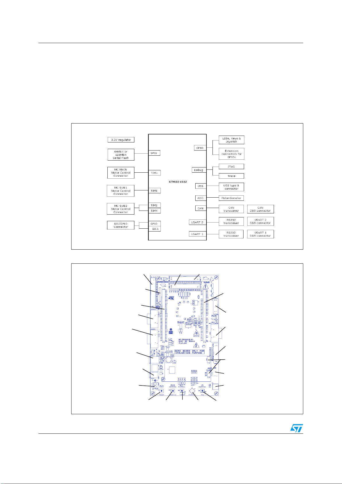
1 Hardware layout and configuration . . . . . . . . . . . . . . . . . . . . . . . . . . . . . 6
1.1 Power supply . . . . . . . . . . . . . . . . . . . . . . . . . . . . . . . . . . . . . . . . . . . . . . . 7
1.2 Boot options . . . . . . . . . . . . . . . . . . . . . . . . . . . . . . . . . . . . . . . . . . . . . . . . 7
1.3 Clock sources . . . . . . . . . . . . . . . . . . . . . . . . . . . . . . . . . . . . . . . . . . . . . . . 8
1.4 Reset sources . . . . . . . . . . . . . . . . . . . . . . . . . . . . . . . . . . . . . . . . . . . . . . 8
1.5 Serial Flash . . . . . . . . . . . . . . . . . . . . . . . . . . . . . . . . . . . . . . . . . . . . . . . . 9
1.6 CAN . . . . . . . . . . . . . . . . . . . . . . . . . . . . . . . . . . . . . . . . . . . . . . . . . . . . . . 9
1.7 RS-232 connectors . . . . . . . . . . . . . . . . . . . . . . . . . . . . . . . . . . . . . . . . . . 10
1.8 Motor control connectors . . . . . . . . . . . . . . . . . . . . . . . . . . . . . . . . . . . . . 10
1.9 USB . . . . . . . . . . . . . . . . . . . . . . . . . . . . . . . . . . . . . . . . . . . . . . . . . . . . . 13
1.10 Development and debug support . . . . . . . . . . . . . . . . . . . . . . . . . . . . . . . 14
1.11 Display and input devices . . . . . . . . . . . . . . . . . . . . . . . . . . . . . . . . . . . . . 14
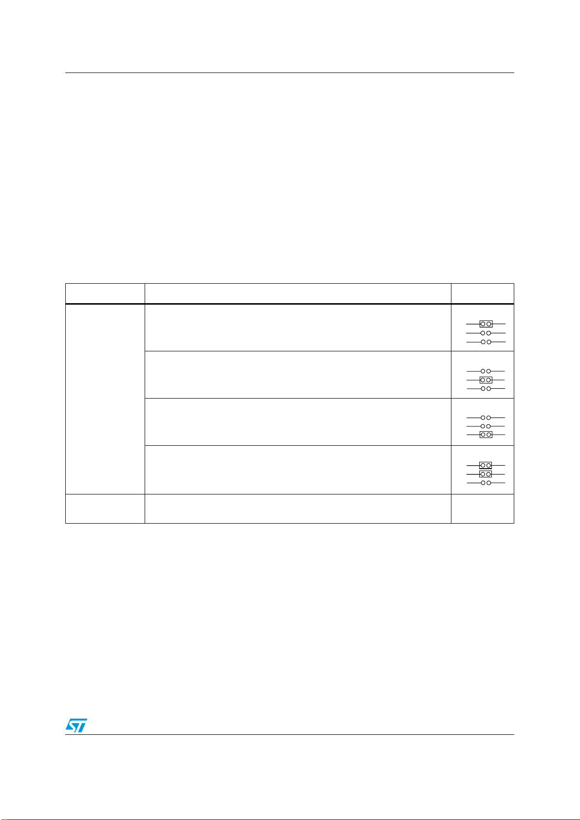
2 Connectors . . . . . . . . . . . . . . . . . . . . . . . . . . . . . . . . . . . . . . . . . . . . . . . 16
2.1 Motor control connector CON8 (MC main) . . . . . . . . . . . . . . . . . . . . . . . . 16
2.2 Motor control connector CON9 (MC sub1) . . . . . . . . . . . . . . . . . . . . . . . . 17
2.3 Motor control connector CON10 (MC sub2) . . . . . . . . . . . . . . . . . . . . . . . 19
2.4 Auxiliary motor control connector CON14 . . . . . . . . . . . . . . . . . . . . . . . . 20
2.5 CAN D-type 9-pin male connector P1 . . . . . . . . . . . . . . . . . . . . . . . . . . . 21
2.6 I2C and I/O connector CON2 . . . . . . . . . . . . . . . . . . . . . . . . . . . . . . . . . . 21
2.7 Trace debugging connector CON5 . . . . . . . . . . . . . . . . . . . . . . . . . . . . . . 22
2.8 RS-232 connector P2 with RTS/CTS handshake support . . . . . . . . . . . . 23
2.9 RS-232 connector P3 . . . . . . . . . . . . . . . . . . . . . . . . . . . . . . . . . . . . . . . . 24
2.10 JTAG debugging connector CON6 . . . . . . . . . . . . . . . . . . . . . . . . . . . . . . 24
2.11 Daughterboard extension connectors CN10 and CN11 . . . . . . . . . . . . . . 25
2.12 USB type B connector CON11 . . . . . . . . . . . . . . . . . . . . . . . . . . . . . . . . . 31
2.13 TFT LCD connector CON4 . . . . . . . . . . . . . . . . . . . . . . . . . . . . . . . . . . . . 32
2.14 Power connectors CON12 and CON13 . . . . . . . . . . . . . . . . . . . . . . . . . . 32
3 Schematic diagrams . . . . . . . . . . . . . . . . . . . . . . . . . . . . . . . . . . . . . . . . 33
4 Bill of material . . . . . . . . . . . . . . . . . . . . . . . . . . . . . . . . . . . . . . . . . . . . . 44
www.BDTIC.com/ST

List of tables UM0686
4/58 Doc ID 15451 Rev 1
List of tables
Table 1. Power supply configuration jumper settings . . . . . . . . . . . . . . . . . . . . . . . . . . . . . . . . . . . . . 7
Table 2. Boot switches . . . . . . . . . . . . . . . . . . . . . . . . . . . . . . . . . . . . . . . . . . . . . . . . . . . . . . . . . . . . 8
Table 3. Reset jumper . . . . . . . . . . . . . . . . . . . . . . . . . . . . . . . . . . . . . . . . . . . . . . . . . . . . . . . . . . . . 8
Table 4. Serial Flash-related jumpers . . . . . . . . . . . . . . . . . . . . . . . . . . . . . . . . . . . . . . . . . . . . . . . . . 9
Table 5. CAN transceiver mode selection . . . . . . . . . . . . . . . . . . . . . . . . . . . . . . . . . . . . . . . . . . . . . 9
Table 6. Motor control-related jumpers. . . . . . . . . . . . . . . . . . . . . . . . . . . . . . . . . . . . . . . . . . . . . . . 11
Table 7. Enabling the USB disconnection simulation feature . . . . . . . . . . . . . . . . . . . . . . . . . . . . . . 14
Table 8. LCD modules . . . . . . . . . . . . . . . . . . . . . . . . . . . . . . . . . . . . . . . . . . . . . . . . . . . . . . . . . . . 14
Table 9. Motor control connector CON8 pin description . . . . . . . . . . . . . . . . . . . . . . . . . . . . . . . . . . 16
Table 10. Motor control connector CON9 pin description . . . . . . . . . . . . . . . . . . . . . . . . . . . . . . . . . . 17
Table 11. Motor control connector CON10 pin description . . . . . . . . . . . . . . . . . . . . . . . . . . . . . . . . . 19
Table 12. Auxiliary motor control connector CON14 pin description . . . . . . . . . . . . . . . . . . . . . . . . . 20
Table 13. CAN D-type 9-pin male connector P1 pin description. . . . . . . . . . . . . . . . . . . . . . . . . . . . . 21
Table 14. I2C and I/O connector CON2 pin description . . . . . . . . . . . . . . . . . . . . . . . . . . . . . . . . . . . 22
Table 15. Trace debugging connector CON5 pin description . . . . . . . . . . . . . . . . . . . . . . . . . . . . . . . 22
Table 16. RS-232 connector P2 pin description . . . . . . . . . . . . . . . . . . . . . . . . . . . . . . . . . . . . . . . . . 23
Table 17. RS-232 connector P3 pin description . . . . . . . . . . . . . . . . . . . . . . . . . . . . . . . . . . . . . . . . . 24
Table 18. JTAG debugging connector CON6 pin description . . . . . . . . . . . . . . . . . . . . . . . . . . . . . . . 25
Table 19. Daughterboard extension connector CON1 . . . . . . . . . . . . . . . . . . . . . . . . . . . . . . . . . . . . 26
Table 20. Daughterboard extension connector CON3 . . . . . . . . . . . . . . . . . . . . . . . . . . . . . . . . . . . . 29
Table 21. USB type B connector CN11 pin description . . . . . . . . . . . . . . . . . . . . . . . . . . . . . . . . . . . 32
Table 22. Bill of material . . . . . . . . . . . . . . . . . . . . . . . . . . . . . . . . . . . . . . . . . . . . . . . . . . . . . . . . . . . 44
Table 23. STEVAL-IHM022V1 I/O assignment. . . . . . . . . . . . . . . . . . . . . . . . . . . . . . . . . . . . . . . . . . 52
Table 24. Document revision history . . . . . . . . . . . . . . . . . . . . . . . . . . . . . . . . . . . . . . . . . . . . . . . . . 57
www.BDTIC.com/ST

UM0686 List of figures
Doc ID 15451 Rev 1 5/58
List of figures
Figure 1. STEVAL-IHM022V1 demonstration board . . . . . . . . . . . . . . . . . . . . . . . . . . . . . . . . . . . . . . 1
Figure 2. Hardware block diagram . . . . . . . . . . . . . . . . . . . . . . . . . . . . . . . . . . . . . . . . . . . . . . . . . . . . 6
Figure 3. STEVAL-IHM022V1 demonstration board layout . . . . . . . . . . . . . . . . . . . . . . . . . . . . . . . . . 6
Figure 4. Motor control connector CON8 (top view) . . . . . . . . . . . . . . . . . . . . . . . . . . . . . . . . . . . . . 16
Figure 5. Motor control connector CON9 (top view) . . . . . . . . . . . . . . . . . . . . . . . . . . . . . . . . . . . . . 17
Figure 6. Motor control connector CON10 (top view) . . . . . . . . . . . . . . . . . . . . . . . . . . . . . . . . . . . . 19
Figure 7. Auxiliary motor control connector CON14 (top view) . . . . . . . . . . . . . . . . . . . . . . . . . . . . . 20
Figure 8. CAN D-type 9-pin male connector P1 (front view) . . . . . . . . . . . . . . . . . . . . . . . . . . . . . . . 21
Figure 9. I2C and I/O connector CON2 (top view) . . . . . . . . . . . . . . . . . . . . . . . . . . . . . . . . . . . . . . . 21
Figure 10. Trace debugging connector CON5 (top view) . . . . . . . . . . . . . . . . . . . . . . . . . . . . . . . . . . 22
Figure 11. RS-232 connector P2 with RTS/CTS handshake support (front view) . . . . . . . . . . . . . . . . 23
Figure 12. RS-232 connector P3 (front view). . . . . . . . . . . . . . . . . . . . . . . . . . . . . . . . . . . . . . . . . . . . 24
Figure 13. JTAG debugging connector CON6 (top view) . . . . . . . . . . . . . . . . . . . . . . . . . . . . . . . . . . 24
Figure 14. USB type B connector CN11 (front view) . . . . . . . . . . . . . . . . . . . . . . . . . . . . . . . . . . . . . . 31
Figure 15. Power supply connector CON12 (front view) . . . . . . . . . . . . . . . . . . . . . . . . . . . . . . . . . . . 32
Figure 16. STM32F103ZE MCU . . . . . . . . . . . . . . . . . . . . . . . . . . . . . . . . . . . . . . . . . . . . . . . . . . . . . 34
Figure 17. Extension and I2C I/O connectors . . . . . . . . . . . . . . . . . . . . . . . . . . . . . . . . . . . . . . . . . . . 35
Figure 18. Joystick, buttons and LCD connections . . . . . . . . . . . . . . . . . . . . . . . . . . . . . . . . . . . . . . . 36
Figure 19. JTAG and trace connectors . . . . . . . . . . . . . . . . . . . . . . . . . . . . . . . . . . . . . . . . . . . . . . . . 37
Figure 20. Motor control connector main . . . . . . . . . . . . . . . . . . . . . . . . . . . . . . . . . . . . . . . . . . . . . . . 38
Figure 21. Motor control connector sub1 . . . . . . . . . . . . . . . . . . . . . . . . . . . . . . . . . . . . . . . . . . . . . . . 39
Figure 22. Motor control connector sub2 . . . . . . . . . . . . . . . . . . . . . . . . . . . . . . . . . . . . . . . . . . . . . . . 40
Figure 23. Peripherals . . . . . . . . . . . . . . . . . . . . . . . . . . . . . . . . . . . . . . . . . . . . . . . . . . . . . . . . . . . . . 41
Figure 24. Power supply . . . . . . . . . . . . . . . . . . . . . . . . . . . . . . . . . . . . . . . . . . . . . . . . . . . . . . . . . . . 42
Figure 25. RS-232 connectors . . . . . . . . . . . . . . . . . . . . . . . . . . . . . . . . . . . . . . . . . . . . . . . . . . . . . . . 43
www.BDTIC.com/ST

Hardware layout and configuration UM0686
6/58 Doc ID 15451 Rev 1
1 Hardware layout and configuration
The STEVAL-IHM022V1 demonstration board is designed around the STM32F103ZE in
144-pin TQFP package. The hardware block diagram in Figure 2 illustrates the connection
between the STM32F103ZE peripherals and connectors/devices on the board (LCD, SPI
Flash, USART, USB, CAN bus, I2C bus and motor control). The board layout diagram in
Figure 3 shows the location of the features on the demonstration board.
Figure 2. Hardware block diagram
Figure 3. STEVAL-IHM022V1 demonstration board layout
AM03527v1
AM03528v1
CON8
Motor Control Main
CON10
Motor Control Sub2
CON14
Motor Control
Sub2 Aux
CON3
Extension Connector
P3
USART1
CON11
USB
CON12
+5V power
CON13
+5V power
S1
Reset
SW2
Wake-up
SW1
Tamper
U1
Joystick
SW3
Key
RV1
Potentiometer
CON5
Trace
CON6
JTAG
P1
CAN
CON2
I2C/IOS
CON1
Extension
Connector
CON4
Color LCD connector
P2
USART2
www.BDTIC.com/ST

UM0686 Hardware layout and configuration
Doc ID 15451 Rev 1 7/58
1.1 Power supply
The STEVAL-IHM022V1 demonstration board is designed to be powered by a 5 V DC power
supply and to be protected from incorrect power plug-in events by a PolyZen U5. The
demonstration board can be configured to use any of following three power sources:
●5 V DC power adapter connected to power jack CON12 (DC5V on the silk screen).
Alternatively, 5 V DC can be provided through 2-way screw connector CON13 (aux
DC5V on the silk screen) when using a generic DC power supply
●5 V DC power with 500 mA limit from the type-B USB connector CON11 (USB B on the
silkscreen)
●5 V DC power from daughterboard extension connectors CON1 and CON3
The power supply is configured by setting jumpers JP9, JP10, JP11 and JP12 as described
in Ta b l e 1 .
The D5 LED is lit when the demonstration board is powered correctly.
1.2 Boot options
The STEVAL-IHM022V1 demonstration board can be booted from:
●embedded user Flash
●embedded SRAM for debugging
●system memory with boot loader for ISP
The boot option is configured by setting switch BOOT0 and BOOT1 as described in Ta bl e 2 .
Table 1. Power supply configuration jumper settings
Jumper Power supply option Setting
JP9,JP10,JP11
For power supply from power jack CON12 or 2-way screw connector CON13,
place a jumper on JP9 only (default setting).
For power supply from the daughterboard extension connectors CON1 and
CON3, place a jumper on JP10 only.
For power supply from USB connector CON11, place a jumper on JP11 only.
For power supply from power supply jack CON12 to both the STEVAL-
IHM022V1 and the daughterboard connected on CON1 and CON3, place
jumpers on JP9 and JP10 as shown (the daughterboard must not have its own
power supply connected).
JP12 Enables consumption measurement of both VDD and VDDA.
Default setting: fitted
JP9
JP10
JP11
JP9
JP10
JP11
JP9
JP10
JP11
JP9
JP10
JP11
www.BDTIC.com/ST

Hardware layout and configuration UM0686
8/58 Doc ID 15451 Rev 1
1.3 Clock sources
The two clock sources available on the STEVAL-IHM022V1 demonstration board for the
STM32F103ZE and RTC are:
●Y1 - 32 kHz crystal for embedded RTC
●Y2 - 8 MHz crystal for STM32F103ZE microcontroller
1.4 Reset sources
The demonstration board reset signal is active low, and the reset sources include:
●reset button S1
●debugging tools from JTAG connector CON6 and trace connector CON5
●daughterboard from CON1
Table 2. Boot switches
Switch Boot option Switch
configuration
BOOT0
BOOT1
User Flash: set the BOOT0 switch as shown. BOOT1 is not required for this
configuration (default setting).
Embedded SRAM: set the BOOT0 and BOOT1 switches as shown.
System memory: set the BOOT0 and BOOT1 switches as shown.
Table 3. Reset jumper
Jumper Description
JP3
Enable the reset of the STM32F103ZE embedded JTAG TAP controller each time a
system reset occurs. JP3 connects the TRST signal from the JTAG connection with
the system reset signal RESET#.
Default setting: no jumper placed
www.BDTIC.com/ST

UM0686 Hardware layout and configuration
Doc ID 15451 Rev 1 9/58
1.5 Serial Flash
A 64 (or 128) Mbit serial Flash is connected to SPI1 of the STM32F103ZE. SPI1 pins NSS,
MISO, MOSI and SCK are multiplexed with other peripherals, such as motor control timers
and JTAG debug. Ta bl e 4 lists the jumper configurations for enabling SPI1 peripheral
communication with serial Flash.
1.6 CAN
The STEVAL-IHM022V1 demonstration board supports CAN 2.0 A/B-compliant CAN bus
communication based on a 3.3 V CAN transceiver. High-speed mode, standby mode and
slope control mode are available and can be selected through JMP2.
Table 4. Serial Flash-related jumpers
Jumper Description
JP14 Serial Flash chip select is managed by I/O pin PA15. The jumper must be
positioned on JP14 as shown.
JP15 Serial Flash chip clock is managed by I/O pin PB3. The jumper must be
positioned on JP15 as shown.
JP16 Serial Flash chip MISO is managed by I/O pin PB4. The jumper must be
positioned on JP16 as shown.
JP14
1
2
3
4
JP15
1
2
3
4
JP16
1
2
3
4
Table 5. CAN transceiver mode selection
Jumper Description
JMP2
Standby mode: Place the jumper on pins 2—1 of JMP2, as shown.
High-speed mode: Place the jumper on pins 3—2 of JMP2, as shown
(default setting).
Slope control mode: JMP2 is open (no jumper added).
JP8 CAN terminal resistor is enabled when JP8 is fitted
Default setting: not fitted
JMP2
3 2
1
JMP2
3 2
1
JMP2
3 2
1
www.BDTIC.com/ST

Hardware layout and configuration UM0686
10/58 Doc ID 15451 Rev 1
1.7 RS-232 connectors
Two D-type 9-pin connectors P3 (USART1) and P2 (USART2) are available on the STEVAL-
IHM022V1 demonstration board. The USART1 connector is connected to RS-232
transceiver U10, while the USART2 connector with RTS/CTS handshake signal support is
connected to RS-232 transceiver U9.
1.8 Motor control connectors
The STEVAL-IHM022V1 demonstration board supports control of up to three 3-phase
brushless motors via three 34-pin connectors: CON8 (MC main), CON9 (MC sub1) and
CON10 (MC sub2). Each connector provides all required control and feedback signals to
and from the motor power-driving board. Available signals which are common to all these
connectors include:
– emergency stop
– motor speed
– 3-phase motor current
– bus voltage sense
– heatsink temperature sense from the motor driving board
– 6 channels of PWM control signals to the motor driving circuit.
For third-motor control connector MC sub2, the 6 PWM channels can be derived either by
using two general-purpose timers working in tandem, or by using just one GP timer plus
additional external circuitry for complementary PWM signals. An auxiliary connector (MC
sub2 Aux) is available on the demonstration board to connect a daughterboard for additional
logic.
The MC main connector features additional sensing signals (AC bus, DC bus and input
current) for PFC (power factor control) controller management.
The I/O pins used on the motor control connectors are multiplexed with some peripherals on
the board. Either motor control connectors or multiplexed peripherals can be enabled by
setting the jumpers, as described inTable 6: Motor control-related jumpers.
www.BDTIC.com/ST

UM0686 Hardware layout and configuration
Doc ID 15451 Rev 1 11/58
Table 6. Motor control-related jumpers
Jumper Description Multiplexed peripheral
JMP3
MC sub2 EncA is enabled when JMP3 is configured as shown:
MC main EncA is enabled when JMP3 is configured as shown:
JMP4
MC sub2 EncB is enabled when JMP4 is configured as shown:
MC main EncB is enabled when JMP4 is configured as shown.
JMP5
MC sub2 EncIndex is enabled when JMP5 is configured as
shown:
MC main EncIndex is enabled when JMP5 is configured as
shown:
JMP6
MC sub2 Heatsink Temp is enabled when JMP6 is configured
as shown:
MC main PFC Iac is enabled when JMP6 is configured as
shown:
JMP7
Potentiometer reading is enabled when JMP7 is configured as
shown:
MC sub2 Bus Voltage is enabled when JMP7 is configured as
shown:
ADC3_IN7
JMP3
1
2
3
JMP3
1
2
3
JMP4
1
2
3
JMP4
1
2
3
JMP5
1
2
3
JMP5
1
2
3
JMP6
1
2
3
JMP6
1
2
3
JMP7
1
2
3
JMP7
1
2
3
www.BDTIC.com/ST

Hardware layout and configuration UM0686
12/58 Doc ID 15451 Rev 1
JMP8
MC sub2 PWM WL is enabled when JMP8 is configured as
shown:
MC sub1 EncIndex is enabled when JMP8 is configured as
shown:
JMP9
MC sub2 PWM VL is enabled when JMP9 is configured as
shown:
MC sub1 EncB is enabled when JMP9 is configured as shown:
JMP10
MC sub2 PWM UL is enabled when JMP10 is configured as
shown:
MC sub1 EncA is enabled when JMP10 is configured as shown:
JP13 MC main PFC Vac is enabled when JP13 is configured as
shown:
DAC
JP14 MC sub2 emergency stop is enabled when JP14 is configured
as shown:
JTAG, SPI1
JP15 MC sub2 PWM URef is enabled when JP15 is configured as
shown:
JTAG, SPI1
JP16,
JP5
MC main PFC Sync1 is enabled when JP16 is configured as
shown. JTAG debugging is disabled when JP16 is fitted
between the 2—4 pins.
JP5 fitted allows a PFC synchronization signal to be redirected
to the timer 3 input capture 1 pin, in addition to the timer 3
external trigger input.
Default setting: fitted
JTAG, SPI1
Table 6. Motor control-related jumpers (continued)
Jumper Description Multiplexed peripheral
JMP8
1
2
3
JMP8
1
2
3
JMP9
1
2
3
JMP9
1
2
3
JMP10
1
2
3
JMP10
1
2
3
JP13
JP14
1
2
3
4
JP15
1
2
3
4
JP16
1
2
3
4
JP5
www.BDTIC.com/ST

UM0686 Hardware layout and configuration
Doc ID 15451 Rev 1 13/58
1.9 USB
The STEVAL-IHM022V1 demonstration board supports USB 2.0-compliant full-speed
communication via a USB type B connector (CON11). The board can be powered by this
USB connection at 5 V DC with a 500 mA current limit. USB disconnection simulation can
be implemented by disconnecting the 1.5 k pull-up resistor from the USB+ line. The USB
disconnection simulation feature is enabled by setting JMP1.
JP4
A jumper on JP4 should be fitted to enable filtering when an
analog signal is present on pin 31 of CON8 (e.g. a signal
generated by a tachometer). It should be not fitted if a signal
from an encoder is used.
Default setting: not fitted
JP6
A jumper on JP6 should be fitted to enable filtering when an
analog signal is present on pin 31 of CON9 (e.g. a signal
generated by a tachometer). It should be not fitted if a signal
from an encoder is used.
Default setting: not fitted
JP7
A jumper on JP7 should be fitted to enable filtering when an
analog signal is present on pin 31 of CON10 (e.g. a signal
generated by a tachometer). It should be not fitted if a signal
from an encoder is used.
Default setting: not fitted
J1
J1 swaps timer 8 channel 3 PWM outputs between pin 11 (MC
WH) and pin 13 (MC WL) of MC sub1 connector.
Default setting: as shown.
J2
J2 swaps MC sub1 bus voltage and MC sub1 currentB analog
signals between pin 44 (ADC12_IN14) and pin 20 (ADC3_IN6)
of the STM32 MCU.
Default setting: as shown.
Table 6. Motor control-related jumpers (continued)
Jumper Description Multiplexed peripheral
1
6
J1
3 4
2
5
21
4
6
J2
3
5
www.BDTIC.com/ST

Hardware layout and configuration UM0686
14/58 Doc ID 15451 Rev 1
1.10 Development and debug support
The two debug connectors available on the STEVAL-IHM022V1 demonstration board are:
●CON6 - a standard 20-pin JTAG interface connector that is compliant with ARM7 and
ARM9 debug tools.
●CON5 - a SAMTEC 20-pin connector (code FTR-110-01-S-D) for both SWD and trace
that is compliant with ARM CoreSight debug tools.
1.11 Display and input devices
The 240 x 320 TFT color LCD and 4 general-purpose LEDs (D1, D3, D3, D4) are available
as display devices. A 4-direction joystick with selection key (U1), a general-purpose button
(SW3), a wakeup button (SW2) and a tamper detection button (SW1) are available as input
devices.
Jumper JMP3 should be kept open to enable wakeup button SW2, which shares the same
I/O with motor control connectors MC main and MC sub2.
Table 7. Enabling the USB disconnection simulation feature
Jumper Description
JMP1
The USB 1.5 k pull-up resistor is always connected to the USB+ line when
JMP1 is set as shown (default setting):
The USB 1.5 k pull-up resistor can be disconnected by software from the
USB+ line when JMP1 is set as shown. In this case, the USB
connect/disconnect features are managed by standard IO port PD8.
JMP1
1 2
3
JMP1
1 2
3
Table 8. LCD modules
TFT LCD CON4
Pin on CON4 Description Pin connection
1CSPB2
2 SCL PB13
3 SDI PB15
4RSPD7
5WRPD15
6RDGND
7 SDO PB14
8 RESET# NRST
9 VDD +3.3 V
www.BDTIC.com/ST

UM0686 Hardware layout and configuration
Doc ID 15451 Rev 1 15/58
10 VCI +3.3 V
11 GND GND
12 GND GND
13 BL VDD +3.3 V
14 BL control PA8
15 BL GND GND
16 BL GND GND
Table 8. LCD modules (continued)
TFT LCD CON4
Pin on CON4 Description Pin connection
www.BDTIC.com/ST

Connectors UM0686
16/58 Doc ID 15451 Rev 1
2 Connectors
2.1 Motor control connector CON8 (MC main)
Figure 4. Motor control connector CON8 (top view)
Table 9. Motor control connector CON8 pin description
CON8 pin number Description Pin of STM32F103ZE
1 Emergency stop PE15
2 PFC OCP sense PE1
3 PWM-UH PE9
4GND
5 PWM-UL PE8
6GND
7 PWM-VH PE11
8GND
9 PWM-VL PE10
10 GND
11 PWM-WH PE13
12 GND
13 PWM-WL PE12
14 Bus voltage PA3
15 Phase A current PC1
16 GND
17 Phase B current PC2
18 GND
19 Phase C current PC3
20 GND
21 NTC bypass relay PD10
22 PFC Vac sense PA5
AM03529v1
13579111315171921232527293133
2468101214161820222426283034
www.BDTIC.com/ST

UM0686 Connectors
Doc ID 15451 Rev 1 17/58
2.2 Motor control connector CON9 (MC sub1)
Figure 5. Motor control connector CON9 (top view)
23 Dissipative brake PWM PB8
24 PFC Iac sense PA4
25 +5 V power +5 V
26 Heatsink temperature PF6
27 PFC SYNC PB4 and PD2
28 3.3 V power +3.3 V
29 PFC PWM PC9
30 GND
31 Encoder A PA0
32 GND
33 Encoder B PA1
34 Encoder index PA2
Table 9. Motor control connector CON8 pin description (continued)
CON8 pin number Description Pin of STM32F103ZE
Table 10. Motor control connector CON9 pin description
CON9 pin number Description Pin of STM32F103ZE
1 Emergency stop PA6
2GND
3 PWM-UH PC6
4GND
5PWM-ULPA7
6GND
7 PWM-VH PC7
8GND
9 PWM-VL PB0
AM03530v1
13579111315171921232527293133
2468101214161820222426283034
www.BDTIC.com/ST

Connectors UM0686
18/58 Doc ID 15451 Rev 1
10 GND
11 PWM-WH PB1 / PC8 (1)
12 GND
13 PWM-WL PC8 / PB1 (1)
14 Bus voltage PC4 / PF8(2)
15 Phase A current PC0
16 GND
17 Phase B current PF8 / PC4 (2)
18 GND
19 Phase C current PC5
20 GND
21 NTC bypass relay PD11
22 GND
23 Dissipative brake PWM PB9
24 GND
25 +5 V power +5 V
26 Heatsink temperature PF7
27 PFC SYNC N.C.
28 3.3 V power +3.3 V
29 PFC PWM N.C.
30 GND
31 Encoder A PD12
32 GND
33 Encoder B PD13
34 Encoder index PD14
1. Depends on J1 connector jumper position (see Section 1.8)
2. Depends on J2 connector jumper position (see Section 1.8)
Table 10. Motor control connector CON9 pin description (continued)
CON9 pin number Description Pin of STM32F103ZE
www.BDTIC.com/ST

UM0686 Connectors
Doc ID 15451 Rev 1 19/58
2.3 Motor control connector CON10 (MC sub2)
Figure 6. Motor control connector CON10 (top view)
Table 11. Motor control connector CON10 pin description
CON10 pin number Description Pin of STM32F103ZE
1 Emergency stop PA15
2GND
3 PWM-UH PB3
4GND
5PWM-ULPD12
6GND
7 PWM-VH PB10
8GND
9PWM-VLPD13
10 GND
11 PWM-WH PB11
12 GND
13 PWM-WL PD14
14 Bus voltage PF9
15 Phase A current PF10
16 GND
17 Phase B current N.C.
18 GND
19 Phase C current N.C.
20 GND
21 NTC bypass relay PD9
22 GND
23 Dissipative brake PWM PE7
24 GND
AM03531v1
13579111315171921232527293133
2468101214161820222426283034
www.BDTIC.com/ST

Connectors UM0686
20/58 Doc ID 15451 Rev 1
2.4 Auxiliary motor control connector CON14
For a third-motor operations, there is no dedicated advanced timer peripheral. In this case,
the 6 PWM signals needed to drive a 3PH power stage can be derived either by using two
GP timers (TIM2 and TIM4 working in tandem), or a single GP timer plus additional external
circuitry, plugged into the CON14 connector, to generate the remaining 3 complementary
PWM signals.
Figure 7. Auxiliary motor control connector CON14 (top view)
25 +5 V power +5V
26 Heatsink temperature PA4
27 PFC SYNC N.C.
28 3.3 V power +3.3 V
29 PFC PWM N.C.
30 GND
31 Encoder A PA0
32 GND
33 Encoder B PA1
34 Encoder index PA2
Table 11. Motor control connector CON10 pin description (continued)
CON10 pin number Description Pin of STM32F103ZE
Table 12. Auxiliary motor control connector CON14 pin description
CON14 pin number Description
1 MC sub2 PWM UH
2 MC sub2 PWM URef
3 MC sub2 PWM VH
4 MC sub2 PWM VRef
5 MC sub2 PWM WH
6MCsub2PWMWRef
7 MC sub2 PWM UL
AM03532v1
123456789
www.BDTIC.com/ST
Other manuals for STEVAL-IHM022V1
2
Table of contents
Other ST Motherboard manuals

ST
ST STM32439I-EVAL User manual

ST
ST EVALSTGAP2S User manual

ST
ST STEVAL-IDB007V Series User manual

ST
ST STM32U5 User manual

ST
ST STEVAL-IHM011V1 User manual

ST
ST STM3210C-EVAL User manual

ST
ST NUCLEO-F207ZG User manual

ST
ST STM3241G-EVAL User manual

ST
ST STEVAL-SP1ML915 User manual

ST
ST STEVAL-WESU1 User manual

ST
ST EVSPIN32G4-DUAL User manual

ST
ST STM3221G-EVAL User manual

ST
ST STM32373C-EVAL User manual

ST
ST STM32H753I-EVAL User manual

ST
ST AN3959 Installation and operating instructions

ST
ST STEVAL-L99615C User manual

ST
ST EVAL-L9001 User manual

ST
ST STM3210E-EVAL User manual

ST
ST STEVAL-AKI002V1 User manual

ST
ST UM0527 User manual