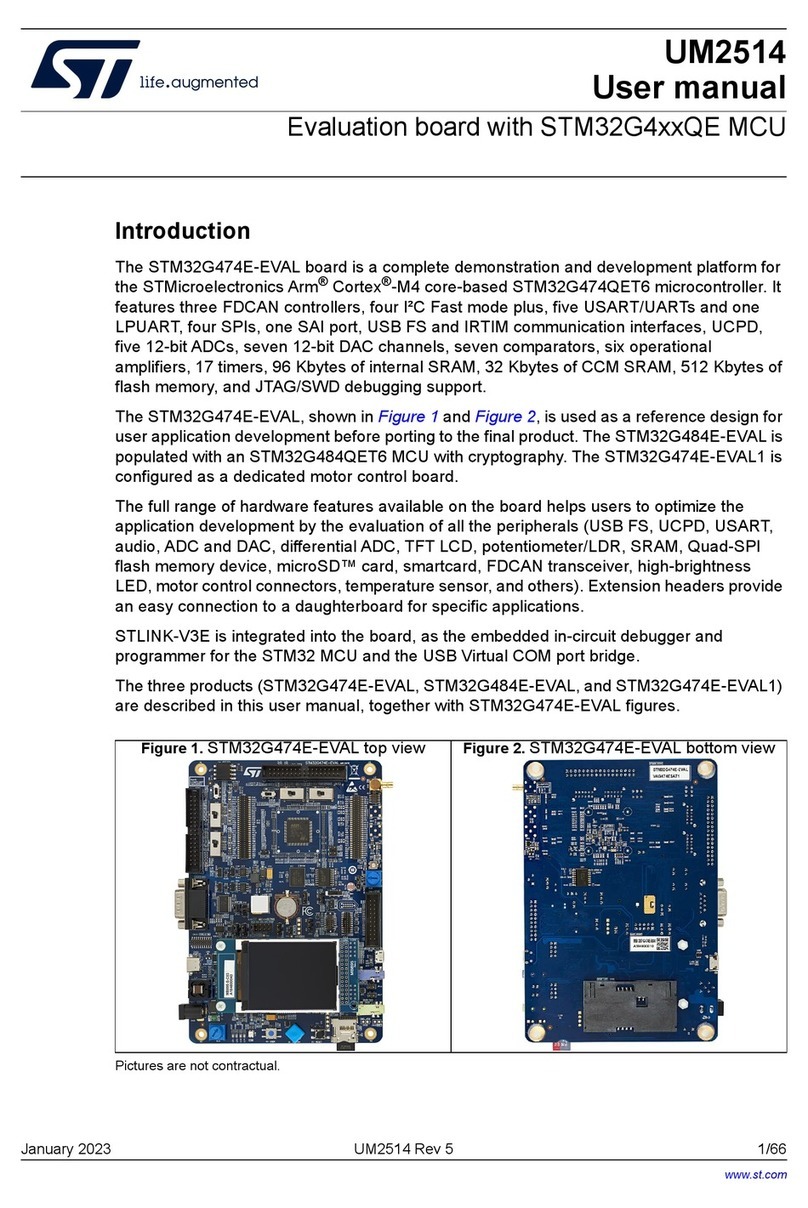
ST STM3210E-EVAL User manual

November 2008 Rev 3 1/48
UM0488
User manual
STM3210E-EVAL
evaluation board
Introduction
The STM3210E-EVAL evaluation board is designed as a complete development platform for
STMicroelectronic's ARM Cortex-M3 core-based STM32F103Z microcontroller with full
speed USB2.0, CAN2.0A/B compliant interface, two I2S channels, two I2C channels, five
USART channels with smartcard support, three SPI channels, two DAC channels, FSMC
interface, SDIO, internal 64 KB SRAM and 512 KB Flash, JTAG and SWD debug support.
The full range of hardware features on the board helps you to evaluate all peripherals (USB,
motor control, CAN, MicroSD card, smartcard, USART, NOR Flash, NAND flash, SRAM)
and develop your own applications. Extension headers make it possible to easily connect a
daughter board or wrapping board for your specific application.
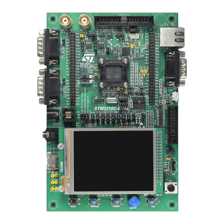
Figure 1. STM3210E-EVAL evaluation board
Order code
To order the STM32F103Z evaluation board, use the order code STM3210E-EVAL.
www.st.com

Contents UM0488
2/48
Contents
1 Overview . . . . . . . . . . . . . . . . . . . . . . . . . . . . . . . . . . . . . . . . . . . . . . . . . . 3
1.1 Features . . . . . . . . . . . . . . . . . . . . . . . . . . . . . . . . . . . . . . . . . . . . . . . . . . . 3
1.2 Demonstration software . . . . . . . . . . . . . . . . . . . . . . . . . . . . . . . . . . . . . . . 3
2 Hardware layout and configuration . . . . . . . . . . . . . . . . . . . . . . . . . . . . . 4
2.1 Power supply . . . . . . . . . . . . . . . . . . . . . . . . . . . . . . . . . . . . . . . . . . . . . . . 6
2.2 Boot option . . . . . . . . . . . . . . . . . . . . . . . . . . . . . . . . . . . . . . . . . . . . . . . . . 7
2.3 Clock source . . . . . . . . . . . . . . . . . . . . . . . . . . . . . . . . . . . . . . . . . . . . . . . . 7
2.4 Reset source . . . . . . . . . . . . . . . . . . . . . . . . . . . . . . . . . . . . . . . . . . . . . . . 7
2.5 Audio . . . . . . . . . . . . . . . . . . . . . . . . . . . . . . . . . . . . . . . . . . . . . . . . . . . . . 8
2.6 Serial Flash . . . . . . . . . . . . . . . . . . . . . . . . . . . . . . . . . . . . . . . . . . . . . . . . 8
2.7 CAN . . . . . . . . . . . . . . . . . . . . . . . . . . . . . . . . . . . . . . . . . . . . . . . . . . . . . . 8
2.8 RS232 connectors . . . . . . . . . . . . . . . . . . . . . . . . . . . . . . . . . . . . . . . . . . . 9
2.9 Motor control . . . . . . . . . . . . . . . . . . . . . . . . . . . . . . . . . . . . . . . . . . . . . . . 9
2.10 Smartcard . . . . . . . . . . . . . . . . . . . . . . . . . . . . . . . . . . . . . . . . . . . . . . . . . 10
2.11 MicroSD card . . . . . . . . . . . . . . . . . . . . . . . . . . . . . . . . . . . . . . . . . . . . . . 10
2.12 Temperature sensor . . . . . . . . . . . . . . . . . . . . . . . . . . . . . . . . . . . . . . . . . 11
2.13 Analog input . . . . . . . . . . . . . . . . . . . . . . . . . . . . . . . . . . . . . . . . . . . . . . . 11
2.14 IrDA . . . . . . . . . . . . . . . . . . . . . . . . . . . . . . . . . . . . . . . . . . . . . . . . . . . . . 11
2.15 USB . . . . . . . . . . . . . . . . . . . . . . . . . . . . . . . . . . . . . . . . . . . . . . . . . . . . . 11
2.16 Development and debug support . . . . . . . . . . . . . . . . . . . . . . . . . . . . . . . 12
2.17 Display and input devices . . . . . . . . . . . . . . . . . . . . . . . . . . . . . . . . . . . . . 12
2.18 SRAM . . . . . . . . . . . . . . . . . . . . . . . . . . . . . . . . . . . . . . . . . . . . . . . . . . . . 13
2.19 NAND Flash . . . . . . . . . . . . . . . . . . . . . . . . . . . . . . . . . . . . . . . . . . . . . . . 13
2.20 NOR Flash . . . . . . . . . . . . . . . . . . . . . . . . . . . . . . . . . . . . . . . . . . . . . . . . 14
3 Connectors . . . . . . . . . . . . . . . . . . . . . . . . . . . . . . . . . . . . . . . . . . . . . . . 15
3.1 Motor control connector CN1 . . . . . . . . . . . . . . . . . . . . . . . . . . . . . . . . . . 15
3.2 Analog input connectors CN2, CN3 and CN5 . . . . . . . . . . . . . . . . . . . . . 16
3.3 CAN D-type 9-pin male connector CN4 . . . . . . . . . . . . . . . . . . . . . . . . . . 16
3.4 QST connector CN6 . . . . . . . . . . . . . . . . . . . . . . . . . . . . . . . . . . . . . . . . . 16

UM0488 Contents
3/48
3.5 Trace debugging connector CN7 . . . . . . . . . . . . . . . . . . . . . . . . . . . . . . . 17
3.6 RS232 connector CN8 with RTS/CTS handshake support . . . . . . . . . . . 18
3.7 JTAG debugging connector CN9 . . . . . . . . . . . . . . . . . . . . . . . . . . . . . . . 18
3.8 Daughter board extension connectors CN10 and CN11 . . . . . . . . . . . . . 19
3.9 RS232 connector CN12 . . . . . . . . . . . . . . . . . . . . . . . . . . . . . . . . . . . . . . 25
3.10 MicroSD connector CN13 . . . . . . . . . . . . . . . . . . . . . . . . . . . . . . . . . . . . . 25
3.11 USB type B connector CN14 . . . . . . . . . . . . . . . . . . . . . . . . . . . . . . . . . . 26
3.12 Audio jack CN15 . . . . . . . . . . . . . . . . . . . . . . . . . . . . . . . . . . . . . . . . . . . . 26
3.13 TFT LCD connector CN16 . . . . . . . . . . . . . . . . . . . . . . . . . . . . . . . . . . . . 26
3.14 Power connector CN17 . . . . . . . . . . . . . . . . . . . . . . . . . . . . . . . . . . . . . . 26
3.15 Smartcard connector CN18 . . . . . . . . . . . . . . . . . . . . . . . . . . . . . . . . . . . 27
4 Schematic diagrams . . . . . . . . . . . . . . . . . . . . . . . . . . . . . . . . . . . . . . . . 28
Appendix A STM3210E-EVAL IO assignment. . . . . . . . . . . . . . . . . . . . . . . . . . . . 41
Revision history . . . . . . . . . . . . . . . . . . . . . . . . . . . . . . . . . . . . . . . . . . . . . . . . . . . . 46

Overview UM0488
4/48
1 Overview
1.1 Features
●Three 5 V power supply options: power jack, USB connector or daughter board
●Boot from user Flash, system memory or SRAM
●I2S Audio DAC, stereo audio jack
●128 Mbyte MicroSD card
●Both A and B type smartcard support
●64 or 128 Mbit serial Flash, 512 Kx16 SRAM, 512 Mbit or 1 Gbit NAND Flash and 128
Mbit NOR Flash
●I2C/SMBus compatible serial interface temperature sensor
●Two RS-232 channels with RTS/CTS handshake support on one channel
●IrDA transceiver
●USB2.0 full speed connection
●CAN2.0A/B compliant connection
●Inductor motor control connector
●JTAG and trace debug support
●240x320 TFT color LCD
●Joystick with 4-direction control and selector
●Reset, wakeup, tamper and user buttons
●4 color LEDs
●RTC with backup battery
1.2 Demonstration software
To use the STM3210E-EVAL evaluation board, you must have the demonstration software
version 1.1 or later. If the version installed on your evaluation board is earlier than version
1.1, you must download the latest version from www.st.com.

UM0488 Hardware layout and configuration
5/48
2 Hardware layout and configuration
The STM3210E-EVAL evaluation board is designed around the STM32F103Z
microcontroller in a 144-pinTQFP package. The hardware block diagram Figure 2 illustrates
the connection between the STM32F103Z and peripherals (LCD, SPI Flash, USART, IrDA,
USB, audio, CAN bus, smartcard, MicroSD card, NOR Flash, NAND Flash, SRAM,
temperature sensor, audio DAC and motor control) and Figure 3 will help you locate these
features on the actual evaluation board.
Figure 2. Hardware block diagram

Hardware layout and configuration UM0488
6/48
Figure 3. STM3210E-EVAL evaluation board layout
CN10
Extension connector
CN8
USART2
U1
STM32F103Z
CN2,3,5
BNC
U13
IrDA
CN14
USB
CN12
USART1
B1
RESET B2
WAKEUP CN18
Smartcard B3
Tamper U19
Joystick B4
User key
CN1
Motor control
CN4
CAN
connector
CN6
QST
CN7
Trace
CN9
JTAG
U17
Color LCD
CN15
Audio jack
RV1
Potentiomete
r
CN11
Extension connector
CN13
MicroSD card
CN17
5V power

UM0488 Hardware layout and configuration
7/48
2.1 Power supply
The STM3210E-EVAL evaluation board is designed to be powered by 5V DC power supply
and to be protected by PolyZen U15 in the event of wrong power plug-in. It is possible to
configure the evaluation board to use any of following three sources for the power supply:
●5V DC power adapter connected to CN17, the power jack on the board (PSU on silk
screen for power supply unit).
●5V DC power with 500 mA limitation from CN14, the type-B USB connector (USB on
silkscreen).
●5V DC power from both CN10 and CN11, the extension connector for daughter board
(DTB for daughter board on silkscreen).
The power supply is configured by setting the related jumpers JP13, JP12 and JP1 as
described in Table 1. The LED LD5 is lit when the STM3210E-EVAL evaluation board is
powered correctly.
Table 1. Power related jumpers
Jumper Description
JP13
JP13 is used to select one of the three possible power
supply resources.
For power supply jack(CN17) to the STM3210E-EVAL
only, JP13 is set as shown (default setting).
For power supply from the daughter board
connectors(CN10 and CN11) to STM3210E-EVAL only,
JP13 is set as shown.
For power supply from USB (CN14) to STM3210E-EVAL
only, JP13 is set as shown.
For power supply from power supply jack(CN17) to both
STM3210E-EVAL and daughter board connected on CN10
and CN11, JP13 is set as shown (daughter board must
not have its own power supply connected).
JP12 Enables consumption measurements of both VDD and VDDA.
Default setting: Fitted
JP1
Vbat is connected to 3.3V power when JP1 is set as shown
(default setting).
Vbat is connected to battery when JP1 is set as shown.
PSU
DTB
USB
PSU
DTB
USB
PSU
DTB
USB
PSU
DTB
USB
1 2 3
1 2 3

Hardware layout and configuration UM0488
8/48
2.2 Boot option
The STM3210E-EVAL evaluation board can boot from:
●Embedded user Flash
●System memory with boot loader for ISP
●Embedded SRAM for debugging
The boot option is configured by setting the switches BOOT0 and BOOT1.
2.3 Clock source
Two clock sources are available on the STM3210E-EVAL evaluation board for STM32F103
and RTC.
●X2, 32KHz crystal for embedded RTC.
●X1, 8MHz crystal with socket for STM32F103Z microcontroller, it can be removed from
socket when internal RC clock is used.
2.4 Reset source
The reset signal of the STM3210E-EVAL evaluation board is low active and the reset
sources include:
●Reset button B1
●Debugging tools from JTAG connector CN7 and trace connector CN9
●Daughter board from CN11
Table 2. Boot related switches
Switch Boot from Switch
configuration
BOOT0
BOOT1
STM3210E-EVAL boots from User Flash when BOOT0 is set as
shown to the right. BOOT1 is not required in this configuration.
(Default setting)
STM3210E-EVAL boot from Embedded SRAM when BOOT0
and BOOT1 are set as shown to the right.
STM3210E-EVAL boot from System Memory when BOOT0 and
BOOT1 are set as shown to the right.
0 < > 1
Boot 0
0 < > 1
Boot 0
Boot 1
0 < > 1
Boot 0
Boot 1
Table 3. Reset related jumper
Jumper Description
JP19 Enables reset of the STM32F103Z embedded JTAG TAP controller each time a
system reset occurs. JP19 connects the TRST signal from the JTAG connection with
the system reset signal RESET#. Default setting: not fitted

UM0488 Hardware layout and configuration
9/48
2.5 Audio
The STM3210E-EVAL evaluation board supports stereo audio play because it provides an
audio DAC AK4343 connected to both I2S port and two channels of DAC of microcontroller
STM32F103Z. Either external slave mode or PLL slave mode (reference clock BICK or
LRCK) of audio DAC can be used by setting the jumper JP18.
The I2S_MCK is multiplexed with smartcard and motor control, and can be enabled by
setting the jumper JP15. Refer to Section 2.9: Motor control for details. Audio DAC AK4343
is in power-down mode when PDN pin is pulled-down by PG11.
2.6 Serial Flash
A 64 or 128 Mbit serial Flash connected to SPI1of STM32F103Z, serial Flash chip select is
managed by IO pin PB2. The SPI1_MISO is multiplexed with motor control, it can be
enabled by setting the jumper JP3. Refer to Section 2.9: Motor control for details.
2.7 CAN
STM3210E-EVAL evaluation board supports CAN2.0A/B compliant CAN bus
communication based on 3.3V CAN transceiver. The high-speed mode, standby mode and
slope control mode are available and can be selected by setting JP8.
Table 4. Audio related jumpers
Jumper Description
JP18
External slave mode (MCK from STM32F103Z) is selected
when JP18 is set as shown (default setting).
PLL slave mode (reference clock BICK or LRCK) is selected
when JP18 is set as shown.
1 2 3
1 2 3
Table 5. CAN related jumpers
Jumper Description
JP8
CAN transceiver works in standby mode when JP8 is set
as shown.
CAN transceiver works in high-speed mode when JP8 is set
as shown (default setting).
CAN transceiver works in slope control mode when JP8 is open.
JP6 CAN terminal resistor is enabled when JP6 is fitted.
Default setting: not fitted
1 2 3
1 2 3

Hardware layout and configuration UM0488
10/48
2.8 RS232 connectors
Two D-type 9-pin connectors CN12 (USART1) and CN8 (USART2) are available on the
STM3210E-EVAL evaluation board.
●USART1 connector is connected to RS232 transceiver U7
●USART2 connector with RTS/CTS handshake signal support is connected to RS-232
transceiver U5. The USART2_CTS is multiplexed with motor control, it can be enabled
by setting the jumper JP4. Refer to Section 2.9: Motor control for details.
2.9 Motor control
The STM3210E-EVAL evaluation board supports three-phase brushless motor control via a
34-pin connector CN1, which provides all required control and feedback signals to and from
the motor power driving board. Available signals on this connector include emergency stop,
motor speed, three-phase motor current, bus voltage, heatsink temperature coming from the
motor driving board and 6 channels of PWM control signals going to the motor driving
circuit.
JP 20 allows to choose between two synchronization methods for power factor correction
(PFC).
The I/O pins used on the motor control connector CN1 are multiplexed with some
peripherals on the board; either the motor control connector or multiplexed peripherals can
be enabled by setting the jumpers JP3, JP4, JP11, JP15 and JP16 as described in Table 6.
Table 6. Motor control related jumpers
Jumper Description Multiplexed
peripherals
JP20 JP20 allows to have a PFC synchronization signal redirected to the timer 3 input capture 1
pin, and additionally to the timer 3 external trigger input. JTAG debugging is disabled when
JP20 is fitted. Default setting: not fitted
JP2 JP2 should be kept on open when encoder signal is input from pin 31 of CN1 while it
should be kept on close when analog signal is from pin 31 of CN1 for special motor.
Default setting: not fitted
JP4
MC_EnA is enabled when JP4 is set as shown to the right
(default setting):
USART2_CTS is enabled when JP4 is set as show to the
right:
USART2
JP3 MC_EmergencySTOP is enabled when JP3 is closed. The pin PA6 is used
as SPI1_MISO when JP3 is open. Default setting: not fitted SPI1
JP11 MC_PFCpwm is enabled when JP11 is open. The pin PB5 will be used as
interrupt input from temperature sensor when JP11 is closed. Temperature
sensor
JP15 MC_UH or I2S_MCK are enabled when JP15 is open. The pin PC6 is used
as Smartcard_CMDVCC when JP15 is closed. I2S and
smartcard
JP16 MC_VH is enabled when JP16 is open. The pin PC7 is used as
Smartcard_OFF when JP16 is closed Smartcard
1 2 3
1 2 3
UM0488 Hardware layout and configuration
11/48
2.10 Smartcard
STMicroelectronics smartcard interface chip ST8024 is used on the STM3210E-EVAL board
for asynchronous 3V and 5V smartcards. It performs all supply protection and control
functions based on the connections with STM32F103Z listed in Table 7.
The Smartcard_CMDVCC and Smartcard_OFF are multiplexed with motor control.
They can be enabled by setting the jumpers JP15 and JP16. Refer to Section 2.9: Motor
control on page 10 for details.
2.11 MicroSD card
The 128 Mbyte MicroSD card connected to SDIO of STM32F103Z is available on the board.
MicroSD card detection is managed by standard IO port PF11.
The MicroSD card_D3 is multiplexed with IrDA. It can be enabled by setting the jumper
JP22, as explained in Section 2.14: IrDA on page 12.
The MicroSD card_D0 and MicroSD card CMD are multiplexed with the motor control
connector. They can be enabled by setting the jumpers JP17 and JP20.
Table 7. Connection between ST8024 and STM32F103Z
Signals of ST8024 Description Connect to
STM32F10X
5V/3V Smartcard power supply selection pin PB0
I/OUC MCU data I/O line PB10
XTAL1 Crystal or external clock input PB12
OFF Detect presence of a card, interrupt to MCU,
share same pin with motor controller PC7
RSTIN Card reset input from MCU PB11
CMDVCC Start activation sequence input (active low),
share same pin with I2S DAC and motor control PC6
Table 8. Smartcard related jumpers
Jumper Description
JP15 The CMDVCC is connected to PC6 when JP15 is closed. It should be kept on
open, or the SD card needs to be removed from the MicroSD card connector
when PC6 is used by I2S or motor control connector. Default setting: not fitted
JP16 The OFF is connected to PC7 when JP16 is closed. It has to be kept on open
when PC7 is used by the motor control connector. Default setting: not fitted
Table 9. MicroSD card related jumpers
Jumper Description
JP17 JP17 is used to enable MicroSD card data line D0. MicroSD card D0 is enabled
when JP17 is fitted. The JP17 should be kept on open when motor control
connector CN1 is used. Default setting: fitted
JP20 JP20 is used by the motor control connector, refer to Table 6 for details. JP20
should be kept on open for MicroSD card operation. JTAG debugging is
disabled when JP20 is fitted.

Hardware layout and configuration UM0488
12/48
2.12 Temperature sensor
One I2C interface temperature sensor STLM75 (–55°C to +125°C) connected to I2C of
STM32F103Z is available on the board.
2.13 Analog input
Three BNC connectors CN2,CN3 and CN5 are connected to PC3, PC2 and PC1 of the
STM32F103Z as external analog input. The 50 ohm terminal resistor can be enabled by
closing the solder bridge JP23, JP24 and JP25 for each BNC connector. A low pass filter
can be implemented for each BNC connector CN5, CN3 and CN2 by replacing R5 and C22,
R4 and C13, R3 and C9 with the right resistor and capacitor values, depending on the
requirements of your application.
2.14 IrDA
IrDA communication is supported by the IrDA transceiver U13 connected to USART3 of
STM32F103Z. The IrDA transceiver can be enabled or disabled by setting JP21.
2.15 USB
STM3210E-EVAL evaluation board support USB2.0 compliant full speed communication via
a USB type B connector (CN14). The evaluation board can be powered by this USB
connection at 5V DC with 500mA current limitation. USB disconnection simulation can be
implemented by disconnecting 1.5K pull-up registerfrom USB+ line. The USB disconnection
simulation feature is enabled by setting JP14.
Table 10. IrDA related jumpers
Jumper Description
JP21 JP21 is used to shutdown the IrDA transceiver.
IrDA is enabled when JP21 is fitted while IrDA is disabled when JP21 is not
fitted. Default setting: fitted
JP22 IrDA_RX is enabled when JP22 is closed. The IO pin PC11 is used as the data
line 3 of the MicroSD card when JP22 is open. Default setting: not fitted
Table 11. USB related jumpers
Jumper Description
JP14
The USB 1.5K pull-up register is always connected to USB+
line when JP14 is set as shown.
The USB 1.5K pull-up register can be disconnected by software
from USB+ line when JP14 is set as shown. In this case, the
USB connect/disconnect feature is managed by standard IO
port PB14 (default setting).
1 2 3
123

UM0488 Hardware layout and configuration
13/48
2.16 Development and debug support
The two debug connectors available on STM3210E-EVAL evaluation board are:
●CN9, standard 20-pin JTAG interface connector, compliant with ARM7/9 debug tools.
●CN7, SAMTEC 20-pin connector FTSH-110-01-L-DV for both SWD and Trace,
compliant with ARM CoreSight debug tools.
2.17 Display and input devices
The 240x320 TFT color LCD connected to bank1 NOR/PSRAM4 of FSMC interface of
STM32F103Z and four general purpose color LEDs (LD 1,2,3,4) are available as display
devices. A 4-direction joystick with selection key, general purpose button (B4), wakeup
button (B2) and tamper detection button (B3) are available as input devices. The jumper JP4
should be kept on open to enable the wakeup button B2 which shares the same IO with
USART2 and motor control connector.
The STM3210E-EVAL evaluation board also supports a second optional 122x32 graphic
LCD that can be mounted on the U18 connector. By default, the graphic LCD is not present.
Table 12. LCD modules
TFT LCD CN16 (default) Graphic LCD U18 (optional)
Pin on
CN16 Description Pin connection Pin on
U18 Description Pin connection
1CS CS of Bank3 of
FSMC 1 Vss GND
2 RS FSMC_A0 2 Vcc 3.3V
3 WR/SCL FSMC_NWE 3 VO -
4 RD FSMC_NOE 4 CLK PA5
5 RESET RESET# 5 SID PA7
6PD1 FSMC_D0 6CS PF10
7 PD2 FSMC_D1 7 A +5V
8PD3 FSMC_D2 8K GND
9PD4 FSMC_D3
10 PD5 FSMC_D4
11 PD6 FSMC_D5
12 PD7 FSMC_D6
13 PD8 FSMC_D7
14 PD10 FSMC_D8
15 PD11 FSMC_D9
16 PD12 FSMC_D10
17 PD13 FSMC_D11
18 PD14 FSMC_D12

Hardware layout and configuration UM0488
14/48
2.18 SRAM
512Kx16 SRAM is connected to bank1 NOR/PSRAM3 of the FSMC interface and both 8-bit
and 16-bit access are allowed by BLN0 and BLN1 connected to BLE and BHE of SRAM
respectively.
2.19 NAND Flash
The 512 Mbit x8 or 1 Gbit x8 NAND Flash is connected to NAND bank2 of the FSMC
interface. The ready/busy signal can be connected to either WAIT signal or FSMC_INT2
signal of STM32F103Z depending on the setting of JP7.
19 PD15 FSMC_D13
20 PD16 FSMC_D14
21 PD17 FSMC_D15
22 BL_GND GND
23 BL_control 3.3V
24 VDD 3.3V
25 VCI 3.3V
26 GND GND
27 GND GND
28 BL_VDD 3.3V
29 SDO PA6 via JP26
30 SDI PA7 via JP27
Table 12. LCD modules (continued)
TFT LCD CN16 (default) Graphic LCD U18 (optional)
Pin on
CN16 Description Pin connection Pin on
U18 Description Pin connection
Table 13. NAND Flash related jumpers
Jumper Description
JP7
The ready/busy signal is connected to WAIT signal when
JP7 is set as shown (default setting)
The ready/busy signal is connected to FSMC_INT2 signal
when JP7 is set as shown.
1 2 3
1 2 3

UM0488 Hardware layout and configuration
15/48
2.20 NOR Flash
128 Mbit NOR Flash is connected to bank1 NOR/PSRAM2 of the FSMC interface. The 16-
bit operation mode is selected by a pull-up resistor connected to the BYTE pin of the NOR
Flash. Write protection can be enabled or disabled by jumper JP5.
Three different NOR 128-Mbit references can be present on the evaluation board depending
on component availability.
These three references are not identical in terms of ID code, speed, timing or block
protection. The demonstration firmware and the software library delivered with the board
support these three NOR Flash references. However, during the development of your
application software, you must verify which NOR reference is implemented on your board
(component referenced as U2 on silkscreen and schematic), and take its characteristics into
account.
Table 14. NOR Flash related jumpers
Jumper Description
JP5 Write protection is enabled when JP5 is fitted while write protection is
disabled when JP5 is not fitted.
Default setting: not fitted
Table 15. NOR Flash reference
Reference Manufacturer
M29W128GL70ZA6E NUMONYX
M29W128GH70ZA6E NUMONYX
S29GL128P90FFIR20 SPANSION

Connectors UM0488
16/48
3 Connectors
3.1 Motor control connector CN1
Figure 4. Motor control connector CN1 (top view)
Table 16. Motor control connector CN1
Description STM32F103Z
pin CN1
pin # CN1
pin # STM32F103Z
pin Description
Emergency stop PA6 1 2 GND
PWM-UH PC6 3 4 GND
PWM-UL PA7 5 6 GND
PWM-VH PC7 7 8 GND
PWM-VL PB0 9 10 GND
PWM-WH PC8 11 12 GND
PWM-WL PB1 13 14 PC0 Bus voltage
Phase A current PC1 15 16 GND
Phase B current PC2 17 18 GND
Phase C current PC3 19 20 GND
NTC bypass relay PB12 21 22 GND
Dissipative brake PWM PA3 through
0 ohm resister
unfitted 23 24 GND
+5V power +5V 25 26 PC5 Heatsink temperature
PFC SYNC PB4 and PD2 27 28 3.3V power
PFC PWM PB5 29 30 GND
Encoder A PA0 31 32 GND
Encoder B PA1 33 34 PA2 Encoder index
33 31 29 27 25 23 21 19 17 15 13 11 9 7 5 3 1
34 32 30 28 26 24 22 20 18 16 14 12 10 8 6 4 2

UM0488 Connectors
17/48
3.2 Analog input connectors CN2, CN3 and CN5
Figure 5. Analog input connector CN2, CN3 and CN5 bottom view
3.3 CAN D-type 9-pin male connector CN4
Figure 6. CAN D-type 9-pin male connector CN4 (front view)
3.4 QST connector CN6
The QST connector is designed to connect the STM3210E-EVAL to the QST evaluation
board to demonstrate the QST function.
Figure 7. QST connector CN6 (front view)
Table 17. Analog input connector CN2, CN3 and CN5
Pin number Description Pin number Description
1GND 4GND
2GND 5Analog input PC3, PC2 and PC1
for CN2,CN3 and CN5 respectively
3GND
12
43
5
Table 18. CAN D-type 9-pins male connector CN4
Pin number Description Pin number Description
1,4,8,9 NC 7 CANH
2 CANL 3,5,6 GND
13 11 9 7 5 3 1
14 12 10 8 6 4 2

Connectors UM0488
18/48
3.5 Trace debugging connector CN7
Figure 8. Trace debugging connector CN7 (top view)
Table 19. QST connector CN6
Pin number Description Pin number Description
1+5V 2+5V
3 PB6 4 PA5
5 PB7 6 PA7
7 PB1 8 PA6
9 PF11 10 PB5
11 PA8 12 -
13 GND 14 GND
Table 20. Trace debugging connector CN7
Pin number Description Pin number Description
1 3.3V power 2 TMS/PA13
3GND 4TCK/PA14
5 GND 6 TDO/PB3
7 KEY 8 TDI/PA15
9 GND 10 RESET#
11 GND 12 TraceCLK/PE2
13 GND 14 TraceD0/PE3 or SWO/PB3
15 GND 16 TraceD1/PE4 or nTRST/PB4
17 GND 18 TraceD2/PE5
19 GND 20 TraceD3/PE6
20 18 16 14 12 10 8 6 4 2
19 17 15 13 11 9 7 5 3 1

UM0488 Connectors
19/48
3.6 RS232 connector CN8 with RTS/CTS handshake support
Figure 9. RS232 connector CN8 with RTS/CTS handshake support (front view)
3.7 JTAG debugging connector CN9
Figure 10. JTAG debugging connector CN9 (top view)
Table 21. RS232 connector CN8 with RTS/CTS handshake support
Pin number Description Pin number Description
1 NC 6 Connect to Pin 4
2 USART2_PA3 7 USART2_PA1
3 USART2_PA2 8 USART2_PA0
4 Connect to Pin 6 9 NC
5GND
Table 22. JTAG debugging connector CN9
Pin number Description Pin number Description
1 3.3V power 2 3.3V power
3 PB4 4 GND
5PA15 6GND
7PA13 8GND
9PA14 10GND
11 RTCK 12 GND
13 PB3 14 GND
15 RESET# 16 GND
17 DBGRQ 18 GND
19 DBGACK 20 GND
19 17 15 13 11 9 7 5 3 1
20 18 16 14 12 10 8 6 4 2

Connectors UM0488
20/48
3.8 Daughter board extension connectors CN10 and CN11
Two 70-pin male headers CN10 and CN11 can be used to connect a daughter board or
standard wrapping board to the STM3210E-EVAL evaluation board. All total 112 GPI/Os are
available on it. The space between these two connectors and the position of power, GND
and RESET pins (marked in gray in Table 23 and Table 24) are defined as a standard which
allows to develop common daughter boards for several evaluations boards. The standard
width between CN10 pin1 and CN11 pin1 is 2700 mils (68.58 mm). This standard is
implemented on the majority of evaluation boards.
Each pin on CN10 and CN11 can be used by a daughter board after disconnecting it from
the corresponding function block on the STM3210E-EVAL evaluation board, as described in
Table 23 and Table 24.
Table 23. Daughter board extension connector CN10
Pin # Description Alternative function How to disconnect from function block on
STM3210E-EVAL board
1GND - -
3 PC7 MC/Smartcard Disconnect STM3210E-EVAL evaluation board from
motor power drive board.
Keep JP16 on open.
5 PC9 MicroSD card Remove SD card from MicroSD card connector.
7 PA9 UASRT1_TX -
9 PA0 MC/Wakeup/USART2_CTS Keep JP4 on open.
11 - - -
13 PA12 USB_DP Remove R82.
15 PA14 Debug_TCK -
17 PC10 IrDA_TX/MicroSDcard_D2 Remove SD card from MicroSD card connector.
19 GND - -
21 PD0 FSMC_D2 -
23 PE2 Trace_CLK/FSMC_A23 -
25 PD2 MicroSDcard_CMD/MC Disconnect STM3210E-EVAL evaluation board from
motor power drive board.
Remove SD card from MicroSD card connector.
27 PD4 FSMC_OEN -
29 PD6 FSMC_WAITN -
31 PD7 FSMC_EBAR0 Remove R22.
33 PG10 FSMC_EBAR2 Remove R15.
35 PG12 FSMC_EBAR3 Remove R77.
37 PG14 Joystick_Left Remove R102.
39 GND - -
Other manuals for STM3210E-EVAL
2
Table of contents
Other ST Motherboard manuals

ST
ST AN3959 Installation and operating instructions

ST
ST STEVAL-IPP003V1 Quick start guide

ST
ST X-NUCLEO-NFC03A1 User manual

ST
ST EVAL-L99DZ200 User manual

ST
ST STEVAL-LVLP01 User manual

ST
ST EVALSP820-XS User manual

ST
ST STEVAL-IHM020V1 User manual

ST
ST STUSB02E User manual

ST
ST STM32 Nucleo-64 User manual

ST
ST EVALST-3PHISOSD User manual

ST
ST STM32429I-EVAL1 User manual

ST
ST EnFilm EFL1K0AF39 User manual

ST
ST STM3210E-EVAL User manual

ST
ST STEVAL-USBPD45H User manual

ST
ST STM32L476G-EVAL User manual

ST
ST STEVAL-IDB007V Series User manual

ST
ST STM32F3DISCOVERY User manual

ST
ST STFPC311 User manual

ST
ST SPC563M64CAL144 User manual

ST
ST STM3220F-EVAL User manual