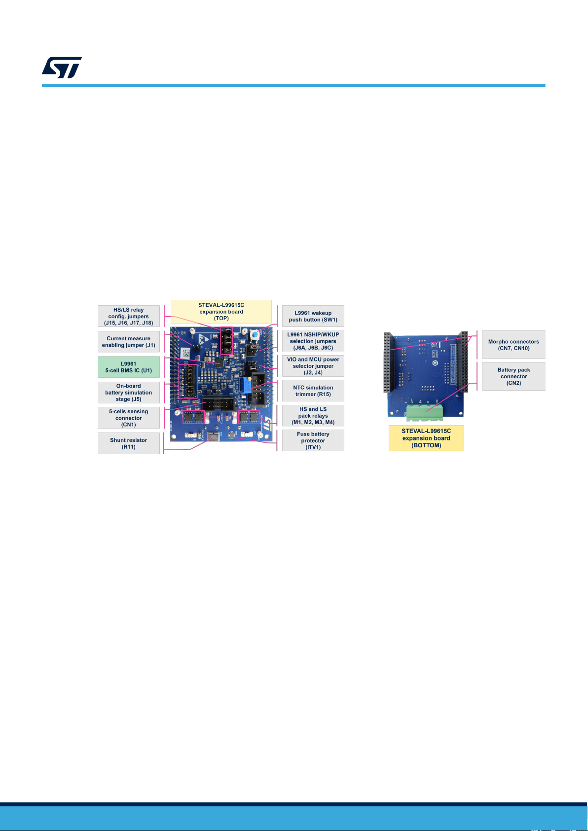
2Jumpers and connectors
2.1 L9961 demo board jumpers and connectors
Table 1. L9961 demo board jumpers and connectors description
Name Description Configuration Type
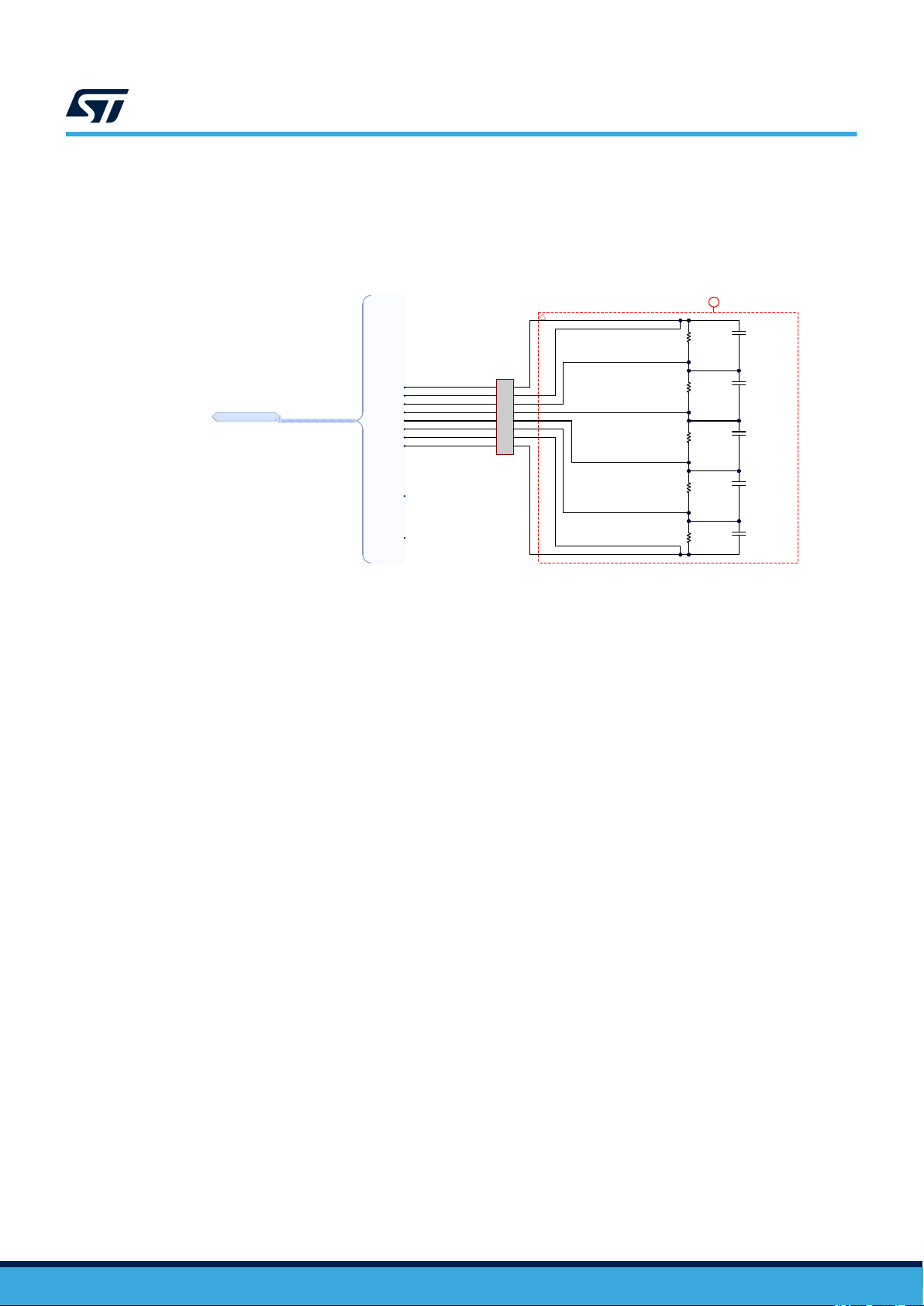
CN1 Remote sense: used to route sense signals from
the 5-cell battery board to the L9961 demo board -10-pin IDC
style
CN2 Battery pack: used to route the power signals from
the 5-cell battery board to the L9961 demo board -
4-pin
Phoenix
header
CN3 Total phase: used to connect an Aardvark I2C/SPI
Host Adapter or a Beagle I2C/SPI Protocol Analyzer -10-pin IDC
style
CN7,
CN10
ST morpho connector: used to place L9961 demo
board on top of the NUCLEO-G071RB micro board - -
J1 Used to measure current flowing into VB pin - -
J2 VIO voltage selector 1-2: 3.3 V from micro
2-3: 3.3 V from L9961 (VREG) -
J4 Used to select micro power source
OPEN: micro is fed from the NUCLEO-
G071RB micro board USB
CLOSE: micro is fed from VREG.
Note: If μC is fed from VREG,
JP3 jumper must be open on
the NUCLEO-G071RB micro
board
-
J5 Battery simulator: used to simulate battery pack
OPEN: battery simulator circuit is
disconnected.
Note: This configuration is used
when the 5-cell battery board
is connected
CLOSED: battery simulator circuit is
connected
Multiple
position
jumper
J6A Used to connect NSHIP pin to B+ - -
J6B Used to drive NSHIP pin from micro - -
J6C Used to drive WAKEUP pin from SW1 push button - -
J13, J14 Used to bypass the HS relay MOSFETs OPEN: when HS relay MOSFETs is used
CLOSED: when LS relay MOSFETs is used
Soldered
jumper
J19, J20 Used to bypass the LS relay MOSFETs OPEN: when LS relay MOSFETs is used
CLOSED: when HS relay MOSFETs is used
Soldered
jumper
J15,
J16,
J17, J18
Used to configure the relay MOSFETs to either high
or low-side usage
1-2: HS configuration is selected
2-3: LS configuration is used -
SW1
Push button: used to take the device out of
SHIPMENT state
Note: If J6C jumper is closed, the SW1
is also used to take the device out
of STADNBY state.
- -
UM3151
Jumpers and connectors
UM3151 - Rev 1 page 8/30