ST STM320518-EVAL User manual

May 2012 Doc ID 023059 Rev 1 1/52
UM1537
User manual
STM320518-EVAL evaluation board
Introduction
The STM320518-EVAL evaluation board is designed as a complete demonstration and
development platform for STMicroelectronic's ARM cortex-M0 core-based
STM32F051R8T6 microcontroller. It features two I2Cs, two SPIs, two USARTs, a 12-bit
ADC, a 12-bit DAC, two GP comparators, internal 8 KB SRAM and 64 KB Flash, touch
sensing, CEC and SWD debugging support.
The full range of hardware features on the board is able to help you evaluate all peripherals
(motor control connector, RS-232, RS-485, audio DAC, linear sensor, microphone ADC,
TFT LCD, IrDA, IR LED, IR receiver, LDR, MicroSD card, CEC on two HDMI connectors, RF
E2PROM, temperature sensor and so on) and develop your own applications. Extension
headers make it possible to easily connect a daughterboard or wrapping board for your
specific application.
An ST-LINK/V2 is integrated on the board as an embedded in-circuit debugger and
programmer for the STM32 MCU.
Figure 1. STM320518-EVAL evaluation board
Table 1. Applicable tools
Type Part number
Evaluation tools STM320518-EVAL
www.st.com

Contents UM1537
2/52 Doc ID 023059 Rev 1
Contents
1 Overview . . . . . . . . . . . . . . . . . . . . . . . . . . . . . . . . . . . . . . . . . . . . . . . . . . 6
1.1 Features . . . . . . . . . . . . . . . . . . . . . . . . . . . . . . . . . . . . . . . . . . . . . . . . . . . 6
1.2 Demonstration software . . . . . . . . . . . . . . . . . . . . . . . . . . . . . . . . . . . . . . . 6
1.3 Order code . . . . . . . . . . . . . . . . . . . . . . . . . . . . . . . . . . . . . . . . . . . . . . . . . 6
1.4 Delivery recommendations . . . . . . . . . . . . . . . . . . . . . . . . . . . . . . . . . . . . . 7
2 Hardware layout and configuration . . . . . . . . . . . . . . . . . . . . . . . . . . . . . 8
2.1 Development and debug support . . . . . . . . . . . . . . . . . . . . . . . . . . . . . . . 10
2.2 Power supply . . . . . . . . . . . . . . . . . . . . . . . . . . . . . . . . . . . . . . . . . . . . . . 11
2.3 Clock source . . . . . . . . . . . . . . . . . . . . . . . . . . . . . . . . . . . . . . . . . . . . . . . 13
2.4 Reset source . . . . . . . . . . . . . . . . . . . . . . . . . . . . . . . . . . . . . . . . . . . . . . 13
2.5 Boot option . . . . . . . . . . . . . . . . . . . . . . . . . . . . . . . . . . . . . . . . . . . . . . . . 14
2.6 Audio . . . . . . . . . . . . . . . . . . . . . . . . . . . . . . . . . . . . . . . . . . . . . . . . . . . . 14
2.7 RS-232, RS-485 and IrDA . . . . . . . . . . . . . . . . . . . . . . . . . . . . . . . . . . . . 15
2.8 Linear sensor . . . . . . . . . . . . . . . . . . . . . . . . . . . . . . . . . . . . . . . . . . . . . . 16
2.9 MicroSD card . . . . . . . . . . . . . . . . . . . . . . . . . . . . . . . . . . . . . . . . . . . . . . 16
2.10 Analog input . . . . . . . . . . . . . . . . . . . . . . . . . . . . . . . . . . . . . . . . . . . . . . . 16
2.11 LDR (light dependent resistor) . . . . . . . . . . . . . . . . . . . . . . . . . . . . . . . . . 16
2.12 Temperature sensor . . . . . . . . . . . . . . . . . . . . . . . . . . . . . . . . . . . . . . . . . 17
2.13 Display and input devices . . . . . . . . . . . . . . . . . . . . . . . . . . . . . . . . . . . . . 17
2.14 RF E2PROM . . . . . . . . . . . . . . . . . . . . . . . . . . . . . . . . . . . . . . . . . . . . . . 18
2.15 HDMI CEC . . . . . . . . . . . . . . . . . . . . . . . . . . . . . . . . . . . . . . . . . . . . . . . . 18
2.16 IR LED and IR receiver . . . . . . . . . . . . . . . . . . . . . . . . . . . . . . . . . . . . . . 19
2.17 Motor control . . . . . . . . . . . . . . . . . . . . . . . . . . . . . . . . . . . . . . . . . . . . . . 19
3 Connector . . . . . . . . . . . . . . . . . . . . . . . . . . . . . . . . . . . . . . . . . . . . . . . . 22
3.1 Motor control connector CN1 . . . . . . . . . . . . . . . . . . . . . . . . . . . . . . . . . . 22
3.2 RF E2PROM connector CN2 . . . . . . . . . . . . . . . . . . . . . . . . . . . . . . . . . . 23
3.3 HDMI sink connector CN3 . . . . . . . . . . . . . . . . . . . . . . . . . . . . . . . . . . . . 23
3.4 HDMI source connector CN4 . . . . . . . . . . . . . . . . . . . . . . . . . . . . . . . . . . 24
3.5 Daughterboard extension connector CN5 and CN6 . . . . . . . . . . . . . . . . . 24

UM1537 Contents
Doc ID 023059 Rev 1 3/52
3.6 RS-232 and RS-485 connector CN7 . . . . . . . . . . . . . . . . . . . . . . . . . . . . 27
3.7 Analog input connector CN8 . . . . . . . . . . . . . . . . . . . . . . . . . . . . . . . . . . 28
3.8 High density SWD connector CN9 . . . . . . . . . . . . . . . . . . . . . . . . . . . . . . 28
3.9 Standard SWD connector CN10 . . . . . . . . . . . . . . . . . . . . . . . . . . . . . . . 29
3.10 Audio jack CN11 . . . . . . . . . . . . . . . . . . . . . . . . . . . . . . . . . . . . . . . . . . . . 29
3.11 ST-LINK/V2 programming connector CN12 . . . . . . . . . . . . . . . . . . . . . . . 29
3.12 ST-LINK/V2 USB type B connector CN13 . . . . . . . . . . . . . . . . . . . . . . . . 29
3.13 MicroSD connector CN14 . . . . . . . . . . . . . . . . . . . . . . . . . . . . . . . . . . . . . 30
3.14 Power connector CN15 . . . . . . . . . . . . . . . . . . . . . . . . . . . . . . . . . . . . . . 31
4 Board schematics . . . . . . . . . . . . . . . . . . . . . . . . . . . . . . . . . . . . . . . . . . 32
Appendix A STM320518-EVAL I/O assignments . . . . . . . . . . . . . . . . . . . . . . . . . 47
Appendix B Mechanical dimensions. . . . . . . . . . . . . . . . . . . . . . . . . . . . . . . . . . . 50
Revision history . . . . . . . . . . . . . . . . . . . . . . . . . . . . . . . . . . . . . . . . . . . . . . . . . . . . 51

List of tables UM1537
4/52 Doc ID 023059 Rev 1
List of tables
Table 1. Applicable tools. . . . . . . . . . . . . . . . . . . . . . . . . . . . . . . . . . . . . . . . . . . . . . . . . . . . . . . . . . . 1
Table 2. Third-party toolchain support . . . . . . . . . . . . . . . . . . . . . . . . . . . . . . . . . . . . . . . . . . . . . . . 10
Table 3. Power source related jumpers . . . . . . . . . . . . . . . . . . . . . . . . . . . . . . . . . . . . . . . . . . . . . . 11
Table 4. Power mode related jumpers . . . . . . . . . . . . . . . . . . . . . . . . . . . . . . . . . . . . . . . . . . . . . . . 12
Table 5. 8 MHz crystal X1 related solder bridges . . . . . . . . . . . . . . . . . . . . . . . . . . . . . . . . . . . . . . . 13
Table 6. 32 kHz crystal X2 related solder bridges . . . . . . . . . . . . . . . . . . . . . . . . . . . . . . . . . . . . . . 13
Table 7. Boot related switch . . . . . . . . . . . . . . . . . . . . . . . . . . . . . . . . . . . . . . . . . . . . . . . . . . . . . . . 14
Table 8. Boot0 related jumpers. . . . . . . . . . . . . . . . . . . . . . . . . . . . . . . . . . . . . . . . . . . . . . . . . . . . . 14
Table 9. Audio related jumpers. . . . . . . . . . . . . . . . . . . . . . . . . . . . . . . . . . . . . . . . . . . . . . . . . . . . . 14
Table 10. RS-232 and IrDA related jumpers. . . . . . . . . . . . . . . . . . . . . . . . . . . . . . . . . . . . . . . . . . . . 15
Table 11. RS-485 related solder bridges . . . . . . . . . . . . . . . . . . . . . . . . . . . . . . . . . . . . . . . . . . . . . . 16
Table 12. LCD modules . . . . . . . . . . . . . . . . . . . . . . . . . . . . . . . . . . . . . . . . . . . . . . . . . . . . . . . . . . . 17
Table 13. Motor control related jumpers . . . . . . . . . . . . . . . . . . . . . . . . . . . . . . . . . . . . . . . . . . . . . . . 21
Table 14. Motor control connector CN1 . . . . . . . . . . . . . . . . . . . . . . . . . . . . . . . . . . . . . . . . . . . . . . . 22
Table 15. RF E2PROM connector CN2 . . . . . . . . . . . . . . . . . . . . . . . . . . . . . . . . . . . . . . . . . . . . . . . 23
Table 16. HDMI sink connector CN3 . . . . . . . . . . . . . . . . . . . . . . . . . . . . . . . . . . . . . . . . . . . . . . . . . 24
Table 17. HDMI source connector CN4 . . . . . . . . . . . . . . . . . . . . . . . . . . . . . . . . . . . . . . . . . . . . . . . 24
Table 18. Daughterboard extension connector CN5 . . . . . . . . . . . . . . . . . . . . . . . . . . . . . . . . . . . . . 25
Table 19. Daughterboard extension connector CN6 . . . . . . . . . . . . . . . . . . . . . . . . . . . . . . . . . . . . . 26
Table 20. RS-232 and RS-485 connector CN7 . . . . . . . . . . . . . . . . . . . . . . . . . . . . . . . . . . . . . . . . . 27
Table 21. Analog input-output connector CN8 . . . . . . . . . . . . . . . . . . . . . . . . . . . . . . . . . . . . . . . . . . 28
Table 22. High density SWD debugging connector CN9 . . . . . . . . . . . . . . . . . . . . . . . . . . . . . . . . . . 28
Table 23. Standard SWD debugging connector CN10 . . . . . . . . . . . . . . . . . . . . . . . . . . . . . . . . . . . . 29
Table 24. USB type B connector CN13 . . . . . . . . . . . . . . . . . . . . . . . . . . . . . . . . . . . . . . . . . . . . . . . 30
Table 25. MicroSD connector CN14 . . . . . . . . . . . . . . . . . . . . . . . . . . . . . . . . . . . . . . . . . . . . . . . . . . 30
Table 26. STM32F051R8T6 MCU pin assignments . . . . . . . . . . . . . . . . . . . . . . . . . . . . . . . . . . . . . . 47
Table 27. Mechanical dimensions . . . . . . . . . . . . . . . . . . . . . . . . . . . . . . . . . . . . . . . . . . . . . . . . . . . 50
Table 28. Document revision history . . . . . . . . . . . . . . . . . . . . . . . . . . . . . . . . . . . . . . . . . . . . . . . . . 51

UM1537 List of figures
Doc ID 023059 Rev 1 5/52
List of figures
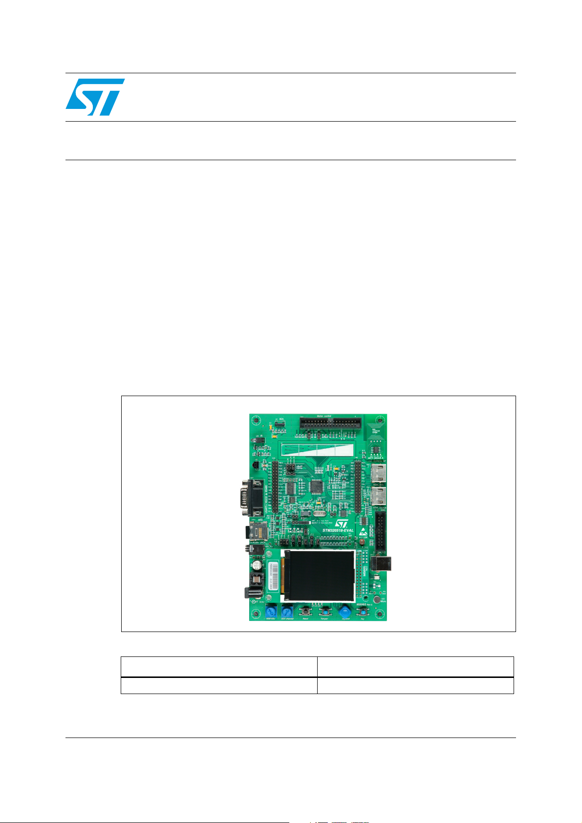
Figure 1. STM320518-EVAL evaluation board . . . . . . . . . . . . . . . . . . . . . . . . . . . . . . . . . . . . . . . . . . 1
Figure 2. Hardware block diagram . . . . . . . . . . . . . . . . . . . . . . . . . . . . . . . . . . . . . . . . . . . . . . . . . . . . 8
Figure 3. STM320518-EVAL evaluation board layout . . . . . . . . . . . . . . . . . . . . . . . . . . . . . . . . . . . . . 9
Figure 4. STM320518-EVAL evaluation board . . . . . . . . . . . . . . . . . . . . . . . . . . . . . . . . . . . . . . . . . 17
Figure 5. STM320518-EVAL evaluation board motor control PCB reworks . . . . . . . . . . . . . . . . . . . 20
Figure 6. Motor control connector CN1 . . . . . . . . . . . . . . . . . . . . . . . . . . . . . . . . . . . . . . . . . . . . . . . 22
Figure 7. RF EEPROM daughterboard connector CN2 . . . . . . . . . . . . . . . . . . . . . . . . . . . . . . . . . . . 23
Figure 8. HDMI sink connector CN3 . . . . . . . . . . . . . . . . . . . . . . . . . . . . . . . . . . . . . . . . . . . . . . . . . 23
Figure 9. HDMI source connector CN4 . . . . . . . . . . . . . . . . . . . . . . . . . . . . . . . . . . . . . . . . . . . . . . . 24
Figure 10. RS-232 and RS-485 connector . . . . . . . . . . . . . . . . . . . . . . . . . . . . . . . . . . . . . . . . . . . . . 27
Figure 11. Analog input-output connector CN8 . . . . . . . . . . . . . . . . . . . . . . . . . . . . . . . . . . . . . . . . . . 28
Figure 12. High density SWD debugging connector CN9 . . . . . . . . . . . . . . . . . . . . . . . . . . . . . . . . . . 28
Figure 13. Standard SWD debugging connector CN10 . . . . . . . . . . . . . . . . . . . . . . . . . . . . . . . . . . . . 29
Figure 14. USB type B connector CN13 . . . . . . . . . . . . . . . . . . . . . . . . . . . . . . . . . . . . . . . . . . . . . . . 30
Figure 15. MicroSD connector CN14 . . . . . . . . . . . . . . . . . . . . . . . . . . . . . . . . . . . . . . . . . . . . . . . . . . 30
Figure 16. Power supply connector CN15 . . . . . . . . . . . . . . . . . . . . . . . . . . . . . . . . . . . . . . . . . . . . . . 31
Figure 17. STM320518-EVAL . . . . . . . . . . . . . . . . . . . . . . . . . . . . . . . . . . . . . . . . . . . . . . . . . . . . . . . 33
Figure 18. MCU . . . . . . . . . . . . . . . . . . . . . . . . . . . . . . . . . . . . . . . . . . . . . . . . . . . . . . . . . . . . . . . . . . 34
Figure 19. Audio. . . . . . . . . . . . . . . . . . . . . . . . . . . . . . . . . . . . . . . . . . . . . . . . . . . . . . . . . . . . . . . . . . 35
Figure 20. HDMI_CEC . . . . . . . . . . . . . . . . . . . . . . . . . . . . . . . . . . . . . . . . . . . . . . . . . . . . . . . . . . . . . 36
Figure 21. LCD and micro SD card . . . . . . . . . . . . . . . . . . . . . . . . . . . . . . . . . . . . . . . . . . . . . . . . . . . 37
Figure 22. Peripherals . . . . . . . . . . . . . . . . . . . . . . . . . . . . . . . . . . . . . . . . . . . . . . . . . . . . . . . . . . . . . 38
Figure 23. RS-232, RS-485 and IrDA . . . . . . . . . . . . . . . . . . . . . . . . . . . . . . . . . . . . . . . . . . . . . . . . . 39
Figure 24. Temperature sensor and RF EEPROM . . . . . . . . . . . . . . . . . . . . . . . . . . . . . . . . . . . . . . . 40
Figure 25. Linear sensor . . . . . . . . . . . . . . . . . . . . . . . . . . . . . . . . . . . . . . . . . . . . . . . . . . . . . . . . . . . 41
Figure 26. ST-LINK/V2 (SWD only) . . . . . . . . . . . . . . . . . . . . . . . . . . . . . . . . . . . . . . . . . . . . . . . . . . . 42
Figure 27. SWD . . . . . . . . . . . . . . . . . . . . . . . . . . . . . . . . . . . . . . . . . . . . . . . . . . . . . . . . . . . . . . . . . . 43
Figure 28. Motor control. . . . . . . . . . . . . . . . . . . . . . . . . . . . . . . . . . . . . . . . . . . . . . . . . . . . . . . . . . . . 44
Figure 29. Power . . . . . . . . . . . . . . . . . . . . . . . . . . . . . . . . . . . . . . . . . . . . . . . . . . . . . . . . . . . . . . . . . 45
Figure 30. 2.4 inch LCD module . . . . . . . . . . . . . . . . . . . . . . . . . . . . . . . . . . . . . . . . . . . . . . . . . . . . . 46
Figure 31. Mechanical dimensions . . . . . . . . . . . . . . . . . . . . . . . . . . . . . . . . . . . . . . . . . . . . . . . . . . . 50

Overview UM1537
6/52 Doc ID 023059 Rev 1
1 Overview
1.1 Features
●Three 5 V power supply options: power jack, ST-LINK/V2 USB connector or
daughterboard
●Audio speaker and microphone connected to DAC and ADC of STM32F051R8T6
●2 Gbyte or more SPI interface MicroSD card
●I2C compatible serial interface temperature sensor
●RF E2PROM
●RS-232 and RS-485 communication
●IrDA transceiver
●IR LED and IR receiver
●SWD debug support, ST-LINK/V2 embedded
●240 x 320 TFT color LCD connected to SPI interface of STM32F051R8T6
●Joystick with 4-direction control and selector
●Reset, tamper and user buttons
●4 color LEDs
●Extension connector for daughterboard or wrapping board
●MCU voltage choice fixed at 3.3 V or adjustable from 2 to 3.6 V
●Linear sensor
●Light dependent resistor (LDR)
●Potentiometer
●Two HDMI connectors with DDC and CEC
●Motor control connector
●Boards RoHS compliant (lead free)
1.2 Demonstration software
Demonstration software is preloaded in the board's Flash memory for easy demonstration of
the device peripherals in stand-alone mode. For more information and to download the
latest version available, refer to the STM320518-EVAL demonstration software available at
www.st.com.
1.3 Order code
To order the STM32F051R8T6 evaluation board, use the order code STM320518-EVAL.

UM1537 Overview
Doc ID 023059 Rev 1 7/52
1.4 Delivery recommendations
Some verifications are needed before using the board for the first time to make sure that
nothing has been damaged during shipment and that no components are unplugged or lost.
When the board is extracted from its plastic bag, please check that no component remains
in the bag.
The main components to verify are:
1. The 8 MHz crystal (X1) which may have been removed from its socket by a shock.
2. The MicroSD card which may have been ejected from the connector CN14 (left side of
the board).
3. The dual interface EEPROM board (ANT7-M24LR-A) which may have been unplugged
from the connector CN2 (top right corner of the board).

Hardware layout and configuration UM1537
8/52 Doc ID 023059 Rev 1
2 Hardware layout and configuration
The STM320518-EVAL evaluation board is designed around the STM32F051R8T6 (64-pin
LQFP package). The hardware block diagram shown in Figure 2 illustrates the connection
between the STM32F051R8T6 and peripherals (motor control connector, RS-232, RS-485,
audio DAC, linear sensor, microphone ADC, TFT LCD, IrDA, IR LED, IR receiver, LDR,
MicroSD card, CEC and DDC on two HDMI connectors, RF E2PROM and temperature
sensor and so on). Figure 3 shows where you can locate these features on the evaluation
board.
Figure 2. Hardware block diagram
34-&24
23
TRANSCEIVER
)R$!
TRANSCEIVER
6REGULATOR
#OLOR,#$
-ICRO3$
CARD
3PEAKER
!MPLIFIER
($-)SINK
,%$S
0OTENTIOMETER
2323
$"CONNECTOR
$!#
'0)/
)#
%XTENSION
CONNECTORFOR
'0)/S
53!24
4EMPERATURE
SENSOR 37$
*OYSTICK
6TO6
ADJUSTABLE
REGULATOR
!$#
%MBEDDED
34,).+6
53"4YPE"
CONNECTOR
-ICRO0HONE
!MPLIFIER
4AMPER
BUTTON
)2/54
2&
%%02/-
6POWER
SWITCH
#%#
*4!'37$
CONNECTOR
23
TRANSCEIVER
30)
,INEAR
SENSOR 43#ONTROLLER
,$2 #-0?).P
6REGULATOR
($-)
SOURCE
)2,%$
)2RECEIVER4)-?#(
-OTORCONTROL
CONNECTOR
)#
6OLTAGE
TRANSLATOR
6OLTAGE
TRANSLATOR
-36

UM1537 Hardware layout and configuration
Doc ID 023059 Rev 1 9/52
Figure 3. STM320518-EVAL evaluation board layout
U22
microphone
CN4
HDMI_Source
connector
CN1
motor control connector
RV3
potentiometer
B1
reset key
CN 2
RF E2PROM
connector
LD5
IR LED
CN7
RS-232/RS-485
connector
CN16
TFT LCD
U1
IrDA transceiver
4 colorsLEDS
LD7
ST-LINK/V2
COM LED
CN3
HDMI_Sink
connector
U2
IR receiver
CN15
power jack
B3
user button
S1
Linear sensor
U21
joystick
B2
tamper button
RV2
VDD_Adjustment
CN13
ST-LINK/V2 USB
connector
CN14
MicroSD Card
U4
STM32F051R8T6
CN11
audio jack
CN10
SWD connector
CN5, CN6
extension header
MS30809V1

Hardware layout and configuration UM1537
10/52 Doc ID 023059 Rev 1
2.1 Development and debug support
Version 2 of the ST-LINK (ST-LINK/V2) is embedded on the board. This tool allows onboard
program loading and debugging of the STM32F051R8T6 using the SWD interface. The
third-party debug tools are also supported by the SWD connector CN10.
A specific driver must be installed on your PC for communication with the embedded ST-
LINK/V2. This driver, called ST-LINK_V2_USBdriver.exe is available on the web. To
download and install this driver, refer to the software and development tools page for the
STM32F0 family on www.st.com.
Third-party toolchains, such as Atollic TrueSTUDIO, Keil MDK-ARM, IAR EWARM and
TASKING VX-toolset for ARM Cortex-M, support ST-LINK/V2 according to Ta ble 2.
The embedded ST-LINK/V2 is connected to the PC via a standard USB cable from
connector CN13. The bicolor LED LD7 (COM) indicates the status of the communication as
follows.
●Slow blinking Red/Off: at power-on before USB initialization.
●Fast blinking Red/Off: after the first correct communication between the PC and ST-
Link/V2 (enumeration).
●Constant Red On: when initialization between the PC and ST-LINK/V2 is successfully
finished.
●Constant Green On: after successful target communication initialization.
●Blinking Red/Green: during communication with the target.
●Red On: communication is finished and OK.
●Orange On: communication failure.
Note: The board can be powered via CN13 (embedded ST/LINK/V2 USB connector) even if an
external tool is connected to CN9 (high density SWD connector) or CN10 (SWD connector).
Table 2. Third-party toolchain support
Manufacturer Toolchain From version...
Atollic TrueSTUDIO 2.1
IAR EWARM 6.20.4
Keil MDK-ARM 4.20
TASKING VX-toolset for ARM Cortex-M 4.0.1

UM1537 Hardware layout and configuration
Doc ID 023059 Rev 1 11/52
2.2 Power supply
The STM320518-EVAL evaluation board is designed to be powered by a 5V DC power
supply and to be protected by PolyZen from incorrect power plug-in events.
It is possible to configure the evaluation board to use any of the following three sources for
the power supply.
●5V DC power adapter connected to CN15, the power jack on the board (power supply
unit (PSU) on the silk screen). External power supply is not provided with the board.
●5V DC power with 500 mA limitation from CN13, the USB type B connector of ST-
LINK/V2 (USB 5 V power source (STlk) on silkscreen).
●5V DC power from CN6, the extension connector for daughterboard (daughterboard
power source (D5V) on silkscreen).
The power source is selected by setting the related jumpers JP8 as described in Ta ble 3 .
Table 3. Power source related jumpers
Jumper Description
JP8
JP8 selects one of the three possible power supply resources.
For the power supply jack (CN15) to STM320518-EVAL only,
JP8 is set as shown:
For power supply from the daughterboard connectors (CN6) to
STM320518-EVAL only, JP8 is set as shown:
For power supply from USB (CN13) of ST-LINK/V2 to STM320518-
EVAL only, JP8 is set as shown (default setting):
For power supply from the power supply jack (CN15) to both
STM320518-EVAL and daughterboard connected on CN5 and CN6,
JP8 is set as shown (the daughterboard must not have its own power
supply connected):
STlk
D5V
PSU
STlk
D5V
PSU
STlk
D5V
PSU
STlk
D5V
PSU

Hardware layout and configuration UM1537
12/52 Doc ID 023059 Rev 1
A total of three power modes are supported on the board and can be configured by setting
the related jumpers JP7, JP9, JP10 and JP11 as described in Tabl e 4 and its related notes.
●Mode1: the VDD and VDDA are connected together and powered by a fixed 3.3 V.
●Mode2: the VDD and VDDA are connected together and powered by an adjustable
voltage ranging from 2.0 V to 3.6 V.
●Mode3: the VDD is powered by an adjustable voltage ranging from 2.0 V to 3.6 V while
VDDA is powered by a fixed 3.3 V.
Note: MCU IDD measurement can be done with a current meter mounted on JP7 when it is open.
Note: Jumper JP11 must be open (to disconnect VDDA from all analog power VDD_ANA which is
connected to the analog circuits on the board) for MCU Idd measurement.
The LED LD6 is lit when the STM320518-EVAL evaluation board is correctly powered by
5V.
JP12
The Vbat pin of STM32F051R8T6 is connected to VDD when JP12 is set
as shown (default setting):
The Vbat pin of STM32F051R8T6 is connected to a 3 V battery when
JP12 is set as shown:
Table 4. Power mode related jumpers
Power mode
Power mode configuration MCU IDD measurement
JP9 JP10
Mode1
OK
Not allowed
Mode2
OK
Mode3
Not allowed
Table 3. Power source related jumpers (continued)
Jumper Description
321
321
321
321
321
321
321
321
321
321

UM1537 Hardware layout and configuration
Doc ID 023059 Rev 1 13/52
2.3 Clock source
Two clock sources are available on the STM320518-EVAL evaluation board for
STM32F051R8T6 and RTC embedded.
●X1, 8 MHz crystal with a socket for the STM32F051R8T6 microcontroller. It can be
removed from the socket when the internal RC clock is used.
●X2, 32 kHz crystal for embedded RTC.
2.4 Reset source
The reset signal of the STM320518-EVAL evaluation board is low active and the reset
sources include the following.
●Reset button B1
●Debugging tools from SWD connector CN10 and CN9
●Daughterboard from CN6
●Embedded ST-LINK/V2
●RS232 connector CN7 for ISP.
Note: The jumper JP6 is to be closed for RESET handled by pin8 of the RS-232 connector CN7
(CTS signal). Refer to Section 2.7 information.
Table 5. 8 MHz crystal X1 related solder bridges
Jumper Description
SB13
PF0 is connected to an 8 MHz crystal when SB13 is open (default setting).
PF0 is connected to an extension connector CN6 when SB13 is closed. In such a
case, C34 and X1 must be removed.
SB14
PF1 is connected to an 8 MHz crystal when SB14 is open (default setting).
PF1 is connected to an extension connector CN6 when SB14 is closed. In such a
case, R59 must be removed to avoid disturbance due to the 8 MHz quartz.
Table 6. 32 kHz crystal X2 related solder bridges
Jumper Description
SB9
PC14 is connected to a 32 kHz crystal when SB9 is open (default setting).
PC14 is connected to an extension connector CN5 when SB9 is closed. In such a
case, R57 must be removed to avoid disturbance due to the 32 kHz quartz.
SB10
PC15 is connected to a 32 kHz crystal when SB10 is open (default setting).
PC15 is connected to an extension connector CN5 when SB10 is closed. In such a
case, R58 must be removed to avoid disturbance due to the 32 kHz quartz.

Hardware layout and configuration UM1537
14/52 Doc ID 023059 Rev 1
2.5 Boot option
The STM320518-EVAL evaluation board can boot from:
●Embedded User Flash
●System memory with boot loader for ISP
●Embedded SRAM for debugging
The boot option is configured by setting switch SW1 (BOOT0) and one Option bit in the
Small Information block (SIF). The BOOT0 can also be configured via the RS-232 connector
CN7.
2.6 Audio
The STM320518-EVAL evaluation board supports a speaker that is connected to the DAC
output of the STM32F051R8T6 through an audio amplifier and microphone, which is in turn
connected to the ADC input of the STM32F051R8T6 through a microphone amplifier. The
speaker can be enabled or disabled by setting JP13 (Ta bl e 9 ).
Table 7. Boot related switch
Switch
configuration
Bit12 in USER
OPTION BYTES Boot source
0 <-> 1
X
STM320518-EVAL boot from User Flash when SW1 and
Bit12 in User OPTION bytes set as shown to the left (default
setting).
0 <-> 1
0STM320518-EVAL boot from Embedded SRAM when SW1
and Bit12 in User OPTION bytes set as shown to the left.
0<-> 1
1STM320518-EVAL boot from System Memory when SW1
and Bit12 in User OPTION bytes set as shown to the left.
Table 8. Boot0 related jumpers
Jumper Description
JP5
The Bootloader_BOOT0 is managed by pin 6 of connector CN7 (RS-232 DSR
signal) when JP5 is closed. This configuration is used for the boot loader application
only.
Default Setting: Not fitted
Table 9. Audio related jumpers
Jumper Description
JP13
Speaker amplifier U17 is enabled when JP13 is open (default setting).
Speaker amplifier U17 is disabled when JP13 is closed.

UM1537 Hardware layout and configuration
Doc ID 023059 Rev 1 15/52
2.7 RS-232, RS-485 and IrDA
The RS-232 (with hardware flow control CTS and RTS), RS-485 and IrDA communication is
supported by D-type 9-pin RS-232/RS-485 connectors CN7, and IrDA transceiver U1 which
is connected to USART1 of the STM32F051R8T6 on the STM320518-EVAL evaluation
board. The signal Bootloader_RESET (shared with the CTS signal) and Bootloader_BOOT0
(shared with the DSR signal) are added to the RS-232 connector CN7 for ISP support.
Table 10. RS-232 and IrDA related jumpers
Jumper Description
JP3
RS232_RX is connected to the RS-232 transceiver and RS-232 communication is
enabled when JP3 is set as shown (default setting):
RS485_RX is connected to the RS-485 transceiver and RS-485 communication is
enabled when JP3 is set as shown:
IrDA_RX is connected to the IrDA transceiver and IrDA communication is enabled
when JP3 is set as shown:
JP4
PA11 is connected to the RS-232 transceiver as RS232_CTS when JP4 is set as
shown (default setting):
PA11 is connected to the HDMI_Sink connector as HPD when JP4 is set as shown:
RS232_RX
RS485_RX
IrDA_RX
RS232_RX
RS485_RX
IrDA_RX
RS232_RX
RS485_RX
IrDA_RX
321
321

Hardware layout and configuration UM1537
16/52 Doc ID 023059 Rev 1
The RS-485 communication is supported by the RS-485 transceiver ST485ABDR, which is
connected to pin4 and pin9 of the D-type 9-pin connectors CN7 (that share the same
connector as USART1).
2.8 Linear sensor
The linear sensor is supported on the STM320518-EVAL evaluation board and connected to
four capacitive sensing channels (PB[11:14]) in group6 with an active shield connected to
two capacitive sensing channels (PC5 and PB0) in group3.
Note: The linear sensor is only fully functional when the STM320518-EVAL is powered on power
mode 1 (both VDD and VDDA are connected to a fixed 3.3 V). It is potentially necessary to
adjust the capacitor value of C14 and C15 and the firmware to adapt them to the voltage
range from 2 V to 3.6 V of VDD on power modes 2 and 3.
2.9 MicroSD card
The 2 GB (or more) MicroSD card connected to the SPI1 port of the STM32F051R8T6 is
available on the board. MicroSD card detection is managed by the standard IO port PB15.
2.10 Analog input
The two-pin header CN8 and 10 kohm potentiometer RV3 are connected to PC1 of the
STM32F051R8T6 as an analog input. A low-pass filter can be implemented by replacing
R60 and C36 with the correct resistor and capacitor values as required by the end-user
application.
2.11 LDR (light dependent resistor)
The VDDA is divided by the resistor bridge of the LDR VT9ON1 and 8.2 K resistor. It is
connected to PA1 (COM1_IN+/ADC IN1) as shown in Figure 4.
Table 11. RS-485 related solder bridges
Jumper Description
SB11,SB12
The external failsafe biasing are enabled when solder bridges SB11 and SB12 are
closed.
Default setting: not fitted
SB8 The bus termination is enabled when solder bridge SB8 is closed.
Default setting: not fitted
SB16
The AC termination is disabled when solder bridge SB16 is closed for high baud rate
communication.
Default setting: not fitted

UM1537 Hardware layout and configuration
Doc ID 023059 Rev 1 17/52
Figure 4. STM320518-EVAL evaluation board
It is possible to compare the LDR output with 1/4 band gap, 1/2 band gap, 3/4 band gap,
band gap and DAC1 OUT, and to connect the LDR output to ADC IN1 for AD conversion.
2.12 Temperature sensor
A temperature sensor STLM75M2E is connected to the I2C1 bus of the STM32F051R8T6. It
shares the same I2C1 bus as the RF E2PROM and DDC on the HDMI_Source connector
CN4.
2.13 Display and input devices
The 2.4 inch color TFT LCD connected to the SPI1 port of the STM32F051R8T6 and four
general-purpose color LEDs (LD 1, 2, 3 and 4) are available as display devices. The
4-direction joystick (U21) with selection key connected to PA0 and support wakeup feature
and tamper button (B2) are available as input devices.
"ANDGAP6
'0#/-0?).
'0#/-0?).
'.$
.#
'0COMPARATOR
0!
,$2
+ !$#).
"ANDGAP
"ANDGAP
¢"ANDGAP
$!#/54
6$$!
-36
Table 12. LCD modules
2.4-inch TFT LCD connector CN16
Pin Description Pin connection Pin Description Pin connection
1CS PF4 9VDD 3.3V
2SCL PA5 10VCI 3.3V
3 SDI PA7 11 GND GND
4RS - 12GND GND
5 WR - 13 BL_VDD 5 V

Hardware layout and configuration UM1537
18/52 Doc ID 023059 Rev 1
Note: The bi-directional voltage translator is implemented on the SPI MOSI signal between the
STM32F051R8T6 and the LCD to support the 3-wire serial interface of the
AM240320LGTNQW-01H LCD panel. The direction of this voltage translator is controlled by
IO PB2 (the IO PA7 acts as MOSI when PB2 is high or as MISO when PB2 is LOW).
2.14 RF E2PROM
An RF E2PROM module ANT7-M24LR-A is mounted on connector CN2 and is connected to
the I2C1 bus of the STM32F051R8T6. It shares the same I2C1 bus as the temperature
sensor U8 and DDC on the HDMI_Source connector CN4.
2.15 HDMI CEC
Two HDMI connectors CN3 and CN4 are available on the STM320518EVAL board.
●Connector CN3 is an HDMI sink connector with:
– DDC connected to I2C2 of the STM32F051R8T6
– HPD controlled by I/O PA11 through transistor T3
– CEC connected to PB10 through transistor T4
●Connector CN4 is an HDMI source connector with:
– DDC connected to I2C1 of the STM32F051R8T6 and shared with the temperature
sensor and RF E2PROM
– HPD controlled by I/O PA8
– CEC connected to PB10 through transistor T4
– 5V HDMI powered by power switch U5
Signals TDMS D+[0,1,2], TDMS_CLK+, TDMS D-[0,1,2] and TDMS_CLK are connected
together on these two HDMI connectors.
CEC injector mode can be enabled by reworking the PCB (for debugging purposes only):
●Remove resistors R63, R66, R23, R62, R68, R51 and R13.
●Close solder bridges SB4, SB5, SB6 and SB7.
Note: The I/O PA11 must be set in open-drain output mode by firmware for HPD signal control on
the HDMI sink connector CN3.
6 RD - 14 BL_Control 5 V
7 SDO PB4 15 BL_GND GND
8 RESET RESET# 16 BL_GND GND
Table 12. LCD modules (continued)
2.4-inch TFT LCD connector CN16
Pin Description Pin connection Pin Description Pin connection

UM1537 Hardware layout and configuration
Doc ID 023059 Rev 1 19/52
2.16 IR LED and IR receiver
The IR receiver TSOP34836 is connected to PB3 of the STM32F051R8T6 and a current
around 100 mA on the IR LED is driven by PB9 through transistors T1 and T2 on the board.
Note: The IR LED may be driven by PB9 directly with a 20 mA current when SB3 is closed and
R11 is removed.
2.17 Motor control
The STM320518-EVAL evaluation board supports both asynchronous and synchronous
three-phase brushless motor control via a 34-pin connector CN1. This connector provides
all required control and feedback signals to and from the motor power-driving board.
Available signals on this connector include emergency stop, motor speed, 3-phase motor
current, bus voltage, heatsink temperature coming from the motor driving board and six
channels of the PWM control signal going to the motor driving circuit.
Some PCB reworks are required for the motor control application to disconnect peripherals
that share IOs with the motor control connector. These IOs need to be connected to the
motor control connector.
●Remove resistors R89, R52, R19, R55, R32, R38, R42, R88, R83, R20, R36, R18 and
R50.
●Mount R25, R29, R30, R39, R4, R35, R37, R44, R22 and R41 with a 0 ohm resistor.
All resistors to be removed are marked in red while resistors to be soldered are marked in
green in Figure 5.

Hardware layout and configuration UM1537
20/52 Doc ID 023059 Rev 1
Figure 5. STM320518-EVAL evaluation board motor control PCB reworks
The RS-232 connector CN7 is re-connected to USART1 on the IOs PB6 and PB7 instead of
PA9 and PA10 for the motor control application.
Table of contents
Other ST Motherboard manuals