PAGE
7
PC BOARD - PC-188 BITBUS I/F FOR IBM-PC
ORDER NO. 5904512211MAY 2002 - REV. 1.2
4.8 Default configuration
Table 4.8.1
Jumper State Function
JS0
JS1
JS2
JS3
JS4
JS5
JS6
JS7
OFF
OFF
OFF
OFF
OFF
OFF
OFF
OFF
00H
00H
00H
00H
00H
00H
00H
00H
set bit 0 of node address
set bit 1 of node address
set bit 2 of node address
set bit 3 of node address
set bit 4 of node address
set bit 5 of node address
set bit 6 of node address
set bit 7 of node address
JF0
JF1
JF2
JF3
JF4
JF5
JF6
ON
OFF
OFF
OFF
OFF
OFF
ON
208H
208H
208H
208H
208H
208H
208H
set bit 3 of PC base address
set bit 4 of PC base address
set bit 5 of PC base address
set bit 6 of PC base address
set bit 7 of PC base address
set bit 8 of PC base address
set bit 9 of PC base address
JA0
JA1
JA2
JA3
JA4
JA5
JA6
JA7
OFF
OFF
OFF
OFF
OFF
OFF
OFF
OFF
Select a speed af 375 Kbps
not used
not used
not used
not used
not used
Fully compatible with 8044 Intel
Dynamic configuration disabled
JQ3
JQ4
JQ5
JQ6
JQ7
JQ9
JQ10
JQ11
JQ12
JQ14
JQ15
OFF
OFF
OFF
OFF
OFF
OFF
OFF
OFF
OFF
OFF
OFF
1-2 connect IRQ3 when transmission is interrupted (PC-188)
2-3 connect IRQ3 when reception is interrupted (PC)
Connect IRQ4 to TINT (1-2) or RTINT (2-3)
Connect IRQ5 to TINT (1-2) or RTINT (2-3)
Connect IRQ6 to TINT (1-2) or RTINT (2-3)
Connect IRQ7 to TINT (1-2) or RTINT (2-3)
Connect IRQ9 to TINT (1-2) or RTINT (2-3)
Connect IRQ10 to TINT (1-2) or RTINT (2-3)
Connect IRQ11 to TINT (1-2) or RTINT (2-3)
Connect IRQ12 to TINT (1-2) or RTINT (2-3)
Connect IRQ14 to TINT (1-2) or RTINT (2-3)
Connect IRQ15 to TINT (1-2) or RTINT (2-3)
J3
J2
J6
J4
J16
J17
J7
J8
J9
J10
J11
J12
J13
ON
OFF
OFF
ON
1-2
OFF
1-2
1-2
1-2
1-2
1-2
1-2
1-2
Select RAM up to 128K×8
Select RAM up to 128K×8
Select EPROM
Select EPROM
Select EPROM
Enable Slot#0 operation
JT1
JT2
ON
ON
Terminals connected to DATA line
Terminals connected to RTS line
Join connector XP1 in parallel
to connector XS1.
If jumpers are moved to position 2-3
XP1 will be connected to Slot#1
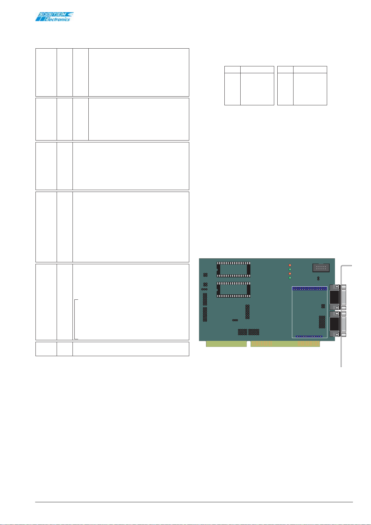
4.9 Bitbus network connectors
Two DB-9 connectors (at the input and output of the
line) are provided to connect the board to the Bitbus
network (the pinout is identified as shown in Table 4.9.1).
Table 4.9.1 Pinout of the Bitbus network connectors.
The Bitbus network cable should have the DATA/DATA-
signal pairs and RTS/RTS- twisted and shielded together
with the RGND line as shown in Figures 1.3 and 1.4.
By moving jumpers J7…J12 from location 1-2 (normal)
to position 2-3 (slot#0), the 9-pin male connector XP1
is disconnected from the Bitbus network and joined to
the piggy-back module (optional) placed in slot#0. As a
result, an additional serial interface (RS232, RS422,
RS485 or CAN) is available. By using rectangular
connector XP2, and RS232 interface is always available.
The latter may be used by sending the SYSTEM Electronics
commands defined (Open, Send, Receive, Close) to task
GBS (ex RAC). As an alternative, the library functions of
an application program can be used for the same
purpose. This serial port may also be used for debugging
(at source level) application programs (with tools
provided by SYSTEM Electronics or other manufacturers).
Figure 4.9.1 Jumper location.
SIGNAL SIGNAL
PIN PIN
1
2
3
4
5
6
7
8
9
--
GND
DATA-
RTS-
RGND
--
GND
DATA
RTS
RAM
SLOT *0
EXPANSION SLOT
XP1
RAM1MJ3
RAM4MJ2 EPROM/FLASH
XP2
RL
GL
SER
+5V
XS1
J3
J2
J6
J4
J16
JF0
JF1
2
3
4
5
6
JF
JF
JF
JF
JF
JA0
JA1
2
3
4
5
6
JA7
JA
JA
JA
JA
JA
JS0
JS1
2
3
4
5
6
JS7
JS
JS
JS
JS
JS J12
J13
J11
J9
J10
J8
J7
JQ9
JQ7
JQ6
JQ5
JQ4
JQ3
JQ10
JQ11
JQ12
JQ15
JQ14
JT1
JT2 NORMAL
SLOT*0
1
1
1
J14
J17
Tint
Rint
TERM
1