manuals.online logo
Brands
  1. Home
  2. •
  3. Brands
  4. •
  5. Tektronix
  6. •
  7. Test Equipment
  8. •
  9. Tektronix TDS 520 Operating instructions

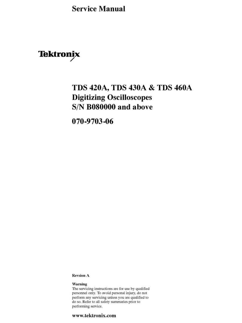
Tektronix TDS 520 Operating instructions

1---
WARNING I
The following servicing instructions
are for use by qualified service
personnel only.
To
avoid personal
injury,
do
not perform any servicing
unless you are qualified
to
do
so.
Refer
to
the Safety Summary prior
to
performing any service.
Please
check
for
CHANGE INFORMATION
at
the
rear
of
this
manual.
Part No. 070-8313-00
Product Group 55
lHE
TDS520
DIGITIZING
OSCILLOSCOPE
Component Level
Diagnostic and
Repair Manual
Volume 2
COMMITTED
TO
EJCCEL1.ENCE
DIGITALY REMASTERED
OUT OF PRINT- MANUAL SCAN
S
By
ArtekMedia
P.O. BOX 175
Welch, MN 55089-0175
Phone: 651-269-4265
www.artekmedia.com
“High resolution scans of obsolete technical manuals”
If you are looking for a quality scanned technical manual in PDF format please visit our WEB
site at www.artekmedia.com or drop us an email at manuals@artekmedia.com
If you don’t see the manual you need on the list drop us a line anyway we may still be able to
obtain the manual you need or direct you to other sources. If you have an existing manual you
would like scanned please write for details. This can often be done very reasonably in
consideration for adding your manual to our library.
Typically the scans in our manuals are done as follows;
1) Typed text pages are typically scanned in black and white at 300 dpi.
2) Photo pages are typically scanned in gray scale mode at 600 dpi
3) Schematic diagram pages are typically scanned in black and white at 600
dpi unless the original manual had colored high lighting (as is the case for
some 70’s vintage Tektronix manuals).
4) Most manuals are text searchable
5) All manuals are fully bookmarked
All data is guaranteed for life (yours or mine …whichever is shorter). If for ANY REASON your
file becomes corrupted, deleted or lost, ArtekMedia will replace the file for the priceof shipping,
or free via FTP download.
Thanks
Dave & Lynn Henderson
ArtekMedia
,.---
WARRANTY
Tektronix warrants that this product will be free from defects
in
materials and workmanship for a period of three
(3)
years
from the date of shipment. If any such product proves defective during this warranty period, Tektronix,
at
its option, either
will repair the defective product without charge for parts and labor. or will provide a replacement in exchange for the
defective product.
In
order to obtain service under this warranty, Customer must notify Tektronix of the defect before the expiration of the
warranty period and make suitable arrangements for the performance of service. Customer shall be responsible for
packaging and shipping the defective product to the service center designated by Tektronix, with shipping charges
prepaid. Tektronix shall pay for the return of the product to Customer if the shipment is to a location within the country
in
which the Tektronix service center is located. Customer shall be responsible for paying all shipping charges. duties. taxes.
and any other charges for products returned to any other locations.
This warranty shall not apply to any defect, failure or damage caused by improper use or improper
or
inadequate
maintenance and care. Tektronix shall not be obligated to furnish service under this warranty
a)
to
repair damage resulting
from attempts
by
personnel other than Tektronix representatives to install, repair
or
service the product;
b)
to repair
damage resulting from improper use
or
connection to incompatible equipment; or c) to service a product that has been
modified
or
integrated with other products when the effect
of
such modification or integration increases the time or
difficulty
of
servicing the product.
THIS WARRANTY
IS
GIVEN
BY
TEKTRONIX WITH RESPECT TO THIS PRODUCT IN LIEU OF ANY OTHER
WARRANTIES, EXPRESS OR IMPLIED. TEKTRONIX AND ITS VENDORS DISCLAIM ANY IMPLIED WARRANTIES
OF MERCHANTABILITY
OR
FITNESS FOR A PARTICULAR PURPOSE. TEKTRONIX' RESPONSIBILITY TO REPAIR
OR
REPLACE DEFECTIVE PRODUCTS IS THE SOLE AND EXCLUSIVE REMEDY PROVIDED TO THE CUSTOMER
FOR BREACH
OF
THIS
WARRANTY. TEKTRONIX AND ITS VENDORS WILL
NOT
BE
LIABLE FOR ANY INDIRECT,
SPECIAL, INCIDENTAL,
OR
CONSEQUENTIAL DAMAGES IRRESPECTIVE OF WHETHER TEKTRONIX
OR
THE
VENDOR
HAS
ADVANCE NOTICE OF THE POSSIBILITY OF SUCH DAMAGES.
Instrument Serial Numbers
Each instrument manufactured
by
Tektronix has a serial number
on
a panel insert or tag, or stamped on the
chassis. The first letter
in
the serial number designates the country of manufacture. The last five digits of the
serial number are assigned sequentially and are unique to each instrument. Those manufactured
in
the United
States have six unique digits. The country of manufacture is identified as follows:
B010000
E200000
J300000
H700000
Tektronix, Inc., Beaverton, Oregon,
USA
Tektronix United Kingdom, Ltd., London
SonyfTektronix, Japan
Tektronix Holland,
NV,
Heerenveen,
The
Netherlands
Instruments manufactured for Tektronix
by
external vendors outside the United States
are
assigned a two digit
alpha code to identify the country of manufacture (e.g., JP for Japan,
HK
for Hong Kong, IL for Israel, etc.).
Tektronix, Inc.,
P.O.
Box 500, Beaverton,
OR
97077
Printed
in
U.S.A.
Copyright © Tektronix, Inc., 1991. All rights reserved. Tektronix products are covered
by
U.S.
and foreign
patents, issued and pending. The following are registered trademarks:
TEKTRONIX,
TEK,
TEKPROBE, SCOPEMOBILE and
~
~
Deskjet, HPGL, Laserjet and Thinkjet
are
products of the Hewlett-Packard Company.
Epson is a registered trademark of Epson America, Inc.
Interleaf is a trademark of Interleaf, Inc.
PostScript is a registered trademark of Adobe Systems, Inc.
'-:-,'
-
.~"'.
Vol.
2 Figure
i:
Semiconductor Lead Configurations . . . . . . . . . . . . . . . . . . . . . . . . . . . . . . .
..
Vol.
2
iv
Vol.
2 Figure ii: Locating Components
on
Circuit Board
or
Schematic
Diagram.
. . . . . . . . . .
Vol.
2 v
A10 Acquisition
Vol. 2 Figure
9-1:
Attenuator Programming
........................................
.
Vol.
2
9-1
Vol. 2 Figure 9-2: A
15
Attenuator Board Programming Troubleshooting Procedure
........
.
Vol.
2
9-1
Vol. 2 Figure 9-3: Acquisition Digital Control Troubleshooting Procedure
................
.
Vol.
2
9-2
Vol. 2 Figure 9-4: Acquisition
ProcPs~or
fro.Jbleshooting Procedure
...................
.
Vol.
2
9-4
Vol. 2 Figure 9-5: Nonnal
Path
of the Vertical Channels
..............................
.
Vol.
2
9-5
Vol. 2 Figure 9-6:
ND
Converter Troubleshooting Procedure
..........................
.
Vol.
2
9-5
Vol. 2 Figure 9-7: Analog
DAC
Control Troubleshooting Procedure
....................
.
Vol.
2 9-6
Vol. 2 Figure 9-8:
Pin
6 of U931.
U932. U933.
and U934
.............................
.
Vol.
2
9-7
Vol. 2 Figure 9-9:
TP903
(PCO)
..................................................
.
Vol.
2
9-7
Vol. 2 Figure 9-10:
TP906
(PC3). .
...............................................
.
Vol.
2
9-7
Vol. 2 Figure 9-11:
TP909
......................................................
.
Vol.
2
9-7
Vol. 2 Figure 9-12:
TP911
......................................................
.
Vol.
2
9-7
Vol. 2 Figure 9-13:
TP904
(PC1)
.................................................
.
Vol.
2
9-7
Vol. 2 Figure 9-14:
TP911
......................................................
.
Vol.
2
9-8
Vol. 2 Figure 9-15:
TP912
......................................................
.
Vol.
2
9-8
Vol. 2 Figure 9-16:
TP904
(PC1)
.................................................
.
Vol.
2
9-8
Vol. 2 Figure 9-17:
TP905
(PC2)
.................................................
.
Vol.
2
9-8
Vol. 2 Figure 9-18:
U601
pin 3
(PC7)
.............................................
.
Vol.
2
9-8
Vol. 2 Figure 9-19: Analog Holdoff
Trou~!~shC'oting
Procedure
........................
.
Vol.
2
9-9
Vol. 2 Figure 9-20: Analog Trigger Troubleshooting Procedure
........................
.
Vol.
2
9-11
Vol. 2 Figure 9-21:
AUX
1 Front
End
Troubleshooting Procedure .
~
.....................
.
Vol.
2 9-12
Vol. 2 Figure
9-22:
AUX
2 Front
End
Troubleshooting Procedure
.......................
.
Vol.
2
9-13
Vol. 2 Figure 9-23:
U1800
Pins
2,6,
11
and
12
with
10
kHz 1 Division Input
.............
.
Vol.
2
9-14
Vol. 2 Figure 9-24: C and DTrigger Troubleshooting Procedure
.......................
.
Vol.
2
9-14
Vol. 2 Figure 9-25:
CH
1
Front
End
Troubleshooting Procedure
........................
.
Vol.
2 9-15
Vol.
2 Figure 9-26:
CH
2 Front
End
Troubleshooting Procedure
........................
.
Vol.
2
9-16
Vol.
2 Figure 9-27: Clock System Troubleshooting Procedure
.........................
.
Vol.
2 9-17
Vol.
2 Figure 9-28: Reference Oscillator (U504 pin
9)
...............................
.
Vol.
2
9-18
Vol. 2 Figure
9-29:
10
MHz
Loopback to the
VCO
(U504
pin
13)
.......................
.
Vol.
2
9-18
Vol. 2 Figure
9-30:
Delay
Trigger·
Troubleshooting Procedure
.........................
.
Vol.
2
9-19
Vol. 2 Figure
9-31:
Demultiplexer Diagnostic Troubleshooting Procedure
...............
.
Vol.
2 9-20
Vol. 2 Figure
9-32:
Demultiplexer Screen Troubleshooting Procedure
..................
.
Vol.
2
9-21
TDS
520
Component
Level
Diagnostic
and
Repair
Manual
Contents
Vol.
2 Figure 9-33: Extended Trigger Troubleshooting Procedure
......................
.
Vol.
2
9-22
Vol.
2 Figure 9-34: Glitch Triggering
..............................................
.
Vol.
2
9-23
Vol.
2 Figure 9-35: Logic Trigger Troubleshooting Procedure
.........................
.
Vol.
2
9~24
Vol.
2 Figure 9-36: Time Interpolator Ramps
.......................................
.
Vol.
2
9-25
Vol.
2 Figure 9-37: Time Interpolator Troubleshooting Procedure
......................
.
Vol.
2
9-25
Vol.
2 Figure 9-38: Trigger Logic Failure Areas
.....................................
.
Vol.
2
9-26
Vol.
2 Figure 9-39: Trigger Logic Troubleshooting Procedure
.........................
. Vol. 2
9-26
Vol. 2 Figure 9-40: Probe Connection Troubleshooting Procedure
.....................
.
Vol.
2
9-27
Vol.
2 Figure 9-41: A
10
Acquisition Board (Section
A,
Front)
..........................
. Vol. 2 9-28
Vol. 2 Figure 9-42:
A10
Acquisition Board (Section
B,
Front)
..........................
. Vol. 2
9-29
Vol. 2
figure
9-43: A10 Acquisition Board (Section
C,
Front)
..........................
. Vol. 2 9-30
Vol. 2 Figure 9-44: A10 Acquisition Board (Section
D,
Front)
..........................
. Vol. 2
9-31
Vol.
2 Figure 9-45: A10 Acquisition Board (Section
A,
Back)
..........................
. Vol. 2 9-32
Vol. 2 Figure 9-46: A10 Acquisition Board (Section
B,
Back)
..........................
. Vol. 2
9-33
Vol. 2 Figure 9-47: A10 Acquisition Board (Section
C,
Back)
..........................
. Vol. 2 9-34
Vol. 2 Figure 9-48: A10 Acquisition Board (Section
D,
Back)
..........................
. Vol. 2 9-35
A
10 Acquisition Component Locator
...............................................
.
Vol.
2 9-36
Vol.
2 Figure 9-49: A
10
Acquisition Waveforms
....................................
.
Vol.
2 9-40
A
11
DRAM Processor/Display
Vol.
2 Figure 9-50: Bdsack Troubleshooting Procedure
.......................
. . . . . .
..
Vol. 2 9-42
Vol. 2 Figure 9-51: BootROM Control Troubleshooting Procedure
.......................
Vol. 2
9-43
Vol. 2 Figure 9-52: Bus Control Register Troubleshooting Procedure
....................
Vol. 2 9-44
Vol. 2 Figure
9-5.3:
Byte Enable Decoder Troubleshooting Procedure. . . . . . . . . . . . . . . . . .
..
Vol.
2 9-45
Vol. 2 Figure 9-54:
CPU
Troubleshooting Procedure
.................................
Vol.
2 9-46
Vol.
2 Figure 9-55: Bus
Error
Circuitry Signals. . . . . . . . . . . . . . . . . . . . . . . . . . . . . . . . . . . . .
..
Vol. 2
9-47
Vol.
2 Figure 9-56:
CPU
Bus Error Troubleshooting Procedure
.........................
Vol. 2
9-47
Vol.
2 Figure 9-57:
CPU
DIP
Switch Troubleshooting Procedure
........................
'
Vol.
2
9-48
Vol.
2 Figure 9-58: U1069 Signals When the
CPU
Forcefully Accesses the
DSP
(U1097) Bus
Vol.
2
9-49
Vol. 2 Figure 9-59:
CPU
Forced Bus From
DSP
Troubleshooting Procedure
..............
Vol.
2
9-49
Vol.
2 Figure 9-60: U1069 Signals During
an
Implicit
DSP
(U1097)
Bus
Access
by
the
CPU
Vol.
2
9-50
Vol.
2 Figure 9-61:
CPU
Implicit Bus From
DSP
Troubleshooting Procedure
..............
Vol.
2 9-50
Vol.
2 Figure 9-62:
CPU
Interrupt Troubleshooting Procedure
..........................
Vol. 2
9-51
Vol.
2 Figure 9-63:
CPU
LED
Troubleshooting Procedure
.............................
Vol.
2 9-52
Vol.
2 Figure 9-64: U1069 Signals When
tRe
CPU
Requests Access to the
DSP
(U1097)
Bus
Vol.
2
9-53
Vol.
2 Figure 9-65:
CPU
Request Bus From
DSP
Troubleshooting Procedure
.............
Vol.
2
9-53
"--"
Vol.
2 Figure 9-66:
D1
Memory Troubleshooting Procedure
............................
Vol.
2
9-54
Vol.
2
Vol.
2 Figure
9-67:
Display Reset Register Troubleshooting Procedure . . . . . . . . . . . . . . . .
..
Vol.
2
9-55
Vol.
2 Figure
9-68:
Dsack Troubleshooting Procedure . . . . . . . . . . . .. . . . . . . . . . . . . . . . . .
..
Vol.
2
9-56
Vol.
2 Figure
9-69:
DSP
Troubleshooting Procedure. . . . . . . . . . . . . . .. . . . . . . . . . . . . . . . .
..
Vol.
2
9-57
Vol.
2 Figure
9-70:
DSP
Dsack Troubleshooting Procedure
...........................
Vol.
2
9-58
Vol.
2 Figure
9-71:
DSP
Instruction Memory Troubleshooting Procedure
.................
Vol.
2
9-59
Vol.
2 Figure
9-72:
DSP
Interrupt Troubleshooting Procedure
..........................
Vol.
2
9-60
Vol.
2 Figure
9-73:
DSP
Memory Access Troubleshooting Procedure
....................
Vol.
2
9-61
Vol.
2 Figure
9-74:
DRAM
Control Troubleshooting Procedure
.........................
Vol.
2
9-62
Vol.
2 Figure
9-75:
Reset
on
Ul110 at Power
Up
....................................
Vol.
2
9-63
Vol.
2 Figure
9-76:
Ull10
Bus
Interface signals
..
. . . . . . . . . . . . . . . . . . . . . . . . . . . . . . . . .
..
Vol.
2
9-63
Vol.
2 Figure
9-77:
UlllO
Output Control Signals
...................................
Vol.
2
9-63
Vol.
2 Figure
9-78:
Typical
DRAM
Dsack Signals . . . . . . . . . . . . . . . . . . . . . . . . . . . . . . . . . .
..
Vol.
2
9-64
Vol.
2 Figure
9-79:
DRAM
Dsack Signals During Refresh
.............................
Vol.
2
9-64
Vol.
2 Figure
9-80:
DRAM
Dsack Troubleshooting Procedure
..........................
Vol.
2
9-64
Vol.
2 Figure
9-81:
DUART
Troubleshooting Procedure
...............................
Vol.
2
9-65
Vol.
2 Figure
9-82:
FIFO
Troubleshooting Procedure
.................................
Vol.
2
9-66
Vol.
2 Figure
9-83:
GPIB
Troubleshooting Procedure
...
. . . . . . . . . . . . . . . . . . . . . . . . . . . .
..
Vol.
2 9-67
Vol. 2 Figure
9-84:
ID
Register Troubleshooting Procedure
............................
Vol.
2
9-68
Vol. 2 Figure
9-85:
Kernel
Troubleshooting Procedure
..
.. . . . . . . . . . . . . . . . . . . . . . . . . . .
..
Vol.
2
9-69
Vol.
2 Figure
9-86:
Kernel
Control Signals
..........................................
Vol.
2 9-70
Vol.
2 Figure
9-87:
Reset
.......................................................
Vol.
2
9-70
Vol.
2 Figure
9-88:
Kernel
Dsack Signals
..........................................
Vol.
2
9-71
Vol.
2 Figure
9-89:
Kernel
Dsack Troubleshooting Procedure
........................
".
Vol.
2
9-71
Vol.
2 Figure
9-90:
Kernel
RAM
Troubleshooting Procedure
.....
".....................
Vol.
2 9-72
Vol.
2 Figure
9-91:
Ul107
(NVRAM)
Control Signals
.................................
Vol.
2
9-73
Vol.
2 Figure
9-92:
NVRAM
Troubleshooting Procedure
...............................
Vol.
2
9-73
Vol.
2 Figure
9-93:
On/Standby Troubleshooting Procedure
..
"
........................
Vol.
2 9-74
Vol.
2 Figure
9-94:
Pixel Processor Register Troubleshooting Procedure
..........
". . . .
..
Vol.
2 9-75
Vol.
2 Figure
9-95:
RamDac Troubleshooting Procedure
..............................
Vol.
2 9-76
Vol.
2 Figure
9-96:
Random Dot Mode Troubleshooting Procedure
..
Vol.
2
9-77
Vol.
2 Figure
9-97:
Rasterizer Troubleshooting Procedure . . . . . . . . . . . . . . . . . . . . . . . . . . .
..
Vol.
2
9-78
Vol.
2 Figure
9-98:
Rasterizer Mode Troubleshooting Procedure
..
"
.....................
Vol.
2
9-79
Vol.
2 Figure
9-99:
'"
Reset and
VCC
........................
"
...........
"
..........
Vol.
2
9-80
Vol.
2 Figure
9-100:
Reset Troubleshooting Procedure
...........................
"
...
Vol.
2
9-80
Vol.
2 Figure
9-101:
Text
Memory Troubleshooting Procedure . . . . . . . . . . . . . . . . . . . . . . . .
..
Vol.
2
9-81
Vol.
2 Figure
9-102:
Timer Interrupt Troubleshooting Procedure
........................
Vol.
2
9-82
Vol.
2 Figure
9-103:
Vector List Memory Troubleshooting Procedure
....................
Vol.
2
9-83
Vol.
2 Figure
9-104:
Video Troubleshooting Procedure
...............................
Vol.
2
9-84
Vol.
2 Figure
9-105:
Video
Out
Signal
.............................................
Vol.
2
9-85
Vol.
2 Figure
9-106:
VSC
Register Troubleshooting Procedure
.........................
Vol.
2
9-86
Vol.
2 Figure
9-107:
Waveform Memory Troubleshooting Procedure . . . . . . . . . . . . . . . . . . .
..
Vol.
2
9-87
Vol.
2 Figure
9-108:
XY
Mode Troubleshooting Procedure. . . . . . . . . . . . . . . . . . . . . . . . . . .
..
Vol.
2
9-88
Vol.
2 Figure
9-109:
All
DRAM
Processor/Display
Boar~
(Section
A)
...................
Vol.
2
9-89
TDS
520
Component
Level
Diagnostic
and Repair
Manual
-
------~~~~~~
--~-
-~-~~-
Vol.
2 Figure 9-110: A
11
DRAM
Processor/Display Board (Section
B)
..................
.
Vol.
2 9-90
Vol.
2 Figure 9-111: A
11
DRAM
Processor/Display Board (Section
C)
..................
.
Vol.
2
9-91
Vol.
2 Figure 9-112: A
11
DRAM
Processor/Display Board (Section
D)
..................
.
Vol.
2
9-92
A
11
DRAM
Processor/Display Component Locator
...................................
.
Vol.
2
9-93
Vol.
2 Figure 9-113: A
11
DRAM
Processor/Display Waveforms
........................
.
Vol.
2
9-96
A
12
Front Panel
Vol.
2 Figure 9-114: A12
Front
Panel System Troubleshooting Procedure
...............
.
Vol.
2 9-97
Vol.
2 Figure 9-115:
PC1
and PC2 Timing
.........................................
.
Vol.
2 9-98
Vol.
2 Figure 9-116: PC5 Timing
.................................................
.
Vol.
2
9-98
Vol.
2 Figure 9-117:
PCO
Timing
.................................................
.
Vol.
2 9-98
Vol.
2 Figure 9-118:
PCO
Timing
.................................................
.
Vol.
2 9-98
Vol. 2 Figure 9-119: Row
1-8
Timing
.............................................
. Vol. 2 9-98
Vol.
2 Figure 9-120: Row
1-8
Timing
.............................................
.
Vol.
2 9-98
Vol. 2 Figure 9-121: Bell Troubleshooting Procedure,
................................
.
Vol.
2 9-99
Vol.
2 Figure 9-122: Front Panel
LED
Troubleshooting Procedure
......................
.
Vol.
2 9-100
Vol.
2 Figure 9-123: Front Panel
LED
Test Loop Waveforms
..........................
.
Vol.
2
9-101
Vol.
2 Figure 9-124: Front Panel
LED
Test
Loop Troubleshooting Procedure
.............
.
Vol.
2
9-101
Vol.
2 Figure 9-125: Front Panel Mux Test Loop Waveforms
..........................
.
Vol.
2 9-102
Vol.
2 Figure 9-126: Front Panel Mux
Test
Loop Troubleshooting Procedure
.............
.
Vol.
2 9-102
Vol.
2 Figure 9-127: Front Panel Processor Troubleshooting Procedure
.................
.
Vol.
2 9-103
Vol. 2 Figure 9-128: PC2
(TP20)
Timing Signal During the Front Panel Self Diagnostic
Loop.
Vol.
2 9-104
Vol.2
Figure 9-129: Front Panel Self Diagnostic Loop Troubleshooting Procedure
........
.
Vol.
2 9-104
Vol.2
Figure 9-130: Front Panel Switch
Test
Loop Waveforms
........................
.
Vol.
2 9-105
Vol.
2 Figure 9-131: Front Panel Switch Test Loop Troubleshooting Procedure
...........
.
Vol.
2 9-105
Vol. 2 Figure 9-132: Probe Compensator Troubleshooting Procedure
...................
. Vol. 2 9-106
Vol. 2 Figure 9-133: A12
Front
Panel Board (Front)
..................................
.
Vol.
2 9-107
Vol.
2 Figure 9-134: A12
Front
Panel Board (Back)
..................................
.
Vol.
2 9-108
A12 Front Panel Component Locator
..............................................
.
Vol.
2 9-109
Vol. 2 Figure 9-135: A12
Front
Panel Waveforms
...................................
.
Vol.
2 9-110
A
13
Firmface
Vol. 2 Figure 9-136: Firmface Troubleshooting Procedure
...................
. . . . . . . .
..
Vol.
2
9-111
Vol. 2 Figure 9-137: A
13
Firmface Board . . . . . . . . . . . . . . . . . . . . . . . . . . . . . . . . . . . . . . . . .
..
Vol.
2 9-112
A
13
Firmface Component Locator. . . . . . . . . . . . . . . . . . . . . . . . . . . . . . . . . . . . . . . . . . . . . . . .
..
Vol.
2 9-113
Vol.2
ii
A14
01
Bus
Vol.
2 Figure 9-138: A
14
D1
Bus Board . . . . . . . . . . . . . . . . . . . . . . .. . . . . . . . . . . . . . . . . . .
..
Vol.
2 9-114
A
14
D1
Bus Component Locator
...................................................
Vol.
2
9-115
A15 Attenuator
Vol. 2 Figure 9-139: Attenuator Troubleshooting Procedure. . . . . . .. . . . . . . . . . . . . . . . . . .
..
Vol.
2 9-116
Vol. 2 Figure 9-140: Attenuator Hybrid
.............................................
Vol.
2 9-117
Vol. 2 Figure 9-141: A15 Attenuator Board
.........................................
Vol.
2
9-118
A15 Attenuator Component Locator
................................................
Vol. 2
9-119
A16 (A17, A18, A19) Low Voltage Power
Supply
Vol. 2 Figure 9-142: A16 Low Voltage Power Supply Module Isolation Troubleshooting
Procedure
...........................................................
. Vol. 2 9-120
Vol. 2 Figure 9-143: Boost Control Troubleshooting Procedure
........................
. Vol. 2
9-121
Vol. 2 Figure 9-144:
Q5
and Q6 Gate Drive Wavefonns
..............................
. Vol. 2 9-122
Vol. 2 Figure 9-145:
FEr
DRIVE
Wavefonn
........................................
.
Vol.
2 9-122
Vol. 2 Figure 9-146: LowVoltage Power Supply Troubleshooting Procedure
.............
. Vol. 2 9-123
Vol. 2
~
Vol. 2 Figure 9-147: Main Converter Control Troubleshooting Procedure
................
.
Figure 9-148: Q7 and Q8
GATE
DRIVE
......................................
.
Vol.
2 9-124
Vol. 2 9-125
Vol. 2 Figure 9-149:
GATE
DRIVE
................................................
. Vol. 2 9-125
Vol. 2 Figure 9-150:
U5
Pin 7
...................................................
.
Vol.
2 9-125
Vol. 2 Figure 9-151: Q5 and
Q6
Gate Drive
........................................
. Vol. 2 9-126
Vol. 2 Figure 9-152: Power Supply Primary Troubleshooting Procedure
.................
.
Vol.
2 9-126
Vol. 2 Figure 9-153: Q7 and
Q8
Gate Drive
........................................
. Vol. 2 9-127
Vol.
2 Figure 9-154: Power Supply Secondary Troubleshooting Procedure
..............
.
Vol.
2 9-127
Vol.
2 Figure 9-155: A17 Main
LV
Power Supply Board (Section
A)
.....................
. Vol. 2 9-128
lDS
520
Component
Level
Diagnostic
and Repair
Manual
Vol.
2 Figure 9-156: A
17
Main
LV
Power Supply Board (Section
B)
.....................
. Vol. 2 9-129
Vol.
2 Figure 9-157:
A17
Main
LV
Power Supply Board (Section
C)
....................
. Vol. 2 9-130
Vol.
2 Figure 9-158: A
17
Main
LV
Power Supply Board (Section
D)
....................
. Vol. 2
9-131
A
17
Main
LV
Power Supply Component Locator
.....................................
. Vol. 2 9-132
Vol.
2 Figure 9-159:
A17
Main
LV
Power Supply Waveforms
..........................
. Vol. 2 9-133
Vol.
2 Figure 9-160: A
18
Main Converter Control Board
..............................
. Vol. 2 9-136
A
18
Main Converter Control Component Locator
.....................................
. Vol. 2 9-137
Vol.
2 Figure 9-161: A
18
Main Converter Control Waveforms
.........................
. Vol. 2 9-138
Vol.
2 Figure 9-162: A
19
Power Factor Control Board
...............................
. Vol. 2 9-139
A
19
Power Factor Control Component Locator
......................................
. Vol. 2 9-140
A20 CRT Driver
Vol.
2 Figure 9-163: Display Distortion Troubleshooting Procedure
.....................
. Vol. 2
9-141
Vol.
2 Figure 9-164: Display Driver Troubleshooting Procedure
........................
. Vol. 2 9-142
Vol. 2 Figure 9-165: Video, Sync, and Scan Troubleshooting Procedure
................
. Vol. 2 9-143
Vol.
2 Figure 9-166:
A20
eRT Driver Board
........................................
. Vol. 2 9-144
A2.0
CRT
Driver Component Locator
...............................................
. Vol. 2 9-145
Vol. 2 Figure 9-167:
A2.0
eRT Driver Waveforms
....................................
. Vol. 2 9-146
A21
VCO Board
Vol. 2 Figure 9-168:
A2.1
veo
Board Vol. 2 9-149
A2.1
veo
Board Component Locator
...............................................
Vol. 2 9-150
Schematics and Block Diagrams
Vol.2
Iii
A10
•
Change
the vertical
SCALE
01
any channel
from
50 mV to 100
mV
or
from 500
mV
to 1V.
Cao
you
hea
r
the
attenuater relays
click?
Change tile
Vertical
SC
ALE
from 200
mV
to
SOOmV.
can
Connect a
probe
to - ATTNSTRB (TP638)
and connect another probe to
CCATTN
(TP637j. Trigger
on
the
-ATTNSTRB
signa
l.
Change
the Vertical
SCALE
of any
channe
l
Irom
50 mV
to
100 mV or
Irom
500 mV to 1 V
you
..-;0
....
the
attenuatar relays
click?
y",
No
Change
the
Vertical
Co
upling of the
selected channel.
Can
you
hear
the
No
attenuator relays
>-
....
-
----
-----'
click?
y.,
Is
there
still a
probl
fil
m
with the
attenuato(?
y",
Perform the Attenuator
troubleshooti
ng
procedure
.
No There
is
not a
prOblem
with
the
A15
AttenuatOf
Board
Programming
.
TDS 520
Component
Level Diagnostic and Repair Manual
Do
the
signals
look
l
ike
those
shown
in
Figure
9--1?
Scans
by
Artekmedia
=>
2
011
No Check
and
repair U624.
US29,
and
associated
circuitry.
Connect
a
probe
to
CD
(TP636),
and
connect another
probe
to
CCATTN
(TP637). Trigger on the
CCATTI~
signal. Change the
Vertical
SCALE
setting
of
any channel
from
50 mV to
100
mV
or
from
500
rnVto 1V.
Is the
CD
data
correct?
!See
Figure 9-1 and
Table
3-1.)
y"
There
is
not aproblem
with
1he
A15 Attenuater
Board
Programming
Nb
Check
and repair
the
attenualor
and
associated
ci
rcuitry
.
-ATTNSTRB J L
CCATTN
nruuuu
CD
Vol. 2 Fi
gure
9·1:
Atte
nuator
Programming
Vol. 2 Figure
9·2:
A
15
Attenuator
Board
Pr
ogrammi
ng
Troubleshoot
ing
Procedure
Al0
Acquisition
Vol. 2 9·1
•
•
Uoo this
prooodure
if
you
SUSpect
aproblem with
programming the A1a
Acquisition board.
Is
there
a problem
with
programm
ing the
A15 Attenuator board?
{You
Yes
can"t change the vertical scale.
>--~
the
vertical scale is
not
correct
,
or
the
channel
coupling
is
not
correct.)
No
I,
then>
problem
with
Perform the A15 Attenualor
Board Programming
troubleshooting procedure.
Is
there
Is
there
a problem
with
programming one ofthe
preamps?
(You
can not
change
the
vertical scale.
the
vertical
scale
Is
not
correct.
or
the
No
a
IXQb
lem
with
Programming
the
trigger source or holdoff'?
(You
>N_
O
_________
-<
can
not
change
the trigger
p-<>gramming
the
No
triggercou
pl
ing
or
mode?
:;..:::....-.
(The
triggermode
channel coupling
Is
not
correct
.
~
y",
Connect a
probe
to
eitner
eel
A
(TP639) for
CH
1,
CC23
(TP64O)
l
or
CH
2,
CC3C
(TP65O)
for
CH
3,
or
CC4D
(TP6511
lot
CH 4.
Connect another
probe
to
CO
(TP636).
Tngger
al1he
CC1A-CC40
signal. Change the
Vertical
SCALE
or
Coupling
.
SOlXce,
or the
trigger
hoIdoff
is
too long.)
No
the
SROA-Sf\2A
,
SROB-SR2B
,
and
HOLDOFF1--4 signals
co~
(see
Tables
9-1
and
9-2)?
Check
and
repair
Ul551, U1552,
and
associated circuitry.
Is
the
data
correct?
(See
tables 3-2
and
3-3.) >
c.N::
O
'-
__
oj
Check
and
r
epair
U602,
U624. U625.
and
associated circuitry.
There
is
no problem
with programming
the
preamp
.
TD
S
520
Compon
ent
L
evel
Diagnostic
and
R
epa
ir
Manual
No
Check
and
repair U621.
U622.
and
associated
circuitry.
a coupling
is
not
oonectl
Vos
Connect a
probe
to
either
TR1GCCA
(TP631)
orTRIGCCB
(TP632) of
the
desired trigger I
C.
Cor1nec1
another
probe
\0
CO (TP636). Triggar
on
the
TAIGCCA-8 signal.
Change the trigger Source
or Coupling.
Is
the bit
pattern
COlTect
(see
Table
9-3)?
No
Check and repair
U602, U624.
and
associat8d
circuitry
.
PeOOrm
the Analog DAC
""""'"
-
pwcedure.
" there
sUIi
a problem with
the trigger
mode
or
coupling
programming?
No
jeans
by
AileAMed,a
->
20;
,
There is not a problem
with programming ttle
Ala
Acquisition bOard.
Cheek
and
repair
Ul551 ,
U1
SS2.
and
the
IlfOSOCiatcd
oirCtJitry
.
Vol. 2 Figure 9·3: Acquisition Digital
Control
Troubleshooting Procedure
A
10
Acquisition
Vol
.2
9·2
Scans
by
Art
ekmedia
=>
20
11
Vol. 2 Table 9-
1:
SROA-$R2A and SROB-SR2B Signals
• Selected
input
SR2A/B SR1A/B
SROA
/B
CH5
CH1 0
CH2
0
CH1
and CH2 0 0
CH5 0
CH3
0 0
CH
4 0 0
C
H1
and CH2 0 0 0
Vol
. 2
Table
9·2:
HOLDOFFl-4
Signals
HOLDOFF4 HOLDOFF3 HOLDOFF2 HOLDOFFI
Repair o o o o
Don't
Care
All
Ot
her
Comb
i
na
ti
ons
• Vol. 2 Table
9-3
: Trigger
CD
Signal
BH
nigger
Mode
7 6 5 4 3 2 1
DC 0 0 0 0 o o o
AC
HF
Reject 0 0 0 0 o 0
IF
Reject 0 0 0 o o o
IF
Reject 0 0 0 o 0
HF Reject 0 0 0 o o o
AC HF Reject 0 0 0 o 0
Direct Noise Reject 0 0 o o o
Noi
se
Reject (20 Hz High Pass) 0 0 o 0
1
This
bit
will
be
a 1
if
negative slope is selected.
• Vol
.2
Figure 9-3: Acquisition Digital Control Troubleshooting Procedure (Cont.)
TDS 520
Component
Level Di
agnost
ic
end Repair Manual A
10
Acquisition
•
•
Use this procedure
to
check
the Acquisition
Processor.
Run
the
aCQProcThermistor
diagnostic.
Check
and
repair
MH
. RT617,

pin
5 of
USOO
.
and
associated
circuitry.
Check
and
repair
hi'
DUART
(U1317 on the
All
DRAM
PI
JDiSp£ay
board), A14 01
Bus
board ooonections.
and
USOO
.
The
Acquisition
PI
stY
Is ok.
IDS
520
Component
Level Diagn
ostic
and Repair Manual
I,
U600
pin 8 at
+5V
,
and
U600
pin 7 at
g",""",
No
Ched<
and
repair the
associated circuitry.
Check and repair
R60
1-R608.
CROO
1-CR604,
and
Cl50-C
l53
. Check the
COM9Ctions
to the A
15
Attenuator.
_U600
.
Scans
bj
AI
td,ilJeoia
>
fa
I r
Vol.:1 Figure 9-4: Acquisition Processor Troubleshooting Procedure
A10 Acquisition
Vol.
2 9-4
•
•
Use this
procedure
to
troubleshoot
an
AID
converter
problem
(U700
and
U750)
.
NOle:
Depending on the setup of
the
oscilloscope, the AiD
converter
can
get
Its
input
signal from
any
01
the
preamps
.
Select
the
vertical channel that is defective. Connect a
5.0
MHz
500
mV
peak-to-peak
sine
wave
to
the
selected
vertical input.
Press
VERTICAL MENU. COUPLING, and
AC
. Set Offset to 0
V.
Sellhe
vertical SCALE to
50
mV, and
the horizontal SCALE to 200
ns
.
Is
the
input signal from
the
preamp
reachir,g
the selected
/vi)
converter
(pins 4
and
6, pin 12.
or
pins
15
and
11).
and
is
it
a
500
mV
No
Per10rm the appropriate
tronl~
troubleshooting
procedure.
---
differential
signal?
Yeo
Using the vertical
POSITION
control,
center
the differential
signal around
0.0
V.
Are
the
signals
at
pin 1
and
pin 2 selecting the
input signal (see
Table
9-4)?
A"
pins
71
and
72
of
the
AID
convener
1
25
MHz
-Eel
clocks?
No
No
Check
and
repair
the
appropriate
preamp
control circuity.
and
verify
the
oscilloscope
setup
""
pins 23. 24, 82.
and
83
01
the
AID
converter 250 MHz
-ECL
clocks?
Replace the
NO
converter.
No
Perfoon
the
Clock
System
troubleshooting
procedure
.
TOS 520
Component
Level
Diagnostic
and
Repair
Manual
Scans
by
Artekmedia
=>
2011
,,,
all A and B
data
outputs
01
the selected
AID
converter
toggling.
and are
they toggling on the rising
edge aftha signal
at
pin
71?
I, the
voltage
at
pin
30
-0
.8
V to
-l.OV
and
the voltage
at
pin 35
+0.9Vto
+1.0V?
y"
r::-------,-,-----,-----,
The
problem
is
not
in
tre
AID
converter
.
No
Perform
the Analog CAe
Control troubleshooting
pr'Y'..t:rdure.
CH'
CH2
CH
3
CH'
Vol.
2
Table
9-4:
AID
Converter
Input
~elec
tion
Input
C
H1
CH2
CAL
Not
Allowed
CH
1 Atlenuatof
Preamp 1
CH
2
Atlenuator
Preamp 2
CH
3 Atlenuatof
Preamp 3
CH
4
Attenuator
Preamp 4
CALSEL
(Pin
2)
Low
Low
High
High
NO Converter A
AID
Converter
B
AID
Converter C
Ala Converter D
CH2SEL (Pin
1)
Low
High
Don't
Care
High
Demultiplexer
A
Demultiplexer
B
Demultiplexer
C
Demultiplexer
D
Vol.
2
Figur
e
9-5:
Normal
Path
of
the
Vertical
Channels
CH
1
Display
CH
2 Display
CH
3 Display
CH
4 Display
Vol.
2
Figure
9-6:
AID
Converter
Troubleshooting
Procedure
AlO
Acquisit
ion
Vo/.2
9-5
•
•
This procedure
assumes
a
D/A
Converter system voltage problem.
I,
the bad
DAC
voltage
LATHRESHOLDI through
LATHRESHOLO<I.
VA'UO.
ETL
I
FAST.
ETl2FAST.
or
ATTNCAL?
No
Locate the
bad
DAC
vottage
at1he output of
U931
-U934.
Does
the
voltage al
TP91
I
of
the
OAC
chan9l'
about every 60
J.ls
UId
vary
over the
.:!:
1.71 V
range
(see
Figure 9-14)?
No
000.
...
voltage
at
TP912
of
lJ903
change about
every
60
jJ.s
and
vary
overthe
:t
I .71 V range
(see
FlQure
9-15)?
No
Does
the
voltage
at
pin 3 of
US03
change about every
60
J.ls
and
stay
wi
thin
the:!:
1.71
V
range?
y"
Check and Repair u003.
Change
the-
D/A
converter
voltage
value
from
0 to 4095
(+10.24
v
to
-10.24
V)
using
the DAC
diagllOSlics.
Change
the
O/A
converter
voltage
value
from 0 to 4095
(+1.71
Vto
-1
.
71
V)
using
theDAC
diagnostics.
y",
Check
and
repair
the
y"
connection
betweeo
U903
pin 1
ond
the
""'09
multiplexer.
No
Do.,
the
voltage
vary
over
the f
ull
range
at
the
output of
interest
01
U907
or
U908
(see
Figure
9-
1
4)
?
"""
the
voltage-
vary
over
the
full
range at the
output
of
U931
-
U9345.
U940,
or
U941?
Me
pins 9,
10,
and
11
of the IC
HCMOS
logic
levels
(0
V
to
+5
V)
and
changing
aboIi
every 10
J.ls
to
1
00
J.ls
(see
F"J9Ures
9-9,
9-16, and 9-1
7)?
No
Check
and
repair U600
and
associated
components.
TDS
520
Co
m
po
nent l
eve
l Diag
no
st
ic
and
R
epai
r
Ma
n
ual
No
y.,
Do..
the
voltage
at
U900 pin 9
chance about every
60
}.ls
and
stay
with
in
the
±10.24 V
range?
Ye,
Check and repair U905,
U907,
and
U908.
Is
the
voltage
in
range?
No
Yes
Check
and
repair
lJ9OO.
R9OO.
ROOt
R902
. and C900.
Trace
the
signal through
its
voltage buffers
and
associated oompooents. " necessary change
the
OIA
converter
vortage
value from 0
to
4095
(+
1
]1
V
to
-1.71
V)
using
the
OAC Diagnostics.
Measured voltages should agree
with
the
voltages
on
the
schema1ic.
I,
pin 6
an
HCMOS
(0
Vto
+5
V)
pulse
every 100
J.ls
(8
pulses)
followed
by
a 6 ms pause
(see Figure 9-8)1
Check
and
repair
the
analog
m
ulti~exe
l
(U931-U934)
and
associated components.
Do
TP9Q6,
TP907,
and
TP908
1
001<
like
FlQure
9-IO?
No
Check
and
ropair
U600
and associated
components.
Scans
by
ArlekMeala
-$
201
t
Is
the
voltage
in range
bl.J\
not
changing?
Check and
repai
r
U900
and
its
control signals.
Check
and
repair
U901
and
associated
components.
A"
the
data
and
address lines of
U900
HCMOS logic
levels
changing
aooUl
every
60
J.ls
(10
J.ls
to
100
J.ls)?
"
U601 pin 2 a pulse
about
every
100 Jls?
No
Check
and
repai
r U600
and associated
components.
No
Check and
repair U9Xl.
Check
and
repair power
supplies to
U900
Check
ond
repairU601
",d
associated
componerrts.
Vo
l
.2
Figure 9·7: Analog DAC Con
tro
l T
ro
ublesh
oot
i
ng
Procedure
Al 0Ac qu
isitio
n
Vo
l.2
9·6
•
•
•
,
Slopped: 506 Acquisi
tions
f
'-
-
---T---
..;-
+-
- - I
.r
--
•
t.-
•
'-
•
_1-1--
.
'--
.
1--
'-
..
'. .
T
en1
1.
00
V
""Iuu
.
ulll...nIJ
$l)l>mv
Vol. 2 Figure 9-8: Pin 6
of
U931, U932, U933, and
U934. This burst
of
eight 68 J.l-s-strobes
occurs
once
every
3.7
ms
.
Stopped
: S2 Acquisitions
['-+
! I- I
+
t
[).
:
3io~s
@:
4
<l4J.1S
- - I t
I !
i
.. ..
+
;,.,
I t
T -
--
_.L
i
1 +
r t
f+
~-
.
.,.......
!
--
:1
· j
-
--
-
--
T -
L..
,
1
Y:--
L-..
-
'-
_
I ,
+
j f
f -
224
"mV
'C
hl
2.
06v
T M
tO
O.
O
iJ
:
eli
l j -
T ; ,
; _i
Vol. 2 Figure 9-9: TP903 (peO)
TDS 520
Component
Level
Diagnostic
and
Repair
Ma
nu
al
.6.
:
10.00kH
z
@:
3.
030kH
z
~S.5
ms
un
til
the
next bUrst.
,.
Scans
by
Artekmedia =>
2011
Stopped
: 15
Acq
uisitions
.,----,
. I
-I
i
- - 1
_ _ J
- - -- I
. .
T.
.
enl 2.
00
V-
[..-
--
.:r
-
+--
-
----
-i----
--
-]
I
+
+
+
+
"r
:-
,-
1
-<1
t+-tHL
t
.~+
+--+>+;
"";''';''
_H_
i ·
~
- -
,.-
,<uu
jJ ...11 1 J
-,
84m
Vol. 2 Figure 9-10: TP906 (pe3)_
TP907 (PC4) and TP9
0B
(peS)
are similar.
Stopped:
80
Acquisition
s
I'
.:r
--+-
f
..+ .
'---!.
,
--T
j
--l
.
,..,.,
-__I
'-,----
. '
.60
: 370
J.l
S
@: 444J.lS
"1""
M100.0
j.J.
· '
Cti
i J
. ,
.T
,-
Vol. 2 Figure 9-11: TP909. Sometimes t
he
frequen
cy
of
th
is
signal
varies or there are
pulses
missi
ng
f
or
several cycles.
.6.:
740J.1s
@:
SSS}!S
•
Stopped: 235 Ac
qui
si
tion
s
5.
00
V
Stopped'
Sl
r
1
j
r i
• -
-.-.--i-
"'
_t
,
[
---
--
---------T
----
--
--------
)
"
Vol
.2
Figure 9-12: TP911
Ac
qui
s
ition
s
[
.:r
--+
1
t
+
- - I
t
)
- -a :
'
3'1
0~
S
@:
444
jl
S
-
C"'"
~
-
r"
-
~+
.~
,
,
~
W
L
~
- - - - -
'------c
L-.
t
;-
L-.
-
.t
lil
2.
00
V -M "O
O.O
jl· Ch1 J
22"4
·
ni
V.
,
,
; .T -; ;
Vol.2
Figure
9-13:
TP904
(PC1)
Vol. 2 Figure 9-7: Analog CAG
Control
Troublesh
ooting
Procedure (Cont.)
Al0
Acquisl1ion
Vo/.2
9-7
•
•
•
StoppeQ:
235
Acqu
isitio
ns
5.00 V
1---
--------
1'
-
--
J
~
Vol.2
Fi
gur
e 9-14: TP911
Stopped:
336
Acquisitions
1.00 V
I T
~
Vol. 2 Figure 9-15: TP912
lO
S 520
Component
Level Diagnostic
and
R
epair
Manual
,.
stopp
ed: Sl
t:fll . '
2.00
V.
.
.1:
Ac
quisit
io
ns
C
-·
--T
-+-
--
--f----
.
----
J
,
l
I·,t
:'·
6 :
HOps
@:
44oClJ,lS
'1"
.M
10:0
.0j..t
: 'Ch1 J " '2:
24
'
mV
I
Vol. 2 Figure 9-16: TP904
(P
C1)
Stopped:
64
Acquisitions
C
hl
'
..
2.00V .
:
T.
.
f
---"
I
.:t.
6:
iioi-as'
til: "44).15
.. :
...
:. r
'-
t
,-+
_~-,-------:-J
{.
.
+
..
..1
...
. O\l106.o}j' Ch l :
.I"
·
224mV
+
I
Vol. 2 Figure 9-17: TP905 (PC2)
Scans by ArtekMedla
->
2011
Stopped
: 747 I
-
..
Acquisitions
T
.-
, ,
t
"
.
..
.1
t
-
---
,
..
+.f-H-t++-~
[ I I
til
'
I!
I
II
' . .
;,
.
___
' ,
_<l1fI<
! ..
I
..........
te
n1
. 2
:0C
YV
'
~
.
: 1
. M .
sOOji
'
Ch1
'
,r
. . .
.T"
;
Vo
l.
2
Rgu
,.9-18:
U601 pin 3 (
PC7
)
,
-
~.
.
·
t"'
·
m~
Vol. 2 Figure 9·7: Analog DAC Control Troubleshooting
Proced
u
re
(Cont.)
A10
Acqu
isition Vo/.2 9-8
r
~
•
This procedure is tor
troubleshooting
the
Analog
Trigger
Hoidoff
citcUi1Iy.
Is
Yes
U1S01B pin 9
high
?
No
I,
UI501S
pin 9
(MTHO)
low'?
No
Oleck
and
repair Uloo1
pin
72
(MAT).
Ul501
,
and related circuitry.
"""'
MTHO toggle
if
the v/liiable
hoIooft
is
increased?
y.,
Check
and repair UI503.
Al539
,
R1
540,
AI54
6,
and
associated
circuitsy.
I,
No
Scans
by
Artekmedia""
2011
Check and repair path
tom
U620
III
the
t.oldofl
ramp low?
Yes
pin 9
(-
HOSEr
low) throogh U1S01A
>-'-'----1
-1
and
U1S01
B to MTHO. Check
and
repair 01543, 01531. AI542.
RI548
,
and
associated
circuitry
.
No
Check
and
repair path from
U620
pin 9 C HOSET high)
through
Ul501A
and
UI 50
18
to MTH
O.
Chec
k
and
repair
01543,01531
, RI
54S,
UI
502,
and
associated circui1ly.
NO
Iu.
both
the
slow
range
(>
10 ms) and the
fast range « 10
ms)
ok
(MTHO toggles in
the
No
Check
and
repair
the
HOLDOFF4 signal
(U633 pin 12). 0 1526,
and related clrcUtry.
U
I5018
pin 9 No
(MTHO)
ok
for all
~C-
___
-+
____
-I
variable hoIdoff
programmed time
range)?
-
y",
•
MTHO No
(U15Q1
E
ping)
>--
~
toggling?
Yes
O>ockand_
all
timi~ranges
>
N
~
0
__
-+t
HOLDOFF1-HOLDOFF3.
worK?
CR1525-CR1531,
and
Yos
Changing the variable hoIdofI
DAC VOltage through its
lull
range should change MTHO
by
the
amount
shown
in
Table
9-5
.
No
related clrcui1ly.
Check
and
repair
VARHO
(U9OB
pin
2).
U15OOA
.
and
related
circuitry.
Vol, 2 Figure 9-19: Analog HoldoN Troubleshooting Procedure
~-:~-~~------~--~-~-~~-
~--------------------------------------
------------
-
---------~A~'~O~A~'~q~u~IS~"~,O~n;_-----VVbol.l.:2~S9~.99
TDS 520 Component Level Diagnostic and Repair Manual

Other manuals for TDS 520

1

Other Tektronix Test Equipment manuals

Tektronix 7313/R7313 User manual

Tektronix

Tektronix 7313/R7313 User manual

Tektronix 2235 User manual

Tektronix

Tektronix 2235 User manual

Tektronix 551 Dual Beam User manual

Tektronix

Tektronix 551 Dual Beam User manual

Tektronix TAS 475 User manual

Tektronix

Tektronix TAS 475 User manual

Tektronix TDS 700D Use and care manual

Tektronix

Tektronix TDS 700D Use and care manual

Tektronix 1725 User manual

Tektronix

Tektronix 1725 User manual

Tektronix 524AD series User manual

Tektronix

Tektronix 524AD series User manual

Tektronix MSO70000 Series Use and care manual

Tektronix

Tektronix MSO70000 Series Use and care manual

Tektronix WFM6100 Opt. MB Use and care manual

Tektronix

Tektronix WFM6100 Opt. MB Use and care manual

Tektronix TDS3000C Series User manual

Tektronix

Tektronix TDS3000C Series User manual

Tektronix 7834 User manual

Tektronix

Tektronix 7834 User manual

Tektronix TDS7000 Series Manual

Tektronix

Tektronix TDS7000 Series Manual

Tektronix MTX100B User manual

Tektronix

Tektronix MTX100B User manual

Tektronix 323 Service manual

Tektronix

Tektronix 323 Service manual

Tektronix TBS1000B Series User manual

Tektronix

Tektronix TBS1000B Series User manual

Tektronix 465B User manual

Tektronix

Tektronix 465B User manual

Tektronix TMT4 User manual

Tektronix

Tektronix TMT4 User manual

Tektronix TekScope THS710A User manual

Tektronix

Tektronix TekScope THS710A User manual

Tektronix 7B53A User manual

Tektronix

Tektronix 7B53A User manual

Tektronix TAS 455 User manual

Tektronix

Tektronix TAS 455 User manual

Tektronix 546 User manual

Tektronix

Tektronix 546 User manual

Tektronix DPO7AFP User manual

Tektronix

Tektronix DPO7AFP User manual

Tektronix 2205 User manual

Tektronix

Tektronix 2205 User manual

Tektronix TDS 600B Installation and operation manual

Tektronix

Tektronix TDS 600B Installation and operation manual

Popular Test Equipment manuals by other brands

CALMET C300B manual

CALMET

CALMET C300B manual

Apera Instruments PH20 instruction manual

Apera Instruments

Apera Instruments PH20 instruction manual

Besantek BST-VM04 instruction manual

Besantek

Besantek BST-VM04 instruction manual

Southwire B600 operating instructions

Southwire

Southwire B600 operating instructions

MTT MS3900 Series user manual

MTT

MTT MS3900 Series user manual

Fluke 700PA3 instruction sheet

Fluke

Fluke 700PA3 instruction sheet

abi Professional ChipMaster Compact Operator's manual

abi

abi Professional ChipMaster Compact Operator's manual

Bosch GOS 10 Original instructions

Bosch

Bosch GOS 10 Original instructions

Hamron 010933 operating instructions

Hamron

Hamron 010933 operating instructions

CPS AR2700 Series Operation manual

CPS

CPS AR2700 Series Operation manual

SEW 2751 IN instruction manual

SEW

SEW 2751 IN instruction manual

AEMC instruments 2121.04 user manual

AEMC instruments

AEMC instruments 2121.04 user manual

MENZL Multitest plus Operator's manual

MENZL

MENZL Multitest plus Operator's manual

Sealey BT91/10 instructions

Sealey

Sealey BT91/10 instructions

ABB RELION REX640 Quick operation guide

ABB

ABB RELION REX640 Quick operation guide

Major tech MT328 instruction manual

Major tech

Major tech MT328 instruction manual

yellow jacket RecoverX-CAR Operation and maintenance manual

yellow jacket

yellow jacket RecoverX-CAR Operation and maintenance manual

Mictel LLC ECCT instruction manual

Mictel LLC

Mictel LLC ECCT instruction manual

manuals.online logo
manuals.online logoBrands
  • About & Mission
  • Contact us
  • Privacy Policy
  • Terms and Conditions

Copyright 2025 Manuals.Online. All Rights Reserved.