Bill of Materials, Board Layout, and Schematics
www.ti.com
4 Bill of Materials, Board Layout, and Schematics
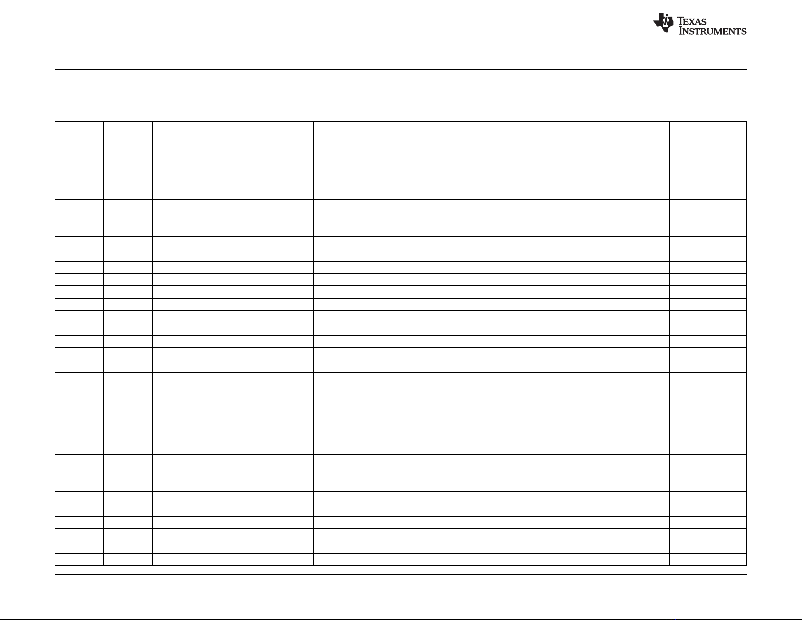
Table 2. Bill of Materials
-001 -002 RefDes Value Description Size Part Number MFR
bq24725A bq24735
1 1 C1 2.2 µF Capacitor, Ceramic, 25V, X7R, 10% 1210 Std Std
6 6 C2, C3, C4, C5, C6, C7 10 µF Capacitor, Ceramic, 25V, X7R, 10% 1206 Std Std
6 6 C8, C14, C15, C16, C17, 0.1 µF Capacitor, Ceramic, 25V, X7R, 10% 603 Std Std
C19
4 4 C9, C10, C20, C25 1 µF Capacitor, Ceramic, 25V, X7R, 10% 603 Std Std
3 3 C11, C12, C27 0.01 µF Capacitor, Ceramic, 25V, X7R, 10% 603 Std Std
0 0 C13, C18, C24 Open Capacitor, Ceramic, 25V, X7R, 10% 603 Std Std
1 1 C21 0.047 µF Capacitor, Ceramic, 25V, X7R, 10% 603 Std Std
1 1 C22 100 pF Capacitor, Ceramic, 25V, X7R, 10% 603 Std Std
1 1 C23 2200 pF Capacitor, Ceramic, 25V, X7R, 10% 603 Std Std
1 1 C26 1000 pF Capacitor, Ceramic, 25V, X7R, 10% 603 Std Std
1 1 D1 BAT54-V-G Diode, Schottky, 200-mA, 30-V SOT23 BAT54-V-G Vishay-Liteon
1 1 D2 BAT54C-V-G Diode, Dual Schottky, 200-mA, 30-V SOT23 BAT54C-V-G Vishay-Liteon
1 1 J1 ED120/2DS Terminal Block, 2-pin, 15-A, 5.1mm 0.40 x 0.35 inch ED120/2DS OST
1 1 J2 ED120/3DS Terminal Block, 3-pin, 15-A, 5.1mm 0.60 x 0.35 inch ED120/3DS OST
2 2 J3. J4 ED555/3DS Terminal Block, 3-pin, 6-A, 3.5mm 0.41 x 0.25 inch ED555/3DS OST
1 1 JP1 PEC02SAAN Header, Male 2-pin, 100mil spacing, 0.100 inch x 2 PEC02SAAN Sullins
1 1 SH1 929950-00 Shorting jumpers, 2-pin, 100mil spacing, 929950-00 3M/ESD
1 1 L1 4.7 µH Inductor, SMT 0.255 x 0.270 inch IHLP2525CZER4R7M01 Vishay
3 3 Q1, Q2, Q3 CSD17307Q5A MOSFET, NChan, 30V, 14A, 9.5millohm PWRPAK S0-8 CSD17307Q5A Texas Instruments
2 2 Q4, Q5 CSD17308Q3A MOSFET, NChan, 30V, 13A, 9.4millohm PWRPAK 1212 CSD17308Q3A Texas Instruments
1 1 Q6 BSS138W-7-F MOSFET, Nch, 50V, 200mA, SOT-323 BSS138W-7-F Diodes
2 2 R1, R2 0.01 Resistor, Chip, 1/2W, 1% 150PPM 1206 PMR18EZPFU10L0 Rohm
Resistor, Chip, 1W, 1% 75 PPM WSLP1206R0100FEA Vishay/Dale
1 1 R3 0 Resistor, Chip, 1/16W, 5% 603 Std Std
1 1 R5 20 Resistor, Chip, 1/16W, 1% 603 Std Std
1 1 R4 7.5 Resistor, Chip, 1/16W, 1% 603 Std Std
2 2 R6, R7 3.9 Resistor, Chip, 0.5W, 5% 1210 Std Std
3 3 R8, R9, R13 4.02k Resistor, Chip, 1/10W, 1% 603 Std Std
0 0 R10, R11 Open Resistor, Chip, 1/16W, 1% 603 Std Std
1 1 R12 1.00M Resistor, Chip, 1/16W, 1% 603 Std Std
1 1 R14 66.5k Resistor, Chip, 1/16W, 1% 603 Std Std
1 1 R15 430k Resistor, Chip, 1/16W, 1% 603 Std Std
1 1 R16 10.0 Resistor, Chip, 1/4W, 1% 1206 Std Std
3 3 R17, R18, R19 10.0k Resistor, Chip, 1/16W, 1% 603 Std Std
10 bq24735/725A Battery Charger Evaluation Module SLUU507A–June 2011–Revised September 2011
Submit Documentation Feedback
Copyright © 2011, Texas Instruments Incorporated