manuals.online logo
Brands
  1. Home
  2. •
  3. Brands
  4. •
  5. Texas Instruments
  6. •
  7. Batteries Charger
  8. •
  9. Texas Instruments BQ25157 User manual

Texas Instruments BQ25157 User manual

Other Texas Instruments Batteries Charger manuals

Texas Instruments BQ2463X EVM User manual

Texas Instruments

Texas Instruments BQ2463X EVM User manual

Texas Instruments BQ25123 User manual

Texas Instruments

Texas Instruments BQ25123 User manual

Texas Instruments BQ25120F3A User manual

Texas Instruments

Texas Instruments BQ25120F3A User manual

Texas Instruments BQ25120A User manual

Texas Instruments

Texas Instruments BQ25120A User manual

Texas Instruments bq24735 User manual

Texas Instruments

Texas Instruments bq24735 User manual

Texas Instruments BQ25155 User manual

Texas Instruments

Texas Instruments BQ25155 User manual

Texas Instruments bq2404 series User manual

Texas Instruments

Texas Instruments bq2404 series User manual

Texas Instruments SLUU477 User manual

Texas Instruments

Texas Instruments SLUU477 User manual

Texas Instruments bq24740/1EVM User manual

Texas Instruments

Texas Instruments bq24740/1EVM User manual

Texas Instruments bq2461 Series User manual

Texas Instruments

Texas Instruments bq2461 Series User manual

Texas Instruments bq2425xEVM-150 User manual

Texas Instruments

Texas Instruments bq2425xEVM-150 User manual

Popular Batteries Charger manuals by other brands

EVBox BusinessLine manual

EVBox

EVBox BusinessLine manual

Goobay 71808 user manual

Goobay

Goobay 71808 user manual

Kogan KACRDQIS4XA user manual

Kogan

Kogan KACRDQIS4XA user manual

Sealey WCB3 quick start guide

Sealey

Sealey WCB3 quick start guide

Vanner SP00143/181 owner's manual

Vanner

Vanner SP00143/181 owner's manual

KeyOuest KO037515 quick start guide

KeyOuest

KeyOuest KO037515 quick start guide

Enplus Silk Series user manual

Enplus

Enplus Silk Series user manual

Intermec SF51 user guide

Intermec

Intermec SF51 user guide

Colorovo PowerBox 6800 user guide

Colorovo

Colorovo PowerBox 6800 user guide

Smartech WBC-250 Operator's manual

Smartech

Smartech WBC-250 Operator's manual

PIXO C-USB instruction manual

PIXO

PIXO C-USB instruction manual

Gunson G4104 quick start guide

Gunson

Gunson G4104 quick start guide

Dometic NDS SCE320 Short Operating Manual

Dometic

Dometic NDS SCE320 Short Operating Manual

ABB HT572708 Operation manual

ABB

ABB HT572708 Operation manual

EVOline Square80 manual

EVOline

EVOline Square80 manual

Redarc SBC24025 Operating instructions and owner's manual

Redarc

Redarc SBC24025 Operating instructions and owner's manual

Absaar HV04 manual

Absaar

Absaar HV04 manual

DazeTechnology Cover Dazebox Home installation manual

DazeTechnology

DazeTechnology Cover Dazebox Home installation manual

manuals.online logo
manuals.online logoBrands
  • About & Mission
  • Contact us
  • Privacy Policy
  • Terms and Conditions

Copyright 2025 Manuals.Online. All Rights Reserved.

BQ25157 I2C Controlled 1-Cell 500-mA Linear Battery Charger With 10-nA Ship Mode,
Power Path With Regulated System (PMID) Voltage, ADC, LDO and 6.2-V OVP
1 Features
• Linear battery charger with 1.25-mA to 500-mA
fast charge current range
– 0.5% Accurate I2C programmable battery
regulation voltage ranging from 3.6 V to 4.6 V in
10-mV steps
– Configurable termination current supporting
down to 0.5 mA
– 20-V Tolerant input with typical 3.4-V to 6.2-V
input voltage operating range
– Programmable thermal charging profile, fully
configurable hot, warm, cool and cold
thresholds
• Power Path management for powering system and
charging battery
– Dynamic power path management optimizes
charging from weak adapters
– Advanced I2C control allows host to disconnect
the battery or adapter as needed
• I2C Configurable load switch or up to 150-mA LDO
output
– Programmable range from 0.6 V to 3.7 V in
100-mV steps
• Ultra low Iddq for extended battery life
– 10-nA Ship mode battery Iq
– 400-nA Iq While powering the system (PMID
and VDD on)
• One push-button wake-up and reset input with
adjustable timers
– Supports system power cycle and HW reset
• 16-Bit ADC
– Monitoring of charge current, battery thermistor
and battery, input and system (PMID) voltages
– General purpose ADC input
• Always on 1.8-V VDD LDO supporting loads up to
10 mA
• 20-Pin 2-mm x 1.6-mm CSP package
• 12-mm2 Total solution size
2 Applications
•Headsets, earbuds and hearing aids
•Smart watches and smart trackers
•Wearable fitness and activity monitors
•Blood glucose monitors
3 Description
The BQ25157 is a highly integrated battery charge
management IC that integrates the most common
functions for wearable, portable and small medical
devices, namely a charger, a regulated output voltage
rail for system power, ADC for battery and system
monitoring, a LDO, and push-button controller. The
BQ25157 has the Input Supply Over Voltage
Threshold (VOVP) threshold set to 6.2 V.
The BQ25157 IC integrates a linear charger with
Power Path that enables quick and accurate charging
for small batteries while providing a regulated voltage
to the system. The regulated system voltage (PMID)
output may be configured through I2C based on the
recommended operating condition of downstream IC's
and system loads for optimal system operation.
Device Information (1)
PART NUMBER PACKAGE BODY SIZE (NOM)
BQ25157 DSBGA (20) 2.00 mm x 1.60 mm
(1) For all available packages, see the orderable addendum at
the end of the data sheet.
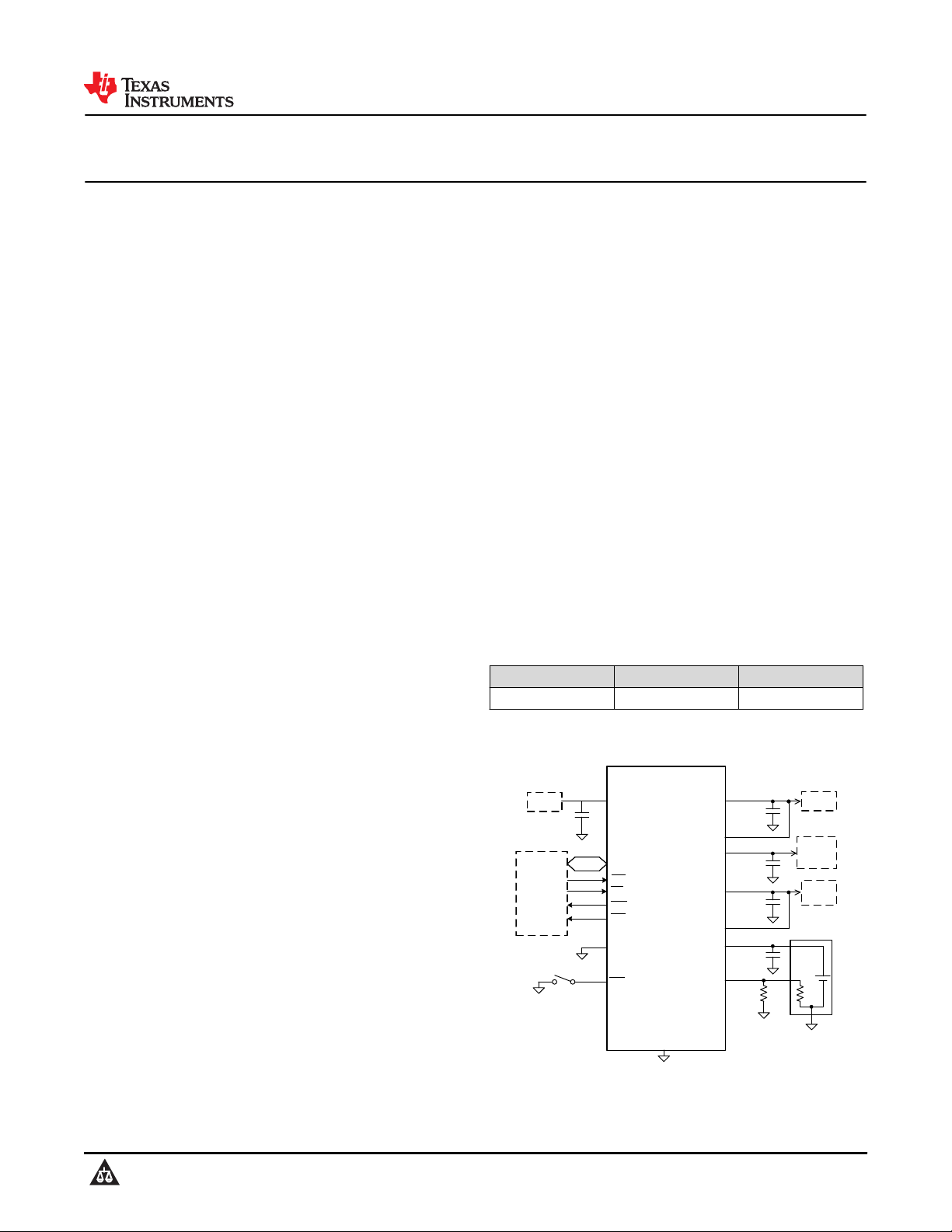
BQ25157
VINLS
PMID
LS/LDO
VDD
BAT
TS +
±
NTC
GND
IN
VIO
Host
USB
I2C Bus
<150mA
Load
<10mA
Load
System
ADCIN
MR
PG
INT
LP
CE
C4
C5
C3
C2
C1
Simplified Schematic
www.ti.com
BQ25157
SLUSEC5 – DECEMBER 2020
Copyright © 2020 Texas Instruments Incorporated Submit Document Feedback 1
Product Folder Links: BQ25157
BQ25157
SLUSEC5 – DECEMBER 2020
An IMPORTANT NOTICE at the end of this data sheet addresses availability, warranty, changes, use in safety-critical applications,
intellectual property matters and other important disclaimers. PRODUCTION DATA.
Table of Contents
1 Features............................................................................1
2 Applications..................................................................... 1
3 Description.......................................................................1
4 Revision History.............................................................. 2
5 Description (continued).................................................. 3
6 Device Key Default Settings........................................... 4
7 Pin Configuration and Functions...................................5
8 Specifications.................................................................. 7
8.1 Absolute Maximum Ratings........................................ 7
8.2 ESD Ratings............................................................... 7
8.3 Recommended Operating Conditions.........................7
8.4 Thermal Information....................................................7
8.5 Electrical Characteristics.............................................8
8.6 Timing Requirements................................................ 11
8.7 Typical Characteristics..............................................13
9 Detailed Description......................................................15
9.1 Overview................................................................... 15
9.2 Functional Block Diagram......................................... 15
9.3 Feature Description...................................................16
9.4 Device Functional Modes..........................................35
9.5 Register Map.............................................................39
10 Application and Implementation................................ 94
10.1 Application Information........................................... 94
10.2 Typical Application.................................................. 94
11 Power Supply Recommendations............................100
12 Layout.........................................................................101
12.1 Layout Guidelines................................................. 101
12.2 Layout Example.................................................... 101
13 Device and Documentation Support........................102
13.1 Device Support..................................................... 102
13.2 Documentation Support........................................ 102
13.3 Receiving Notification of Documentation Updates102
13.4 Support Resources............................................... 102
13.5 Electrostatic Discharge Caution............................102
13.6 Trademarks...........................................................102
13.7 Glossary................................................................102
14 Mechanical, Packaging, and Orderable
Information.................................................................. 103
4 Revision History
DATE REVISION NOTES
December 2020 * Initial release
BQ25157
SLUSEC5 – DECEMBER 2020 www.ti.com
2Submit Document Feedback Copyright © 2020 Texas Instruments Incorporated
Product Folder Links: BQ25157
5 Description (continued)
The device supports charge current up to 500 mA and supports termination current down to 0.5 mA for
maximum charge. The battery is charged using a standard Li-Ion charge profile with three phases: pre-charge,
constant current and constant voltage regulation.
The device integrates advanced power path management and control that allows the device to provide power to
the system while charging the battery even with poor adapters. The host may also control the power path
through I2C allowing it to disconnect the input adapter and/or battery without physically removing them. The
single push-button input eliminates the need of a separate button controller IC reducing the total solution
footprint. The push-button input can be used for wake functions or to reset the system.A 16-bit ADC enables
accurate battery voltage monitoring and can be used to enable a low Iq gauging to monitor battery health. It can
also be used to measure the battery temperature using a thermistor connected to the TS pin as well as external
system signals through the ADCIN pin. The low quiescent current during operation and shutdown enables
maximum battery life. The input current limit, charge current, LDO output voltage, and other parameters are
programmable through the I2C interface making the BQ25157 a very flexible charging solution. A voltage-based
JEITA compatible (or standard HOT/COLD) battery pack thermistor monitoring input (TS) is included that
monitors battery temperature and automatically changes charge parameters to prevent the battery from charging
outside of its safe temperature range. The temperature thresholds are also programable through I2C allowing the
host to customize the thermal charging profile. The charger is optimized for 5-V USB input, with 20-V absolute
maximum tolerance to withstand line transients. The device also integrates a linear regulator to provide a quiet
rail for radios or processors and can be independently sourced and controlled through I2C.
www.ti.com
BQ25157
SLUSEC5 – DECEMBER 2020
Copyright © 2020 Texas Instruments Incorporated Submit Document Feedback 3
Product Folder Links: BQ25157
6 Device Key Default Settings
PARAMETER BQ25150 BQ25155 BQ25157
Fast Charge Current (ICHARGE) 10 mA 10 mA 10 mA
Pre-Charge Current (IPRECHARGE) 2.5 mA 2.5 mA 2.5 mA
OVP 5.5V 5.5 V 6.2V
Default Input Current Ljmit (IILIM) 100 mA 500 mA 100 mA
VIN DPM Enabled (4.5 V) Disabled (4.6 V) Enabled (4.2 V)
PMID Passthrough Regulated (4.5V Default) Passthrough
IMAX Enabled Disabled Disabled
Ship Mode Wake Timer 2 seconds 0.125 seconds 2 seconds
DEVICE_ID 0x20h 0x35h 0x3Ch
BQ25157
SLUSEC5 – DECEMBER 2020 www.ti.com
4Submit Document Feedback Copyright © 2020 Texas Instruments Incorporated
Product Folder Links: BQ25157
7 Pin Configuration and Functions
IN PMID BAT GND
/PG PMID BAT TS
/MR /CE NC ADCIN
VDD /INT /LP LSLDO
VIO SDA SCL VINLS
A
B
C
D
E
1 2 3 4
Figure 7-1. YFP Package 20-Pin DSBGA Top View
Table 7-1. Pin Functions
PIN I/O DESCRIPTION
NAME NO.
IN A1 I DC Input Power Supply. IN is connected to the external DC supply. Bypass IN to GND with
at least 1-µF of capacitance using a ceramic capacitor.
PMID A2, B2 I/O
Regulated System Output. Connect 10-µF capacitor from PMID to GND as close to the
PMID and GND pins as possible. (at least 3-µF of ceramic capacitance with DC bias de-
rating). Note: Shorting PMID to IN pin is not recommended as it may cause large discharge
current from battery to IN if IN pin is not truly floating.
GND A4 PWR Ground connection. Connect to the ground plane of the circuit.
VDD D1 O Digital supply LDO. Connect a 2.2-µF from this pin to ground. A 4.7-µF capacitor to ground
recommended if loaded externally.
CE C2 I
Charge Enable. Drive CE low or leave disconnected to enable charging when VIN is valid.
Drive CE high to disable charge when VIN is present. CE is pulled low internally with 900-kΩ
resistor. CE has no effect when VIN is not present.
SCL E3 I/O I2C Interface Clock. Connect SCL to the logic rail through a 10-kΩ resistor.
SDA E2 I I2C Interface Data. Connect SDA to the logic rail through a 10-kΩ resistor.
LP D3 I
Low Power Mode Enable. Drive this pin low to set the device in low power mode when
powered by the battery. This pin must be driven high to allow I2C communication when VIN
is not present. LP is pulled low internally with 900-kΩ resistor. This pin has no effect when
VIN is present.
ADCIN C4 I Input Channel to the ADC. Maximum ADC range 1.2 V. If not used it may be left floating or
connect to ground.
MR C1 I
Manual Reset Input. MR is a general purpose input that must be held low for greater than
tHWRESET to go into HW Reset and power cycle the output rails. If MR is also used to wake
up the device out of Ship Mode when pressed for at least tWAKE1. MR has in internal 125-kΩ
pull-up resistor to BAT.
www.ti.com
BQ25157
SLUSEC5 – DECEMBER 2020
Copyright © 2020 Texas Instruments Incorporated Submit Document Feedback 5
Product Folder Links: BQ25157
Table 7-1. Pin Functions (continued)
PIN I/O DESCRIPTION
NAME NO.
LS/LDO D4 O
Load Switch or LDO output. Connect 2.2 µF of ceramic capacitance to this pin to assure
stability. Be sure to account for capacitance bias voltage derating when selecting the
capacitor. If LDO is not used, short to VINLS
VINLS E4 I Input to the Load Switch / LDO output. Connect at least 1 µF of ceramic capacitance from
this pin to ground.
BAT A3, B3 I/O Battery Connection. Connect to the positive terminal of the battery. Bypass BAT to GND with
at least 1 µF of ceramic capacitance.
TS B4 I Battery Pack NTC Monitor. Connect TS to a 10-kΩ NTC thermistor in parallel to a 10-kΩ
resistor. If TS function is not to be used connect a 5-kΩ resistor from TS to ground.
PG B1 O
Open-drain Power Good status indication output. PG is pulled to GND when VIN is above
VBAT+ VSLP and less than VOVP. PG is high-impedance when the input power is not within
specified limits. Connect PG to the desired logic voltage rail using a 1-kΩ to 100-kΩ resistor,
or use with an LED for visual indication. PG can also be configured through I2C as a push-
button level shifted output ( MR), where the output of the PG pin reflects the status of the
MR input, but pulled up to the desired logic voltage rail using a 1-kΩ to 100-kΩ resistor. The
PG pin can also be configured as a general purpose open drain output.
VIO E1 I
System IO supply. Connect to system IO supply to allow level shifting of input signals (SDA,
SCL, LP and CE) to the device internal digital domain. Connect to VDD when external IO
supply is not available.
NC C3 I No Connect. Connect to ground if possible for better thermal dissipation or leave floating. Do
not connect to a any voltage source or signal to avoid higher quiescent current.
BQ25157
SLUSEC5 – DECEMBER 2020 www.ti.com
6Submit Document Feedback Copyright © 2020 Texas Instruments Incorporated
Product Folder Links: BQ25157
8 Specifications
8.1 Absolute Maximum Ratings
over operating free-air temperature range (unless otherwise noted)(1)
MIN MAX UNIT
Voltage
IN –0.3 20 V
TS, ADCIN, VDD, NC –0.3 1.95 V
VINLS, PMID -0.3 6.2 V
All other pins –0.3 5.5 V
Current
IN 0 800 mA
BAT, PMID –0.5 1.5 A
INT, ADCIN, PG 0 10 mA
Junction temperature, TJ–40 125 °C
Storage temperature, Tstg –55 150 °C
(1) Stresses beyond those listed under Absolute Maximum Rating may cause permanent damage to the device. These are stress ratings
only, which do not imply functional operation of the device at these or any other conditions beyond those indicated under
Recommended Operating Condition. Exposure to absolute-maximum-rated conditions for extended periods may affect device
reliability.
8.2 ESD Ratings
VALUE UNIT
V(ESD) Electrostatic discharge
Human body model (HBM), per ANSI/ESDA/
JEDEC JS-001, all pins(1) ±2000
V
Charged device model (CDM), per JEDEC
specification JESD22-C101, all pins(2) ±500
(1) JEDEC document JEP155 states that 500-V HBM allows safe manufacturing with a standard ESD control process.
(2) JEDEC document JEP157 states that 250-V CDM allows safe manufacturing with a standard ESD control process.
8.3 Recommended Operating Conditions
over operating free-air temperature range (unless otherwise noted)
MIN NOM MAX UNIT
VBAT Battery voltage range 2.4 4.6 V
VIN Input voltage range 3.15 6.05
(1) V
VINLS LDO input voltage range 2.2 6.05(1) V
VIO IO supply voltage range 1.2 3.6 V
VADCIN ADC input voltage range 0 1.2 V
ILDO LDO output current 0 100 mA
IPMID PMID output current 0 1.5 A
TAOperating free-air temperature range –40 85 °C
(1) Based on minimum VOVP value. 6.2V under typical conditions
8.4 Thermal Information
THERMAL METRIC(1)
BQ25157
UNITYFP (DSBGA)
20-PIN
RθJA Junction-to-ambient thermal resistance (2) 36.1 °C/W
RθJA Junction-to-ambient thermal resistance 74.4 °C/W
RθJC(top) Junction-to-case (top) thermal resistance 0.5 °C/W
www.ti.com
BQ25157
SLUSEC5 – DECEMBER 2020
Copyright © 2020 Texas Instruments Incorporated Submit Document Feedback 7
Product Folder Links: BQ25157
8.4 Thermal Information (continued)
THERMAL METRIC(1)
BQ25157
UNITYFP (DSBGA)
20-PIN
RθJB Junction-to-board thermal resistance 17.6 °C/W
ΨJT Junction-to-top characterization parameter 0.3 °C/W
ΨJB Junction-to-board characterization parameter 17.7 °C/W
RθJC(bot) Junction-to-case (bottom) thermal resistance N/A °C/W
(1) For more information about traditional and new thermal metrics, see the Semiconductor and IC Package Thermal Metrics application
report.
(2) Measured in BQ25157EVM board.
8.5 Electrical Characteristics
VIN = 5V, VBAT = 3.6V. -40°C < TJ < 125°C unless otherwise noted. Typical data at TJ = 25°C
PARAMETER TEST CONDITIONS MIN TYP MAX UNIT
INPUT CURRENTS
IIN Input supply current
PMID_MODE = 01, VIN = 5V, VBAT = 3.6V 500 µA
0°C <TJ < 85°C , VIN = 5V, VBAT = 3.6V
Charge Disabled 2 mA
IBAT_SHIP Battery Discharge Current in Ship Mode 0°C <TJ < 60°C ,VIN = 0V , VBAT = 3.6V 10 150 nA
IBAT_LP
Battery Quiescent Current in Low-power
Mode
0°C <TJ < 60°C ,VIN = 0V , VBAT = 3.6V,
LDO Disabled 0.46 1.2 µA
0°C <TJ < 60°C ,VIN = 0V , VBAT = 3.6V,
LDO Enabled 1.7 3.5 µA
IBAT_ACTI
VE
Battery Quiescent Current in Active Mode
0°C <TJ < 85°C ,VIN = 0V , VBAT = 3.6V,
LDO Disabled 18 25 µA
0°C <TJ < 85°C ,VIN = 0V , VBAT = 3.6V,
LDO Enabled 21 27 µA
POWER PATH MANAGEMENT AND INPUT CURRENT LIMIT
RON(IN-
PMID)
Input FET ON resistance IILIM = 500mA (ILIM = 110), VIN = 5V, IIN =
150mA 280 520 mΩ
VBSUP1 Enter supplements mode threshold VBAT > VBATUVLO, DPPM enabled or
Charge disabled
VPMID <
VBAT –
40mV
mV
VBSUP2 Exit supplements mode threshold VBAT > VBATUVLO, DPPM enabled or
Charge disabled
VPMID <
VBAT –
20mV
mV
IILIM Input Current Limit
Programmable Range 50 600 mA
IILIM = 50mA 45 50 mA
IILIM = 100mA 90 100 mA
IILIM = 150mA 135 150 mA
IILIM = 500mA 450 500 mA
VIN_DPM
Input DPM voltage threshold where
current in reduced Programmable Range 4.2 4.9 V
Accuracy –3 3 %
BATTERY CHARGER
VDPPM
PMID voltage threshold when charge
current is reduced VPMID - VBAT 200 mV
RON(BAT-
PMID)
Battery Discharge FET On Resistance VBAT = 4.35V, IBAT = 100mA 100 135 mΩ
VBATREG
Charge Voltage Programmable charge voltage range 3.6 4.6 V
Voltage Regulation Accuracy 0.5 0.5 %
BQ25157
SLUSEC5 – DECEMBER 2020 www.ti.com
8Submit Document Feedback Copyright © 2020 Texas Instruments Incorporated
Product Folder Links: BQ25157
8.5 Electrical Characteristics (continued)
VIN = 5V, VBAT = 3.6V. -40°C < TJ < 125°C unless otherwise noted. Typical data at TJ = 25°C
PARAMETER TEST CONDITIONS MIN TYP MAX UNIT
ICHARGE
Fast Charge Programmable Current
Range VLOWV < VBAT < VBATREG 1.25 500 mA
Fast Charge Current Accuracy TJ = 25°C, ICHARGE > 5mA –5 5 %
IPRECHAR
GE
Precharge current Precharge current programmable range 1.25 77.5 mA
Precharge Current Accuracy -40°C < TJ < 85°C –10 10 %
ITERM
Termination Charge Current Termination Current Programmable
Range 1 31 %
Accuracy
TJ = 25°C, ITERM = 10% ICHARGE, ICHARGE
= 100mA –5 5 %
-10°C < TJ < 85°C, ITERM = 10% ICHARGE,
ICHARGE = 100mA –10 10 %
VLOWV
Programmable voltage threshold for pre-
charge to fast charge transitions VBAT rising. Programmable Range 2.8 3 V
VSHORT
Battery voltage threshold for short
detection VBAT falling, VIN = 5V 2.41 2.54 2.67 V
ISHORT Charge Current in Battery Short Condition VBAT < VSHORT
IPRECHAR
GE
mA
VRCH Recharge Threshold voltage
VBAT falling, VBATREG = 4.2V, VRCH =
140mV setting 140 mV
VBAT falling, VBATREG = 4.2V, VRCH =
200mV setting 200 mV
RPMID_PD PMID pull-down resistance VPMID = 3.6V 25 Ω
VDD
VDD VDD LDO output voltage VBAT = 3.6V, VIN = 0V, 0 < ILOAD_VDD <
10mA 1.8 V
ILOAD_VD
D
Maximum VDD External load capability VPMID > 3V 10 mA
LS/LDO
VINLS
Input voltage range for Load switch Mode 0.8 6.2 V
Input voltage range for LDO Mode
2.2 or
VLDO +
500mV
6.2 V
VLDO
LDO programmable output voltage range 0.6 3.7 V
LDO output accuracy TJ = 25°C –2 2 %
VLDO = 1.8V, VINLS =3.6V. ILOAD = 1mA –3 3 %
ΔVOUT/
ΔIOUT
DC Load Regulation 0°C < TJ < 85°C, 1 mA < IOUT < 150mA,
VLDO = 1.8V 1.2 %
ΔVOUT/
ΔVIN
DC Line Regulation 0°C < TJ < 85°C, Over VINLS range, IOUT =
100mA, VLDO = 1.8V 0.5 %
RDOSN_LD
O
Switch On resistance VINLS = 3.6V 250 450 mΩ
RDSCH_LS
LDO
Discharge FET On-resistance for LS VINLS = 3.6V 40 Ω
IOCL_LDO Output Current Limit VLS/LDO = 0V 200 300 mA
IIN_LDO
LDO VINLS quiescent current in LDO
mode VBAT = VINLS=3.6V 0.9 µA
OFF State Supply Current VBAT = VINLS=3.6V 0.25 µA
ADC
Resolutio
nBits reported by ADC 16 Bits
www.ti.com
BQ25157
SLUSEC5 – DECEMBER 2020
Copyright © 2020 Texas Instruments Incorporated Submit Document Feedback 9
Product Folder Links: BQ25157
8.5 Electrical Characteristics (continued)
VIN = 5V, VBAT = 3.6V. -40°C < TJ < 125°C unless otherwise noted. Typical data at TJ = 25°C
PARAMETER TEST CONDITIONS MIN TYP MAX UNIT
tADC_CON
V
Conversion-time
ADC_SPEED = 00 24 ms
ADC_SPEED = 01 12 ms
ADC_SPEED = 10 6 ms
ADC_SPEED = 11 3 ms
Resolutio
nEffective Resolution ADC_SPEED = 00 12 Bits
ADC_SPEED = 10 10 Bits
Accuracy
ADC TS Accuracy ADC_SPEED = 00, VTS = 0.4V, -10°C <
TJ < 85°C –1 1 %
ADC ADCIN Accuracy ADC_SPEED = 00, VADCIN = 0.4V, -10°C
< TJ < 85°C –1 1 %
ADC VBAT Accuracy ADC_SPEED = 00, VBAT = 4.2V, -10°C <
TJ < 85°C –0.4 0.4 %
BATTERY PACK NTC MONITOR
VHOT High temperature threshold VTS falling, -10°C < TJ < 85°C 0.182 0.185 0.189 V
VWARM Warm temperature threshold VTS falling, -10°C < TJ < 85°C 0.262 0.265 0.268 V
VCOOL Cool temperature threshold VTS rising, -10°C < TJ < 85°C 0.510 0.514 0.518 V
VCOLD Cold temperature threshold VTS rising, -10°C < TJ < 85°C 0.581 0.585 0.589 V
VOPEN TS Open threshold VTS rising, -10°C < TJ < 85°C 0.9 V
VHYS Threshold hysteresis 4.7 mV
ITS_BIAS TS bias current -10°C < TJ < 85°C 78.4 80 81.6 µA
PROTECTION
VUVLO IN active threshold voltage VIN rising 3.4 V
VIN falling 3.25 V
VBATUVLO
Battery undervoltage Lockout Threshold
Voltage Programmable range, 150 mV Hysteresis 2.4 3 V
Accuracy –3 3 %
Battery undervoltage Lockout Threshold
Voltage at Power Up VBAT rising, VIN = 0V, TJ = 25°C 3.15 V
VSLP_ENT
RY
Sleep Entry Threshold (VIN - VBAT) 2.0V < VBAT < VBATREG, VIN falling 80 mV
VSLP_EXIT Sleep Exit Threshold (VIN - VBAT) 2.0V < VBAT < VBATREG 130 mV
VOVP Input Supply Over Voltage Threshold VIN rising 6.05 6.2 6.5 V
VIN falling (125mV hysteresis) 6.1 V
IBAT_OCP
Battery Over Current Threshold
Programmable range IBAT_OCP increasing 1200 1600 mA
Current Limit Accuracy –30 30 %
TSHUTDO
WN
Thermal shutdown trip point 125 °C
THYS Thermal shutdown trip point hysteresis 15 °C
I2C INTERFACE (SCL and SDA)
I2C Frequency 100 400 kHz
VIL Input Low threshold level VPULLUP = VIO = 1.8V 0.25 *
VIO
V
VIH Input High Threshold level VPULLUP = VIO = 1.8V 0.75 *
VIO
V
VOL Output Low threshold level VPULLUP = VIO = 1.8V, ILOAD = 5mA 0.25 *
VIO
V
ILKG High-level leakage Current VPULLUP = VIO = 1.8V 1 µA
BQ25157
SLUSEC5 – DECEMBER 2020 www.ti.com
10 Submit Document Feedback Copyright © 2020 Texas Instruments Incorporated
Product Folder Links: BQ25157