www.ti.com
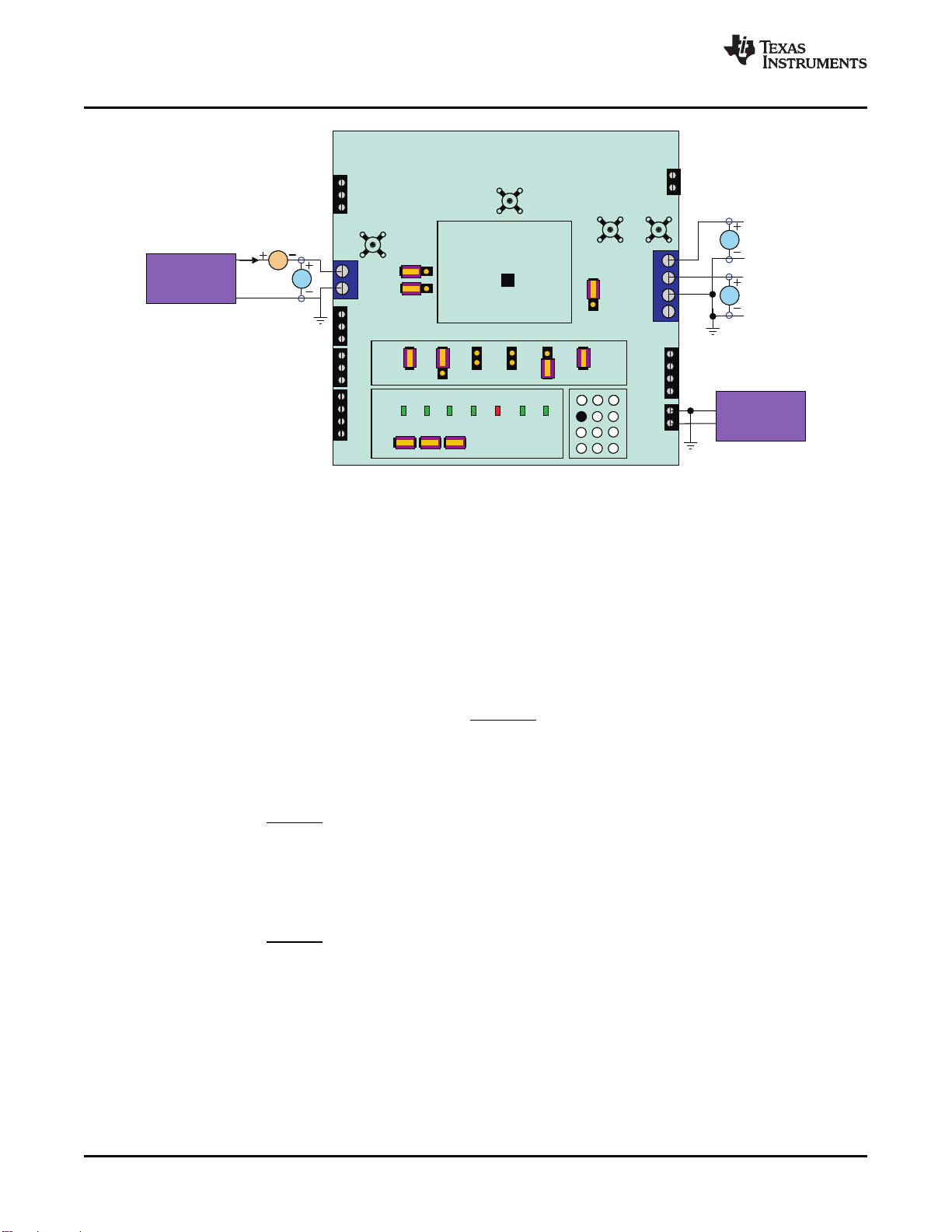
Bill of Materials, Board Layout, and Schematics
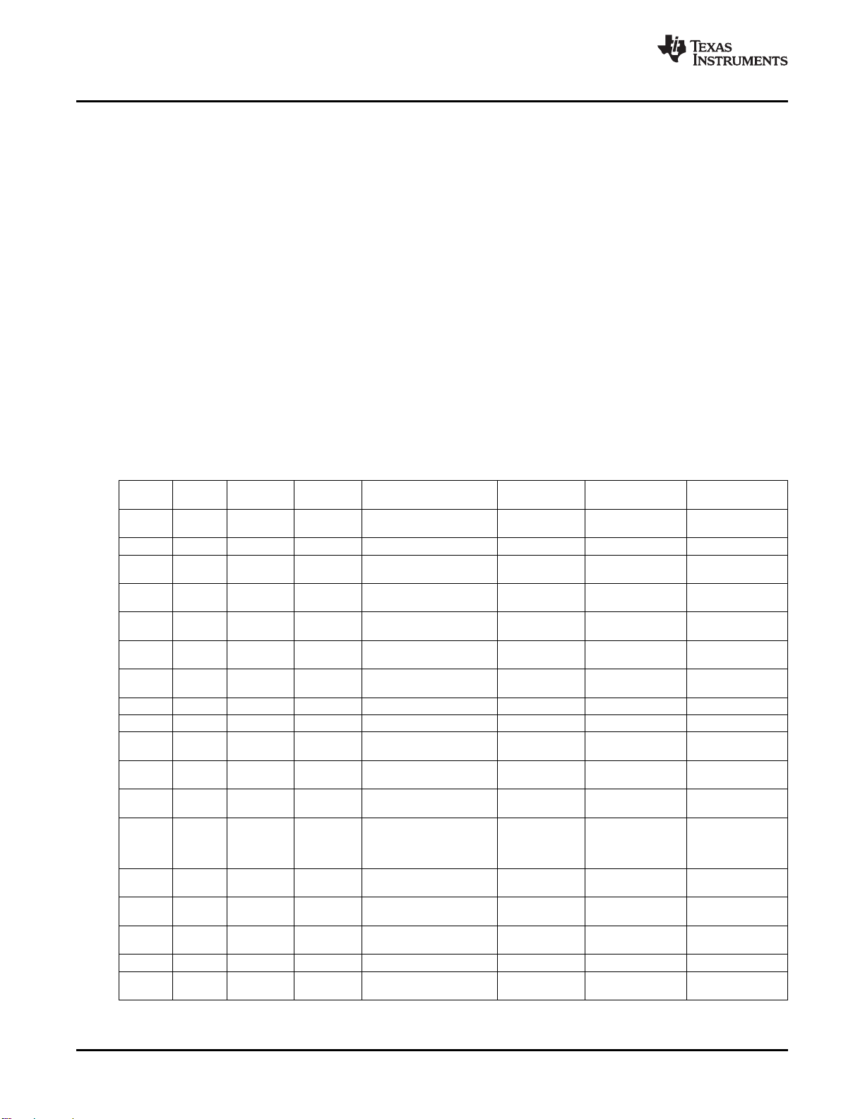
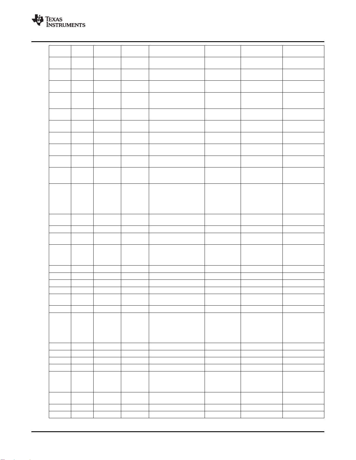
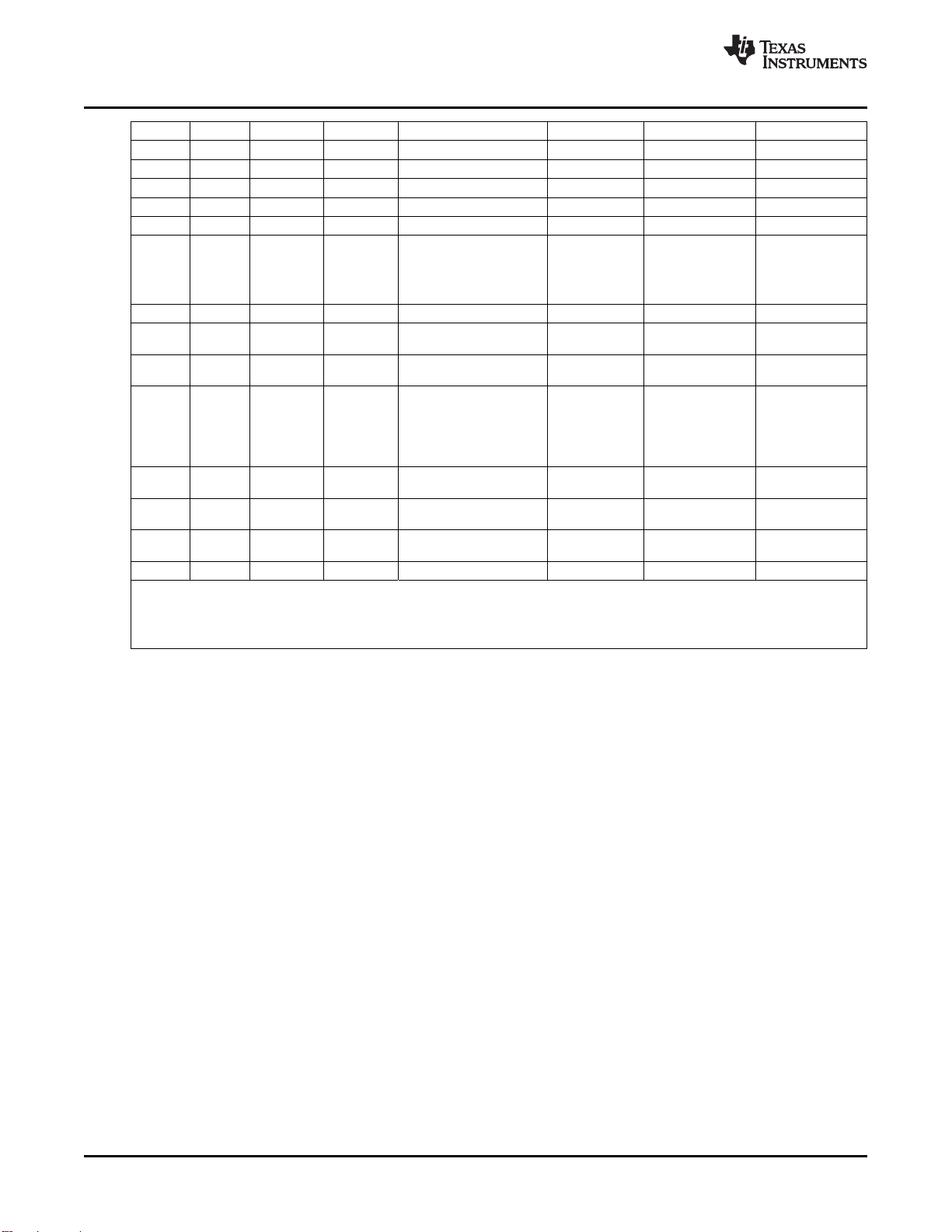
2 2 J10, J16 ED555/2DS Terminal Block, 2-pin, 6-A, 0.27 x 0.25 inch ED555/2DS OST3.5mm
5 5 J2, J3, J5, PTC36SAAN Header, 3-pin, 100mil 0.100 inch x 3 PTC36SAAN SullinsJ13, J21 spacing, (36-pin strip)
3 3 J4, J11, J12 ED555/3DS Terminal Block, 3-pin, 6-A, 0.41 x 0.25 inch ED555/3DS OST3.5mm
2 2 J6, J14 ED555/4DS Terminal Block, 4-pin, 6-A, 0.55 x 0.25 inch ED555/4DS OST3.5mm
7 7 J7, J9, J15, PTC36SAAN Header, 2-pin, 100mil 0.100 inch x 2 PTC36SAAN SullinsJ17, J18, spacing, (36-pin strip)J19, J20
1 1 J8 D120/4DS Terminal Block, 4-pin, 15-A, 0.80 x 0.35 inch D120/4DS OST5.1mm
1 0 L1 8.2uH Inductor, SMT, 16A, 0.51 x 0.51 inch IHLP5050CE8R2M0 Vishay24.8milliohm 1
0 1 L1 10uH Inductor, SMT, 16A, 0.51 x 0.51 inch IHLP5050CE10RM0 Vishay24.8milliohm 1
3 3 Q1, Q2, Q3 Si4435DY MOSFET, P-ch, 30-V, 8.0-A, SO8 Si4435DY Siliconix20-milliohm
3 3 Q12, Q14, TP0610K Mosfet, P-Ch, 60V, Rds 6 SOT-23 TP0610K Vishay-SiliconixQ16 ohms, Id 185 mA
2 2 Q4, Q5 FDS6680A Transistor, MOSFET, SO8 FDS6680A FairchildNChan, 30V, 12.5A, Rds 9.5milliohm
12 12 Q6, Q7, 2N7002DICT MOSFET, N-ch, 60-V, SOT23 2N7002DICT Vishay-LiteonQ10, Q13, 115-mA, 1.2-OhmsQ15, Q17,Q18, Q19,Q20, Q21,Q22, Q23
3 3 Q8, Q9, Q11 NDS0605 MOSFET,P-ch, -60 V, SOT-23 NDS0605 Vishay180-mA, 5 Ohms
1 1 R1 430K Resistor, Chip, 1/16W, 1% 0603 STD STD
2 2 R10, R50 4 Anti-surge Resistor, Chip, 1210 ERJ-P14J4R0U Panasonic - ECG1/2W, 5%
8 8 R11, R3, R4, 10K Resistor, Chip, 1/16W, 1% 0402 STD STDR18, R19,R22, R44,R48
1 1 R12 0.01 Resistor, Chip, 1/2W, 1% 2010 STD STD
1 0 R13 0.01 Resistor, Chip, 1/2W, 1% 2010 STD STD
0 1 R13 0.02 Resistor, Chip, 1/2W, 1% 2010 STD STD
2 2 R14, R15 10K Resistor, Chip, 1/16W, 5% 0603 STD STD
3 3 R16, R45, 100K Resistor, Chip, 1/10W, 0.1% 0805 STD STDR49
1 1 R2 66.5K Resistor, Chip, 1/16W, 1% 0603 STD STD
12 12 R20, R5, 100K Resistor, Chip, 1/16W, 5% 0402 STD STDR17, R21,R23, R26,R28, R29,R31, R32,R34, R35
1 1 R24 68K Resistor, Chip, 1/10W, 0.1% 0805 STD STD
2 2 R25, R43 0 ohm Resistor, Chip, 1/16W, 5% 0402 STD STD
1 0 R27 43K Resistor, Chip, 1/10W, 0.1% 0805 STD STD
0 1 R27 150K Resistor, Chip, 1/10W, 0.1% 0805 STD STD
7 7 R30, R33, 2.2K Resistor, Chip, 1/16W, 5% 0603 STD STDR36, R38,R39, R41,R42
3 3 R37, R40, 20K Resistor, Chip, 1/16W, 5% 0603 STD STDR47
1 0 R46 82K Resistor, Chip, 1/10W, 0.1% 0805 STD STD
0 1 R46 66.5K Resistor, Chip, 1/10W, 0.1% 0805 STD STD
SLUU284A – June 2007 – Revised October 2008 bq24740/1EVM (HPA206) For Multicell Synchronous Notebook Charger 9Submit Documentation Feedback