Texas Instruments bq2425xEVM-150 User manual

User's Guide
SLUUA08A–March 2013–Revised April 2013
bq2425xEVM-150, Single-Cell Li-Ion Switch-Mode Charger
This user's guide describes the characteristics, operation, and use of the bq24250EVM-150,
bq24251EVM-150, and bq24257EVM-150 evaluation modules (EVM). These EVMs enable test and
evaluation TI's bq24250, bq24251, and bq24257 devices. The bq2425x series are highly integrated,
single-cell, Li-Ion battery chargers targeted for space-limited, portable applications with high-capacity
batteries. This user's guide includes EVM specifications, the schematic diagram, test procedures, test
results, a bill of materials, and board layout.
Contents
1 Introduction .................................................................................................................. 2
2 EVM Considerations ........................................................................................................ 3
3 Recommended Operating Condition ..................................................................................... 3
4 Equipment and EVM Setup ................................................................................................ 4
4.1 Schematic ........................................................................................................... 4
4.2 I/O Description ...................................................................................................... 5
4.3 Test Points .......................................................................................................... 5
4.4 Pin Descriptions .................................................................................................... 6
4.5 Control and Key Parameters Setting ............................................................................ 6
5 Test Procedure .............................................................................................................. 7
5.1 Definition ............................................................................................................ 7
5.2 Recommended Test Equipment ................................................................................. 7
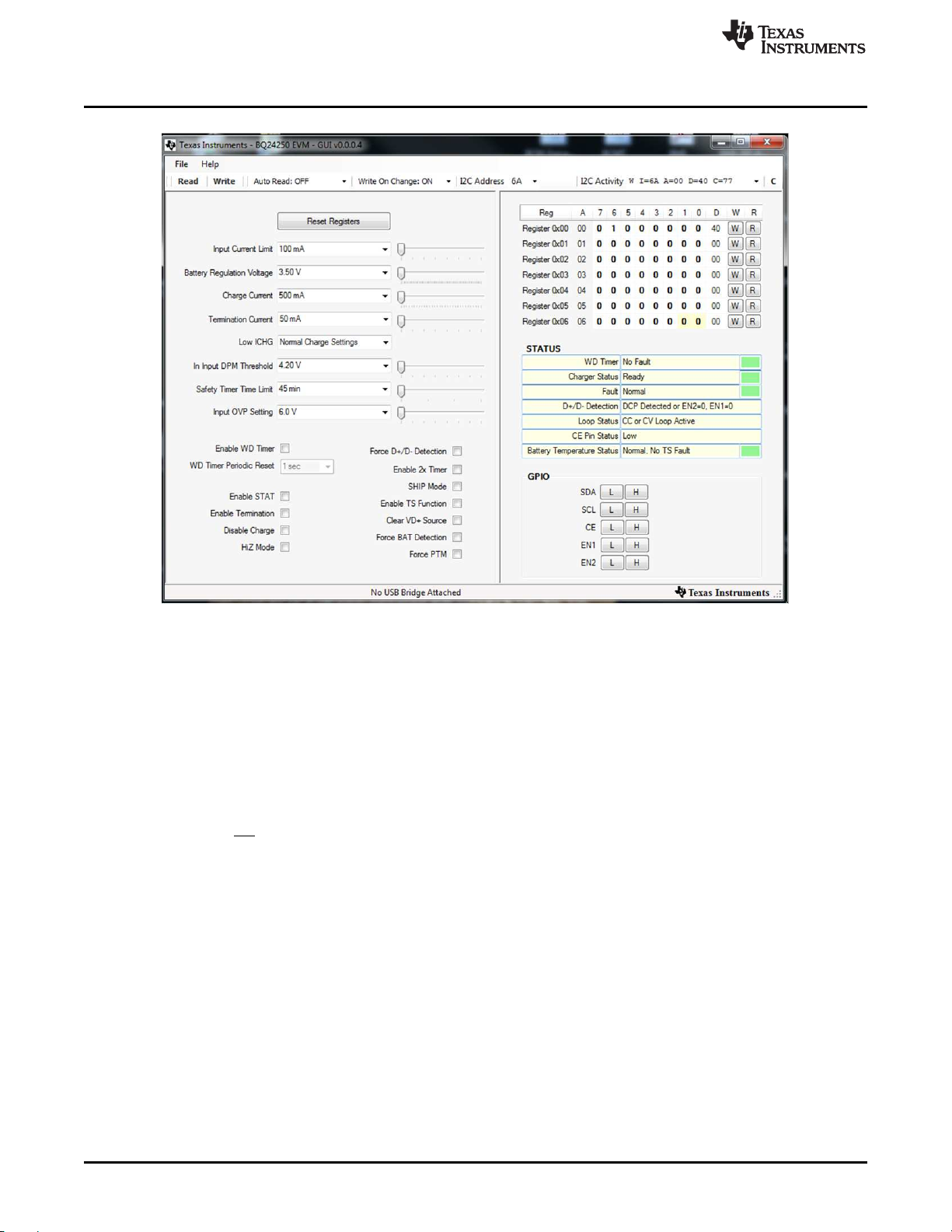
5.3 Software ............................................................................................................. 7
5.4 Recommended Test Equipment Set Up ........................................................................ 8
5.5 Recommended Test Procedure ................................................................................ 10
6 Test Results ................................................................................................................ 12
6.1 Output Regulation Ripple ........................................................................................ 12
6.2 Efficiency Data .................................................................................................... 12
6.3 Thermal Performance ............................................................................................ 13
7 Layout and Bill of Materials .............................................................................................. 13
7.1 Printed-Circuit Board Layout Guideline ........................................................................ 13
7.2 Layout .............................................................................................................. 14
7.3 Bill of Materials (BOM) ........................................................................................... 20
List of Figures
1 bq2425xEVM-150 Schematic ............................................................................................. 4
2 Original Test Setup ......................................................................................................... 8
3 Battery Emulator ........................................................................................................... 9
4 Connector Kit................................................................................................................ 9
5 Main Window of the bq2425xSW Evaluation Software............................................................... 10
6 Output Regulation Ripple at ICHG = 1000 mA ....................................................................... 12
7 Output Regulation Ripple at ICHG = 120 mA ......................................................................... 12
8 Efficiency Versus Output Current While in Battery Voltage Regulation (4.2V)”................................... 12
9 Thermal Image............................................................................................................. 13
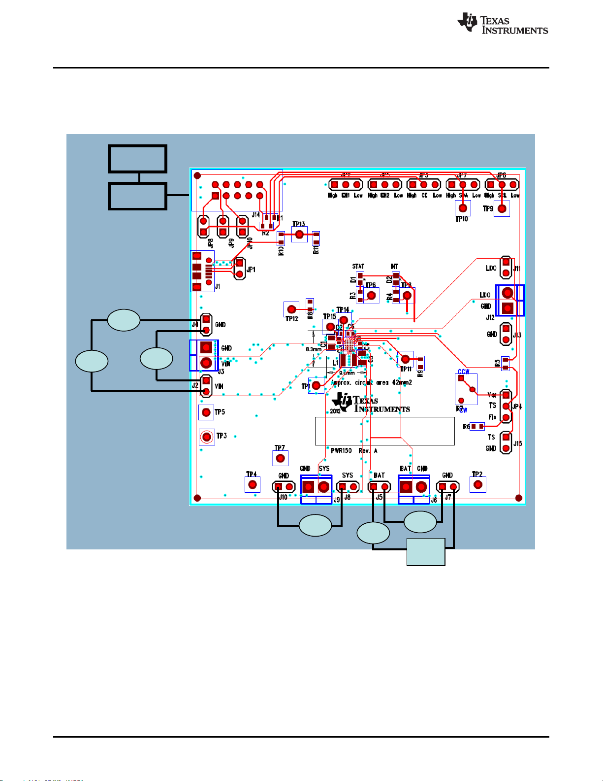
10 bq2425xEVM-150 Top Assembly ....................................................................................... 14
11 bq2425xEVM-150 Top Silkscreen ...................................................................................... 15
I2C is a trademark of NXP.
1
SLUUA08A–March 2013–Revised April 2013 bq2425xEVM-150, Single-Cell Li-Ion Switch-Mode Charger
Submit Documentation Feedback Copyright © 2013, Texas Instruments Incorporated

Introduction
www.ti.com
12 bq2425xEVM-150 Top Layer ............................................................................................ 16
13 bq2425xEVM-150 Second Layer (Internal) Routine .................................................................. 17
14 bq2425xEVM-150 Third Layer (Internal) Routine .................................................................... 18
15 bq2425xEVM-150 Bottom Layer ........................................................................................ 19
List of Tables
1 Connector and Test Points ................................................................................................ 5
2 Test Points Description..................................................................................................... 5
3 Pin Descriptions............................................................................................................. 6
4 Control and Key Parameters .............................................................................................. 6
5 bq2425xEVM-150 Bill of Materials ..................................................................................... 20
1 Introduction
The bq24250, bq24251, and bq24257 devices are highly-integrated, single-cell, Li-Ion battery chargers
with integrated current sense resistors targeted for space-limited, portable applications with high-capacity
batteries. The single-cell charger has a single input that operates from either a USB port or AC wall
adapter for a versatile solution. BC1.2-compliant D+/D– detection allows for recognition of CDP, DCP,
SDP, and non-standard USB adapters. The use of an accessory dead-battery provision (DBP) pin allows
for the system to sync a dead battery state in order to enable/disable the BC1.2 detection in the case of
an external USB-PHI.
The bq24250, bq24251, and bq24257 devices have two modes of operation: 1) I2C™ mode, and 2)
standalone mode. In I2C mode, the host adjusts the charge parameters and monitors the status of the
charger operation. In standalone mode, the external resistor sets the input-current limit, and charge-
current limit. Standalone mode also serves as the default settings when a DCP adapter is present. They
enter host mode while the I2C registers are accessed and the watchdog timer has not expired (if enabled).
The battery is charged in four phases: trickle charge, pre-charge, constant current and constant voltage. In
all charge phases, an internal control loop monitors the IC junction temperature and reduces the charge
current if the internal temperature threshold is exceeded.
The bq24250 and bq24251 have system power path management. This feature allows this device to
power the system from a high efficiency DC/DC converter while simultaneously and independently
charging the battery. The charger monitors the battery current at all times and reduces the charge current
when the system load requires current above the input current limit. This allows for proper charge
termination and enables the system to run with a defective or absent battery pack. Additionally, this
enables instant system turn-on even with a totally discharged battery or no battery. The power-path
management architecture also permits the battery to supplement the system current requirements when
the adapter cannot deliver the peak system currents. This enables the use of a smaller adapter.
2bq2425xEVM-150, Single-Cell Li-Ion Switch-Mode Charger SLUUA08A–March 2013–Revised April 2013
Submit Documentation Feedback
Copyright © 2013, Texas Instruments Incorporated

www.ti.com
EVM Considerations
2 EVM Considerations
Refer to the data sheet for specific details on the charger ICs. The bq24250, bq24251, and bq24257
devices are featured with a high-efficiency switch-mode charger. It has integrated power FETs able to
charge at up to a 2-A charging rate, and an integrated 50-mA LDO. In I2C mode, the bq24250, bq24251,
and bq24257 devices have programmable battery charge voltage (VBATREG), charge current (ICHG), input
current limit (ILIM), and input over-voltage protection threshold (VOVP).
The charge current and the input current limit are programmed using external resistors (RISET and RILIM)
connected from the ISET and ILIM pins to ground. The range of these resistors can be found in the
datasheet. Both of these currents can be programmed up to 2 A. The bq24250, bq24251, and bq24257
devices also have complete system-level protection such as input undervoltage lockout (UVLO), input
over-voltage protection (OVP), battery OVP, sleep mode, thermal regulation and thermal shutdown,
voltage-based JEITA-compatible NTC monitoring input, and safety timer. PSE is also available – notify
your local TI representative.
3 Recommended Operating Condition
Specification Test Condition Min Typ Max Units
Input DC voltage, VIN Recommended input voltage range 4.35 10.5 V
Input current Recommended input current range 2 A
Charge current Fast charge current range 0.5 2 A
Output regulation voltage Standalone mode or I2C default mode 4.2 V
Output regulation voltage I2C host mode: operating in voltage regulation, 3.5 4.44 V
programmable range
LDO LDO output voltage 4.9 V
3
SLUUA08A–March 2013–Revised April 2013 bq2425xEVM-150, Single-Cell Li-Ion Switch-Mode Charger
Submit Documentation Feedback Copyright © 2013, Texas Instruments Incorporated

BAT
G N D
G N D
CS IN /SYS
G N D
IN
CE
H IG H
LO W
TS
1N ot Installed
G N D
IN
2See U ser's guide for part usage
3
3
3
G N D
CS IN /SYS
G N D
BAT
M IC RO -U S B
STAT IN T
D + /EN 1
H IG H
LO W
D -/EN 2
H IG H
LO W
SC L
H IG H
LO W
SD A
H IG H
LO W
G N D
LD O
3
G N D
LD O
TS
G N D
Fix
Var
K
3See U ser's guide for voltage ratings
2
1 1
_
_
2
2
C1
1.0 Fµ
J9
J3
J14
R2
200
R1
200
J6
TP9
TP10
JP3
D 1
R4
1.50 k
R3
1.50 k
R5
20.0 k
R6
20.0 k
R7
100 k
TP1 TP2 TP4 TP5 TP7
JP1
JP4
TP6 TP8
TP3
J2
J5
J8
J10
J4
C3
0.033 Fµ
J7
JP2JP5
C2
1.0 Fµ
R10
274 k
R11
100 k
JP6 JP7
J12
J13
J11
J15
JP8
JP9
JP10
TP11 TP12 TP13
R9
249
R8
267
C6
1.0 Fµ
L1
1.0 Hµ
J1
TP14
TP15
C7
1.0 Fµ
D 2
C4
C5
A1 BAT
A2 C SIN /SYS
A3 PG N D
A4 SW
A5 IN
B1 BAT
B2 C SIN /SYS
B3 PG N D
B4 SW
B5 IN
C1 BAT
C2 C SIN /S YS
C3 PG N D
C4 SW
C5 IN D 1
IS ET
D 2
D -/EN 2
D 3
D + /EN 1
D 4
CE
D 5
PM ID
E1
PG /IN T
E2
SCL
E3
STAT
E4
VD PM
E5
BO O T
F1
TS
F2
SD A
F3
PG N D
F4
LD O
F5
ILIM
U1
BQ2425XYFF
BQ2425xYFF
BAT
D /EN 2
D + /EN 1
LD O
STAT PG /IN T
SW
BAT
CS IN /SYS
IN
IN
SC L
SD A
TS
BAT
BAT
CS IN /SYS
CS IN /SYS
SW
SW
SW
IN
IN
IN
PG /IN T
CE
CE
LD O
D + /EN 1
LD O
D -/EN 2
LD O
D + /EN 1
D -/EN 2
TS
SD A
SC L
ILIM
ILIM IS ET
IS ET
STAT
VD PM
IN
VD PM
SC L
LD O
SD A
LD O
CS IN /SYS
CS IN /SYS
CE
D + /EN 1
D -/EN 2
IS ET
ILIM
VD PM
LD O
LD O
Equipment and EVM Setup
www.ti.com
4 Equipment and EVM Setup
4.1 Schematic
Figure 1. bq2425xEVM-150 Schematic
4bq2425xEVM-150, Single-Cell Li-Ion Switch-Mode Charger SLUUA08A–March 2013–Revised April 2013
Submit Documentation Feedback
Copyright © 2013, Texas Instruments Incorporated

www.ti.com
Equipment and EVM Setup
4.2 I/O Description
This EVM is designed to operate over the full input voltage range. Refer to Table 1 for I/O connector
descriptions:
Table 1. Connector and Test Points
Header or Terminal Block Description
J1: Micro-USB Micro USB connector
J2: IN Positive input power supply
J4: GND Ground input power supply
J3: DC IN Input power supply (terminal block)
J5: BAT Positive battery pack terminal
J7:GND Negative battery pack terminal
J6: BATand GND Battery pack terminal (terminal block)
J11: LDO Positive LDO terminal
J13: GND Ground LDO terminal
J12: LDO and GND LDO terminal block
J8: CSIN/SYS Positive system terminal
J10: GND Negative system terminal
J9: SYS/CSIN and GND System terminal block
J14 Digital connector
J15: TS and GND TS terminal block
4.3 Test Points
Table 2 provides the descriptions for the test points in the EVM.
Table 2. Test Points Description
Test Point Description
TP1 SW
TP2 BAT
TP3 GND K
TP4 CSIN/SYS
TP5 IN
TP6 STAT
TP7 GND
TP8 PG/INT
TP9 SCL
TP10 SDA
TP11 ISET
TP12 ILIM
TP13 VDPM
TP14 BOOT
TP15 PMID
5
SLUUA08A–March 2013–Revised April 2013 bq2425xEVM-150, Single-Cell Li-Ion Switch-Mode Charger
Submit Documentation Feedback Copyright © 2013, Texas Instruments Incorporated

Equipment and EVM Setup
www.ti.com
4.4 Pin Descriptions
Pin descriptions for the EVM are listed inTable 3.
Table 3. Pin Descriptions
PIN Number bq24250 bq24251 bq24257
YFF YFF YFF
A1,B1,C1 BAT BAT BAT
A2,B2,C2 SYS SYS CSIN
A3,B3,C3 PGND PGND PGND
A4,B4,C4 SW SW SW
A5,B5,C5 IN IN IN
D1 ISET ISET ISET
D2 EN2 D– D–
D3 EN1 D+ D+
D4 CE CE CE
D5 PMID PMID PMID
E1 INT PG PG
E2 SCL SCL SCL
E3 STAT STAT STAT
E4 VDPM VDPM VDPM
E5 BOOT BOOT BOOT
F1 TS TS TS
F2 SDA SDA SDA
F3 PGND PGND PGND
F4 LDO LDO LDO
F5 ILIM ILIM ILIM
4.5 Control and Key Parameters Setting
Table 4 lists and describes the jumpers on the EVM.
Table 4. Control and Key Parameters
Jumpers Description
JP1 Shorting Jumper D+/EN1 and D–/EN2
JP2 2-3 (D+/EN1 = HI):D+/EN1 to logic high
2-1 (D+/EN1 = LO): D+/EN1 to logic low
JP3 2-3 (CE = HI): To place the battery charger in standby mode.
2-1 (CE = LO): Charge enable
JP4 2-3 (TS = Variable): Connect TS pin to variable resistor
2-1 (TS = Fixed): Connect TS pin to fixed resistor
JP5 2-3 (D–/EN2 = HI): D–/EN2 to logic high
2-1 (D–/EN2 = LO): D–/EN2 to logic low
JP6 2-3 (SCL = HI): SCL to logic high
2-1 (SCL = LO): SCL to logic low
JP7 2-3 (SDA = HI): SCL to logic high
2-1 (SDA = LO): SCL to logic low
JP8 Shorting jumper connects CE to J14
JP9 Shorting jumper connects D+/EN1 to J14
JP10 Shorting jumper connects D–/EN2 to J14
6bq2425xEVM-150, Single-Cell Li-Ion Switch-Mode Charger SLUUA08A–March 2013–Revised April 2013
Submit Documentation Feedback
Copyright © 2013, Texas Instruments Incorporated

www.ti.com
Test Procedure
5 Test Procedure
This procedure describes the test configuration of the EVM for bench evaluation.
5.1 Definition
The following naming conventions are followed:
VXXX: External voltage supply name (VADP, VBT, VSBT)
LOADW: External load name (LOADR, LOADI)
V(TPyy): Voltage at internal test point TPyy. For example, V(TP02) means the voltage at TP02
V(Jxx): Voltage at header Jxx
V(TP(XXX)): Voltage at test point XXX. For example, V(ACDET) means the voltage at the test point which
is marked as ACDET.
V(XXX, YYY): Voltage across point XXX and YYY
I(JXX(YYY)): Current going out from the YYY terminal of header XX
Jxx(BBB): Terminal or pin BBB of header xx
JPx ON: Internal jumper Jxx terminals are shorted
JPx OFF: Internal jumper Jxx terminals are open
JPx (-YY-) ON: Internal jumper Jxx adjacent terminals marked as YY are shorted
Assembly drawings show the location for jumpers, test points, and individual components.
5.2 Recommended Test Equipment
The following list includes the equipment and requirements necessary to perform all the tests in the test
procedure:
• Power supply #1 (PS #1) capable of supplying 12 V at 3 A
• Power supply #2 (PS #2) capable of supplying up to 5 V at 5 A to power the battery emulator
• A computer with at least one USB port and a USB cable
• Properly installed bq2425x evaluation software
• A HPA172 USB-to-I2C communication kit
• Three voltage meters (VM)
• Two equivalent current meters (A) able to measure 3-A current
5.3 Software
Download BQ2425xSW.zip from the charger's product folder, unzip the file, and double-click on the
SETUP.EXE file. Follow the installation steps. Because the bq2425x has the watchdog timer enabled, by
default, it is recommended to set the WD Timer Periodic Reset to 1 s, if it is desired to operate in host
mode. If standalone mode is desired, uncheck the Enable WD Timer while the device is only powered off
the battery. This mode of operation is important when evaluating the D+/D– detection function (only active
in standalone mode).
Also, it is generally helpful to activate the Write On Change functions, in the upper left of the GUI window,
to ON. The Write On Change function writes any changes to the GUI's check boxes, drop-down boxes,
and registers to the IC. Otherwise, click the WRITE button to write changes to the software. Click the
READ button periodically to find the IC's instantaneous status.
Note that all devices in the bq2425x family include a safety timer. If the time indicated in the Safety Timer
Time Limit elapses, charging discontinues. If this occurs, a power reset or battery removal is required.
7
SLUUA08A–March 2013–Revised April 2013 bq2425xEVM-150, Single-Cell Li-Ion Switch-Mode Charger
Submit Documentation Feedback Copyright © 2013, Texas Instruments Incorporated

Battery
Emulator
VM3
A2
A1
VM1
Windows
PC
USB-to
GPIO (HPA172)
VM2
PS1
Test Procedure
www.ti.com
5.4 Recommended Test Equipment Set Up
1. For all power connections, use short, twisted-pair wires of appropriate gauge wire for the amount of the
current (handles 3 A).
2. Set power supply #1 (PS #1) for 6-V, 3-A current limit, then turn off supply.
Figure 2. Original Test Setup
8bq2425xEVM-150, Single-Cell Li-Ion Switch-Mode Charger SLUUA08A–March 2013–Revised April 2013
Submit Documentation Feedback
Copyright © 2013, Texas Instruments Incorporated

Battery Range:
0 to 4.3 V,
Sinks up to 4.5 V/(2.2 /2) 4.0 A max
Connect to Charger BAT+ to BAT
Ω –
–
BAT+
BAT–
BAT+
BAT–
J1 1
2
R3
0.1, 2 W 5 W–
Metal Strip
Sense Resistor
15FR100E
1 2 2
1
TBH25P5R6
R1
2.2, 25 W
D1
R2
2.2, 25 W
1N5821
BAT+
GND
P/S Range:
0 to 4.5 V,
3A max Current due to 1N5821
Connect to Power Source
2
1
J2
PS #2 +
PS #2 –
www.ti.com
Test Procedure
3. Adjust power supply #2 (PS #2) for approximately 3.6 V to the input side (PS #2±) of the battery
emulator shown in Figure 3, then turn off PS #2.
Figure 3. Battery Emulator
4. Connect the output side of the battery or battery emulator in series with the current meter to J5 and J7
or J6 (BAT, GND).
5. Connect a voltmeter (VM#2) across J8 and J10 (SYS test point, GND).
6. Connect VM#3 across J5 and J7 (BAT, GND)
7. Connect J14 to the HPA172 kit with the 10-pin ribbon cable. Connect the USB port of the HPA172 kit
to the USB port of the computer. The connections are shown In Figure 4.
Figure 4. Connector Kit
8. By default, all jumpers are set to operate upon arrival.
9. After the proceeding steps have been performed, the test setup for PWR150 is configured as is shown
in Figure 2.
9
SLUUA08A–March 2013–Revised April 2013 bq2425xEVM-150, Single-Cell Li-Ion Switch-Mode Charger
Submit Documentation Feedback Copyright © 2013, Texas Instruments Incorporated

Test Procedure
www.ti.com
Figure 5. Main Window of the bq2425xSW Evaluation Software
10. Turn on the computer. Open the bq2425x evaluation software. The main window of the software is
shown in Figure 5.
5.5 Recommended Test Procedure
5.5.1 Charge Voltage and Charge Regulation in Default Mode
1. Ensure that the recommended test setup is followed.
2. Connect the output of PS #1 in series with current meter (A #1) to J2 and J4 (IN, GND).
3. Connect VM #1 across J4 and J2 (IN, GND).
4. Ensure the CE is low by shorting JP3 to GND.
5. Turn on PS #1 and PS #2.
6. Enable PS #2 or equivalent battery and adjust PS #2 so that the voltage measured by VM #3, across
BAT and GND, measures 3.6 V ±50 mV.
7. Adjust the power supply so VM #1 still reads 6 V ± 100 mV and VM#3 reads 3.2 V.
•Measure on A #2 →ICHRG = 1000 mA ±150 mA
•Measure on A #1 →IIN = 600 mA ±100 mA
5.5.2 Input and Charge Current Regulation in Host Mode
1. Ensure that the recommended test setup is followed.
2. Follow Section 6 for initial setup
3. Open the bq2425x software:
• Press the READ button to obtain the current settings.
• Change the Input Current Limit to 100 mA
10 bq2425xEVM-150, Single-Cell Li-Ion Switch-Mode Charger SLUUA08A–March 2013–Revised April 2013
Submit Documentation Feedback
Copyright © 2013, Texas Instruments Incorporated

www.ti.com
Test Procedure
• Adjust VBAT to 3.6 V
– Measure on A #2 →ICHRG = 120 mA ±20 mA
– Measure on A #1 →IIN = 100 mA ±20 mA
• Change the Charge Current to 1000 mA and the Input Current Limit to 900 mA and Battery
Regulation Voltage to 4.2 V
• • Adjust VBAT to 3.6 V
– Measure on A #2 →ICHRG = 1000 mA ±100 mA
– Measure on A #1 →IIN = 650 mA ±50 mA
– Measure on V #3→VBAT= 3.6 V ±10 mV
– Measure on V #2→VSYS= 3.64 V ±30 mV
– Make sure D1 and D2 are ON (STAT and INT)
• Change JP4 to jumper shorting pin TS and Var
• Measure TS pin on JP15 as you change the value of the potentiometer R7
• Change R7 until VTS = 3 V
– Measure on A #2 →ICHRG = 0 mA ±20 mA
• Change R7 until VTS = 2.5 V
– Measure on A #2 →ICHRG = 1000 mA ±30 mA
• Change R7 until VTS =1V
– Measure on A #2 →ICHRG = 0 mA ±20 mA
• Change JP4 back to jumper shorting pin TS and Fix
5.5.3 D+/D– Detection in Standalone Mode (ONLY for bq24251 and bq24257)
1. Ensure that the recommended test setup is followed
2. Follow Section 6 for initial setup
3. Ensure the CE is low by shorting JP3 to GND and jumper shorting pin TS and Fix.
4. Enable PS #2 or equivalent battery and adjust PS #2 so that the voltage measured by VM #3, across
BAT and GND, measures 3.2 V ±50 mV
5. Remove the jumper at JP1, if present
6. Adjust VBAT to 3.2 V
7. Use a standard USB-to-micro-USB cable and plug in from a computer USB port to the micro-USB port
on the EVM (J1)
• Measure on A #2 →ICHRG = 110 mA ±10 mA
• Now we are in dead battery prevision
• Measure voltage on D+ (D+, JP1) to be 0.6 V
• Open the software
• Click Read in the software and Status for D+/D– Detection should read SDP Detected or EN2=1,
EN1=0
• Set in the Input Current Limit to 500 mA
• Check Clear VD+ Source box and uncheck it
• Measure voltage on D+ (D+, JP2) to 0 V
• Now you are exited the dead battery provision
11
SLUUA08A–March 2013–Revised April 2013 bq2425xEVM-150, Single-Cell Li-Ion Switch-Mode Charger
Submit Documentation Feedback Copyright © 2013, Texas Instruments Incorporated

65
70
75
80
85
90
95
100
0 200 400 600 800 1000 1200 1400 1600 1800 2000
Efficiency (%)
Output Current (mA)
VIN = 5V
VIN = 7V
VIN = 10V
C001
VIN = 5 V
VIN = 7 V
VIN = 10 V
VREG = 4.2 V
Test Results
www.ti.com
6 Test Results
6.1 Output Regulation Ripple
The test results shown in Figure 6 and Figure 7 are taken under 6-V input, 3.8-V battery and heavy and
light charging currents.
Figure 6. Output Regulation Ripple at ICHG = 1000 mA
Figure 7. Output Regulation Ripple at ICHG = 120 mA
6.2 Efficiency Data
Figure 8 illustrates the efficiency when the device is regulating the battery voltage (constant voltage
charge region). Here the charge current was set to 2 A and the BAT pin was loaded with an electronic
load. Different VIN levels were captured to compare the performance of the SMPS over increasing input
voltages.
Figure 8. Efficiency Versus Output Current While in Battery Voltage Regulation (4.2V)”
12 bq2425xEVM-150, Single-Cell Li-Ion Switch-Mode Charger SLUUA08A–March 2013–Revised April 2013
Submit Documentation Feedback
Copyright © 2013, Texas Instruments Incorporated

www.ti.com
Layout and Bill of Materials
6.3 Thermal Performance
This section shows a thermal image of the bq24257 running at 6-V input and 1-A system load, a 3.8-V
battery is used and charging at rate 1000 mA. There is no air flow and the ambient temperature is 25°C.
The peak temperature of the IC (60.4°C) is well below the maximum recommended operating condition
listed in the data sheet.
Figure 9. Thermal Image
7 Layout and Bill of Materials
7.1 Printed-Circuit Board Layout Guideline
1. Place the BOOT, PMID, IN, BAT, and LDO capacitors as close as possible to the IC for optimal
performance.
2. Connect the inductor as close as possible to the SW pin, and the CSIN cap as close as possible to the
inductor minimizing noise in the path.
3. Place a 1-μF PMID capacitor as close as possible to the PMID and PGND pins, making the high-
frequency current loop area as small as possible.
4. The local bypass capacitor from SYS/CSIN to GND must be connected between the SYS/CSIN pin
and PGND of the IC. This minimizes the current path loop area from the SW pin through the LC filter
and back to the PGND pin.
5. Place all decoupling capacitors close to their respective IC pins and as close as possible to PGND (do
not place components such that routing interrupts power-stage currents). All small control signals must
be routed away from the high-current paths.
6. To reduce noise coupling, use a ground plane, if possible, to isolate the noisy traces from spreading its
noise all over the board. Put vias inside the PGND pads for the IC.
7. The high-current charge paths into IN, Micro-USB, BAT, SYS/CSIN, and from the SW pins must be
sized appropriately for the maximum charge current to avoid voltage drops in these traces.
8. For high-current applications, the balls for the power paths must be connected to as much copper in
the board as possible. This allows better thermal performance because the board conducts heat away
from the IC.
13
SLUUA08A–March 2013–Revised April 2013 bq2425xEVM-150, Single-Cell Li-Ion Switch-Mode Charger
Submit Documentation Feedback Copyright © 2013, Texas Instruments Incorporated

Layout and Bill of Materials
www.ti.com
7.3 Bill of Materials (BOM)
Table 5. bq2425xEVM-150 Bill of Materials
COUNT RefDes Value Description Size Part Number MFR
001 002 003
2 2 2 C1, C7 1.0uF Capacitor, Ceramic, 25V, X5R, 20% 0805 STD STD
1 1 1 C2 1.0uF Capacitor, Ceramic, 16V, X5R, 10% 0402 STD STD
1 1 1 C3 0.033uF Capacitor, Ceramic, 25V, X5R, 10% 0402 STD STD
1 1 1 C6 1.0uF Capacitor, Ceramic, 6.3V, X5R, 10% 0402 STD STD
1 1 0 C5 22uF Capacitor, Ceramic, 10V, X5R, 20% 0805 STD STD
0 0 1 C5 1.0uF Capacitor, Ceramic, 10V, X5R, 20% 0805 STD STD
1 1 0 C4 1.0uF Capacitor, Ceramic, 10V, X5R, 20% 0805 STD STD
0 0 1 C4 22uF Capacitor, Ceramic, 10V, X5R, 20% 0805 STD STD
2 2 2 D1-2 LTST-C190GKT Diode, LED, Green, 2.1-V, 20-mA, 6-mcd 0603 LTST-C190GKT Lite On
1 1 1 J1 1050170001 Connector, SMT, Micro USB-B 5x7.5 mm 1050170001 Molex
1 1 1 J14 N2510-6002RB Connector, Male Straight 2x5 pin, 100mil spacing, 4 0.338 x 0.788 N2510-6002RB 3M
Wall inch
9 9 9 J2 J4-5 J7-8 PEC02SAAN Header, Male 2-pin, 100mil spacing, 0.100 inch x 2 PEC02SAAN Sullins
J10-11 J13 J15
4 4 4 J3 J6 J9 J12 ED555/2DS Terminal Block, 2-pin, 6-A, 3.5mm 0.27 x 0.25 ED555/2DS OST
inch
4 4 4 JP1 JP8-10 PEC02SAAN Header, Male 2-pin, 100mil spacing, 0.100 inch x 2 PEC02SAAN Sullins
4 4 4 JP3, 4, 6, 7 PEC03SAAN Header, Male 3-pin, 100mil spacing, 0.100 inch x 3 PEC03SAAN Sullins
1 1 1 L1 1.0uH Inductor, SMT ±30% 2x2.5 mm 1239AS-H-1R0M Toko
(DFE252012C) see Note
8
1 1 1 R10 274K Resistor, Chip, 1/16W, 1% 0603 STD STD
1 1 1 R11 100K Resistor, Chip, 1/16W, 1% 0603 STD STD
2 2 2 R1-2 200 Resistor, Chip, 1/16W, 1% 0603 STD STD
2 2 2 R3-4 1.50K Resistor, Chip, 1/16W, 1% 0603 STD STD
2 2 2 R5-6 20.0K Resistor, Chip, 1/16W, 1% 0603 STD STD
1 1 1 R7 100K Potentiometer, 3/8 Cermet, Twelve-Turn 0.25x0.17 inch 3266W-1-104LF Bourns
1 1 1 R8 267 Resistor, Chip, 1/16W, 1% 0603 STD STD
1 1 1 R9 249 Resistor, Chip, 1/16W, 1% 0603 STD STD
15 15 15 TP1-15 5002 Test Point, White, Thru Hole Color Keyed 0.100 x 0.100 5002 Keystone
inch
1 0 0 U1 BQ24250YFF IC, 2.0A Single Input I2C/Standalone Switch-Mode Li- BGA BQ24250YFF TI
Ion Battery Charger
0 1 0 U1 BQ24251YFF IC, 2.0A Single Input I2C/Standalone Switch-Mode Li- BGA BQ24251YFF TI
Ion Battery Charger
0 0 1 U1 BQ24257YFF IC, 2.0A Single Input I2C/Standalone Switch-Mode Li- BGA BQ24257YFF TI
Ion Battery Charger
0 0 0 JP2, 5 Open Header, Male 3-pin, 100mil spacing, 0.100 inch x 3 PEC03SAAN Sullins
5 3 3 -- -- Shunt, 100-mil, Black 0.100 929950-00 3M
1 1 1 -- -- PCB PWR150 Any
Notes: 1. These assemblies are ESD sensitive, observe ESD precautions.
2. These assemblies must be clean and free from flux and all contaminants. Use of no-clean flux is not acceptable.
3. These assemblies must comply with workmanship standards IPC-A-610 Class 2.
4. The ICs of the first build of these EVMs have a different marker.
5. Ref designators marked with an asterisk ('**') cannot be substituted. All other components can be substituted with equivalent MFG's components.
6. Install shunts on:
JP3 between CE and LOW (all)
JP4 between TS and FIX (all)
JP8 Install (all)
JP5 between D–/EN2 and Low (bq24250 only)
JP2 between D+/EN1 and Low (bq24250 only)
7. The first cycle of this EVM, the Top Marking of the IC is different from the latter cycles.
8. TFM252010A-1ROM from TDK inductor can be used.
20 bq2425xEVM-150, Single-Cell Li-Ion Switch-Mode Charger SLUUA08A–March 2013–Revised April 2013
Submit Documentation Feedback
Copyright © 2013, Texas Instruments Incorporated
Table of contents
Other Texas Instruments Batteries Charger manuals

Texas Instruments
Texas Instruments BQ2463X EVM User manual

Texas Instruments
Texas Instruments BQ25123 User manual

Texas Instruments
Texas Instruments bq2461 Series User manual

Texas Instruments
Texas Instruments bq2404 series User manual

Texas Instruments
Texas Instruments bq24735 User manual

Texas Instruments
Texas Instruments BQ25157 User manual

Texas Instruments
Texas Instruments BQ25120F3A User manual

Texas Instruments
Texas Instruments BQ25155 User manual

Texas Instruments
Texas Instruments BQ25120A User manual

Texas Instruments
Texas Instruments bq24740/1EVM User manual