Read This First
www.ti.com
2SLDU007C–March 2012–Revised November 2015
Submit Documentation Feedback
Copyright © 2012–2015, Texas Instruments Incorporated
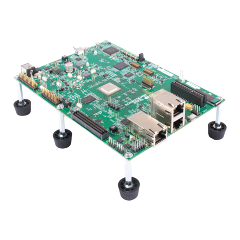
PGA450Q1EVM User’s Guide
8 OTP Memory can be programmed while programming the Development RAM................................... 13
9 Echo Data Stored in FIFO RAM Plotted in Excel ...................................................................... 14
10 LIN Master on GUI......................................................................................................... 16
11 DEVRAM Target Options ................................................................................................. 17
12 OTP Target Options ....................................................................................................... 18
13 DEVRAM STARTUP.A51 Example...................................................................................... 18
14 OTP STARTUP.A51 Example............................................................................................ 18
15 Evaluation Tab Setting .................................................................................................... 19
16 Echo Analog Waveform Output (Channel1), Drive voltage (Channel 2)............................................ 20
17 DAC Output of Filtered Signal (Channel 2) and Drive Voltage (Channel 1)........................................ 21
18 Schematic, LIN ............................................................................................................. 22
19 Schematic, Power.......................................................................................................... 22
20 Schematic, RS232 ......................................................................................................... 23
21 Schematic, USB Controller ............................................................................................... 23
22 Schematic, PGA450-Q1 (TPIC8500-Q1)................................................................................ 24
23 PCB Layout, Bottom ....................................................................................................... 25
24 PCB Layout, Top ........................................................................................................... 25
List of Tables
1 Jumpers....................................................................................................................... 5
2 Default Jumper Settings .................................................................................................... 5
3 Default 0-ΩResistor Setting................................................................................................ 5
4 Transducer and Transformer Manufacturer Part Numbers............................................................. 6
Trademarks
1 Read This First
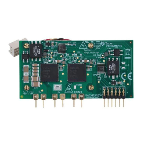
The PGA450-Q1 is an interface device for ultrasonic transducers used in automotive parking assistance
and blind spot detection applications. The device functions as the driver and receiver for a wide range of
transducers with frequency ranges from 40 kHz to 70 kHz. The PGA450-Q1 device incorporates an
analog front end (AFE) and a 8051W microprocessor core. The AFE includes voltage regulators, an
amplifier, an ADC, an oscillator, and a temperature sensor. The PGA450-Q1 device also implements a
LIN 2.1 physical layer for communication. For more details, see the device data sheet.
2 EVM Overview
The features of this EVM are as follows:
• Single power-supply input for basic operation
• Example push-pull transformer and 58-kHz transducer
• LIN master transceiver
• RS-232 transceiver for UART testing and debug
• PC control with a graphical user interface and USB communications board
For a given PGA450Q1EVM installation, the following items apply:
• The PGA450Q1EVM can have either a through-hole or surface-mount transformer installed on it.
When a through-hole transformer is installed, ensure that the case corners are not touching the
surface mount pads.
• The PGA450Q1EVM can be used to drive either a single-ended or push-pull transformer. The selection
of the drive method is achieved through jumper selection.
• The USB communication board 5-V power supply must be enabled for LIN communication to work.
The 5-V power supply provides power to the LIN master transceiver installed on the board.
• In order to communicate with the PGA450-Q1 device using SPI, the 8051W inside the device must be
