Texas Instruments TIDA-050043 Guide

VDD_SOC, VDD_ARM
VDD_HIGH_IN
POR_B
NVCC_DRAM
DRAM_VREF
DRAM Memory Module (DDR)
VDD, VDDQ
VREF
TPS6521815
PMIC
Load Switches 1-3
5 V
1.35 V
1.28 V / 1.33 V
DCDC1
DCDC2
DCDC3
LDO1
IN_BIAS
LS1
IN_DCDCx
IN_LDO1
4
1.8 V
DCDC4
Regulators
IN_LS1
1.8 A
1.8 A
1.8 A
1.6 A
3.3 V
PGOOD
GPO1,3
Digital I/O
SCL
SDA
AC_DET
PWR_EN
nINT
I2Cx_SCL
I2Cx_SDA
GPIO
1
2
3
DC34_SEL
PWR_ON_REQ
VDDA_ADC_3P3, NVCC_3V3
NVCC_1V8
400 mA 2.8 V
to LCD
LS2
IN_LS2
LS3
IN_LS3
CC DCDC6
IN_BU
VDD_SNVS_IN
0
3
USB_OTG_VBUS
i.MX 6ULL, 6UltraLite
Processor
DCDC3
DCDC3
RTT
RTT
1
TIDUEW7–May 2020
Submit Documentation Feedback Copyright © 2020, Texas Instruments Incorporated
Integrated Power Supply Reference Design for NXP i.MX 6ULL
Design Guide: TIDA-050043
Integrated Power Supply Reference Design for
NXP i.MX 6ULL
Description
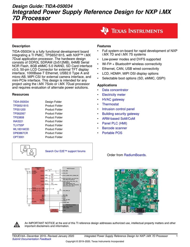
This reference design is a fully functional development
board powering an NXP™ i.MX 6ULL application
processor from a TPS6521815 PMIC. The hardware
design consists of DDR3L SDRAM (512 MB), 32-MB
Serial NOR Flash, 8-GB eMMC 5.0 iNAND, SD Card
interface v3.0, dual-channel 100Base-T Ethernet, 5-
channel USB hub with Type-A ports, micro-AB USB
OTG, mountable LCD screen, and expansion
connector for additional inputs and outputs. This
design is intended to be used as a reference for data
concentrator projects in grid communications or for
any project using the i.MX 6ULL, i.MX 6ULZ, or i.MX
6UltraLite processor that requires evaluation of
alternative power solutions.
Resources
TIDA-050043 Design Folder
TPS6521815 Product Folder
TPS22964C Product Folder
TPS2054B Product Folder
INA3221 Product Folder
DP83849I Product Folder
Ask our TI E2E™ support experts
Features
• Full system-on-board for rapid development of NXP
i.MX 6ULL, i.MX6 ULZ, and i.MX 6UltraLite
systems
• Low-power modes and DVFS supported
• Ethernet, USB wired connectivity
• LCD display included for real-time current
monitoring
• Selectable boot options (SD, eMMC, QSPI)
Applications
•Data Concentrators
•Electricity Meter
•HVAC Gateway
•ARM-based SoM-CoM
•Panel PLC (HMI)
I
I
I
I
I
I
I
Order from RadiumBoards.

System Description
www.ti.com
2TIDUEW7–May 2020
Submit Documentation Feedback
Copyright © 2020, Texas Instruments Incorporated
Integrated Power Supply Reference Design for NXP i.MX 6ULL
An IMPORTANT NOTICE at the end of this TI reference design addresses authorized use, intellectual property matters and other
important disclaimers and information.
1 System Description
TIDA-050043 is first-and-foremost a reference design for powering the NXP i.MX 6ULL processor from the
TPS6521815 PMIC. To show that the PMIC can power the processor, it made the most sense to build a
data concentrator design that can also be used as a full evaluation kit (EVK) board with a variety of
peripheral devices to assist with development of various end equipments. As a result, there are a variety
of wired connections available, as well as multiple BOOT options. The end result of adding all the
peripherals, especially a 5-port USB hub, is that some external load switches have been added to provide
more voltage rails to deliver 5-V USB from the input to the USB hub. Finally, to ensure the entire board is
operational, we developed and tested software using the open-source embedded Linux Yocto SDK to get
started working with this design.
1.1 Key System Specifications
Table 1. Key System Specifications
PARAMETER SPECIFICATIONS DETAILS
Processor i.MX 6ULL, ARM Cortex-A7 Applications Processor,
MCIMX6Y2CVM08AB Section 2.2.1
PMIC TPS6521815 user-programmable PMIC with automatic sequencing and
DVFS Section 2.3.1
Memory 4-Gb DDR3L (512 MB), 256-Mb QSPI NOR-Flash (32 MB), 8GB
eMMC 5.0, SD v3.0 interface Section 2.2.2
Ethernet Dual-port ethernet interface - TI DP83849I PHY and 0845-2R1T-E4
RJ45 jack from Bel Fuse Section 2.3.2
Debug method (USB-to-UART) FTDI FT230X is required to implement USB to serial UART conversion Section 2.2.3
USB ports 5x USB Type-A ports (USB2517I-JZX hub IC) and 1x micro-AB port for
USB OTG (Amphenol 10104111-0001LF) Section 2.2.4
LCD display RGB TFT 40-pin connector (Molex 54132-4062) for LCD display
(Newhaven Display NHD-2.4-240320CF-CTXI#-F), compatible with
touch-screen controller (TI TSC2046IPWR) Section 2.2.5
JTAG header JTAG connection to i.MX 6ULL processor with 50-mil pitch, 10-pin
header Section 2.2.6
USB2ANY header Debug method for PMIC separate from processor I2C bus. Provided by
USB2ANY (standard 100-mil pitch, 10-pin header) Section 2.2.7
Current monitoring 2x TI INA3221 devices are used to monitor current through 6 rails in
the system Section 2.3.3
Operation with Coin Cell Coin cell for i.MX 6ULL SNVS input. Using DCDC6 of TPS6521815
PMIC, system always powers SNVS before full power-up sequence
begins.
Section 2.3.4
Tactile inputs, visual feedback Push-buttons and status LEDs connected to GPIOs of the processor to
assist with debugging software Section 2.2.8
100Base-T
(2x1 RJ-45 Connector) µ-SD Card Slot
USB OTG
(micro-AB)
ESD Protection
ESD8472MU
NOR Flash 32MB
MT25QU256ABA1EW7
i.MX 6ULL
Applications
Processor
(MCIMX6Y2CVM08AB)
BOOT MODE
SELECT (4POS)
STATUS LEDs
USER 1&2,
MX ON/OFF
ESD Protection
PUSB3F96
GPIOs QSPIA t4 bit
eMMC t8 bit
HS200
DDR3L t16 bit
GPIOs,
MX-ON/OFF
2 - RMII USB Debug
FT230XS
ESD Protection
ESD8472MU
USB
Debug Port
USB2.0 x1
BOOT MODE
I/P
POR_B
PMIC
TPS6521815
VIN: 5-V DC
Current Sense
INA3221 To Processor I2C
USB2.0 x1
DDR3L 512MB
MT41K256M16TW-107:P
eMMC 8GB
MTFC8GAKAJCN-4M
SDIO t4 bit
ESD Protection
ESD8472MU
UART1 x 1
BOOT MODE
SELECT (2POS)
BOOT MODE
I/P
USB HUB
USB2517-JZX
Supervisory
TPS3808G25
RESET
SWITCH
POR_B
PMIC_ON_REQ
WDOG_B
PMIC_ON_REQ
WDOG_B
Power and Monitoring Section
USB2.0 5-Port
(2 - 2x1 Type-A & 1 tType-A)
LCD Screen
USB2.0 x1
8/16-bit
Parallel
ETHERNET PHY
DP83849I
ESD Protection
PUSB3F96
ESD Protection
ESD8472MU (5Nos)
www.ti.com
System Overview
3
TIDUEW7–May 2020
Submit Documentation Feedback Copyright © 2020, Texas Instruments Incorporated
Integrated Power Supply Reference Design for NXP i.MX 6ULL
2 System Overview
2.1 Block Diagram
Figure 1. TIDA-050043 Block Diagram

System Overview
www.ti.com
4TIDUEW7–May 2020
Submit Documentation Feedback
Copyright © 2020, Texas Instruments Incorporated
Integrated Power Supply Reference Design for NXP i.MX 6ULL
2.2 Design Considerations
This design is intended to show the ability of the TPS6521815 PMIC to provide power to the i.MX 6ULL
processor and all of the peripheral ICs in a variety of designs. To verify this, we had to populate all of
these other ICs on the design, starting with the processor. All other devices necessary to build an
operational data concentrator or general-purpose evaluation kit are included in this section. The PMIC and
other TI devices used in this design are described in Section 2.3.
2.2.1 Processor – i.MX 6ULL Applications Processor
The main component of this design is the NXP i.MX 6ULL processor. It is a single-core Arm®Cortex®-A7
16-bit processor. Dynamic voltage and frequency scaling (DVFS) is a highlight of the processor, wherein
the processor can change the core voltage with respect to the processing power required. The multimedia
performance of the processor is enhanced by a multilevel cache system, an ARM NEON media processor
engine (MPE) co-processor, a programmable smart DMA (SDMA) controller, an asynchronous audio
sample rate converter, an electrophoretic display (EPD) controller, and a pixel processing pipeline (PXP)
to support 2D image processing, including color-space conversion, scaling, alpha-blending and rotation.
DDR3L, eMMC, SD, QSPI, UART, and I2C are the processor interfaces we are using in this design.
DESCRIPTION MFG. PART NUMBER
iMX6ULL, ARM Cortex-A7 Application
Processor, 792MHz, MAPBGA-289 NXP MCIMX6Y2CVM08AB

i.MX6 ULL
DRAM_CS0_B
DRAM_RAS_B
DRAM_CAS_B
DRAM_SDWE_B
DRAM_ODT0
DRAM_CS1_B
DRAM_ODT1
DRAM_SDCKE1
DRAM_ZQPAD
MT41K256M16TW-107:P
DQ[15:0]
LDQS/LDQS#
UDQS/UDQS#
LDM/UDM
CS#
RAS#
CAS#
WE#
ODT
ZQ
NC1
NC2
NC3
NVCC_DRAM_1V35 DRAM_VREF
NVCC_DRAM DRAM_VREF
NVCC_DRAM_2P5
DRAM_DATA[15:00]
DRAM_SDQS0_P/N
DRAM_SDQS1_P/N
DRAM_DQM[1:0]
VDD_HIGH_CAP
240 E
240 E
10 K
DRAM_ADDR[15:00]
DRAM_ADDR[15]
DRAM_SDBA[2:0]
DRAM_SDCLK0_P/N
DRAM_SDCKE0
DRAM_RESET_B
A[14:0]
NC4
BA[2:0]
CK/CK#
CKE
RESET#
VDD VDDQ
NVCC_DRAM_1V35
VREFDQ VREFCA
DRAM_VREF
NVCC_DRAM_1V35
1.5 K
1.5 K
DRAM_VREF
VSS/VSSQ
VSS
DRAM_SDCLK0_P
DRAM_SDCLK0_N
470 E
DRAM_SDQS0_P
2.2 pF
DRAM_SDQS0_N
DRAM_SDQS1_P
DRAM_SDQS1_N
2.2 pF
www.ti.com
System Overview
5
TIDUEW7–May 2020
Submit Documentation Feedback Copyright © 2020, Texas Instruments Incorporated
Integrated Power Supply Reference Design for NXP i.MX 6ULL
2.2.2 i.MX 6ULL Memory Interfaces
This project makes use of i.MX 6ULL processor’s four different external memory interfaces using 4-Gb
DDR3L (512 MB), 256-Mb QSPI NOR-Flash (32 MB), 8-GB eMMC 5.0, and SD v3.0.
2.2.2.1 DDR3L
i.MX 6ULL has a dedicated DDR memory controller which supports 16-bit LP-DDR2-800, DDR3-800, and
DDR3L-800, all of which can operate up to 800 MT/s data rate. This design is provided with single 4-Gb
x16 (512 MB) DDR3L memory. Micron’s MT41K256M16TW-107:P is a 4-Gb DDR3L SDRAM used in this
design. The memory interface comprises of single channel of 16-bit data signals, along with command and
address signals. The DDR interface is shown in Figure 2.
DESCRIPTION MFG. PART NUMBER
IC, DDR3L SDRAM, 512MB, x16bit, 1866 MT/s, FBGA-
96 Micron MT41K256M16TW-107:P
Figure 2. DDR3L Interface

DAT[0-7]
CLK
CMD
VCCQ
10 kŸ
SD2_DATA[0-7]
SD2_CLK
SD2_CMD
SD2_RESET# RESET#
10Ÿ
VCC
3V3 1V8
1V8
MTFC8GAKAJCN-4M IT
i.MX 6ULL
VSS
10 Ÿ
DS
NVCC_NAND
1V8
Note: NVCC_NAND and VCCQ needs to be 1V8 for HS200
Mode. CLK/CMD/DATA lines impedance need to be 50 Ÿ
VSS
10 kŸ
QSPIA_DATA0
QSPIA_DATA1
QSPIA_DATA2
QSPIA_SCLK
MT25QU256ABA1EW7-0SITi.MX 6ULL
NVCC_NAND
1V8
QSPIA_DATA3
QSPIA_SS0_B
DQ0
DQ1
W#/DQ2
C
VCC
1V8
HOLD#/DQ3
S#
VSS
1V8
10 kŸ
VSS
System Overview
www.ti.com
6TIDUEW7–May 2020
Submit Documentation Feedback
Copyright © 2020, Texas Instruments Incorporated
Integrated Power Supply Reference Design for NXP i.MX 6ULL
2.2.2.2 Quad SPI NOR Flash
The i.MX 6ULL processor has a Serial NOR Flash interface (QSPI). This design uses Micron’s
MT25QU256ABA1EW7-0SIT Serial NOR Flash memory with a density of 256 Mb (32 MB) supports a
clock frequency of 166 MHz for data through-put up to 90 MBps at DTR with an operating voltage of 1.7 V
to 2.0 V, and the interface diagram of this Flash IC with the processor is shown in Figure 3.
DESCRIPTION MFG. PART NUMBER
IC, NOR Flash, 32MB, 133MHz, SPI, 1.7-2V, W-PDFN-8 Micron MT25QU256ABA1EW7-0SIT
Figure 3. QSPI NOR Flash Interface
2.2.2.3 eMMC iNAND
The i.MX 6ULL processor supports eMMC versions 4.4, 4.41, and 4.5. This design uses Micron's 8-GB
MTFC8GAKAJCN-4M IT, an eMMC version 5.0 memory device. The eMMC version 5.0 specification
indicates is backwards compatibility, allowing it to work correctly with the processor. The data transfer
speed used is HS200 mode with 1.8-V I/O voltage. The interface diagram of eMMC with the processor is
shown in Figure 4.
DESCRIPTION MFG. PART NUMBER
IC, eMMC 5.0, 8GB, x8bit, 52MHz, VFBGA-153 Micron MTFC8GAKAJCN-4M IT
Figure 4. eMMC Interface

i.MX 6ULL µSD CONNECTOR
693071010811
SD1_DATA[0:3]
SD1_CLK
GPIO3_IO6
GOIO3_IO5
SD1_CMD
CD#
WP#
CMD
DATA[0:3]
CLK
22 Ÿ
22 Ÿ
ESD
NVCC_SD1
10 kŸ
VDD
VDD_3V3_PERI
VSS
22 Ÿ
VSS
NVCC_SD1
NVCC_SD
www.ti.com
System Overview
7
TIDUEW7–May 2020
Submit Documentation Feedback Copyright © 2020, Texas Instruments Incorporated
Integrated Power Supply Reference Design for NXP i.MX 6ULL
2.2.2.4 SD Card Connector
i.MX 6ULL supports SD3.0 so in this design there is a micro-SD card connector provided. The power
supply to the SD card is 3.3 V and the wiring for the SD Card interface is shown in Figure 5.
DESCRIPTION MFG. PART NUMBER
Conn, uSD card socket, 1x1, Push-Push, RA, SMD Wurth Elektronik, Inc 693071010811
Diode, ESD-Bidir, 5.5V, SOD-882D NXP PESD5V0F1BL
Figure 5. SD Card Power and Connector

FT230XS
UART1_TX_DATA
FT_TXD
FT_RXD
UART1_RX_DATA
i.MX 6ULL
VCCIOVCC
VDD_3V3 _PERI
USB_DM
USB_DP D+
D- D-
D+
GND
ECMF02-2
USB_5V0
10118193-0001LF
27 Ÿ
GND AGND
CBUS0
47 pF
RESET#
VDD_3V3 _PERI
10 kŸ
NOTE : Need to pull down CTS on processor side
CTS#
USB_5V0
4.7 kŸ
10 kŸ
VDD_3V3_PERI
4.7 kŸ
10 kŸ
VSS
System Overview
www.ti.com
8TIDUEW7–May 2020
Submit Documentation Feedback
Copyright © 2020, Texas Instruments Incorporated
Integrated Power Supply Reference Design for NXP i.MX 6ULL
2.2.3 USB to UART Converter
There is a USB to Serial (UART) interface in the design. To implement this feature, the FT230X chip from
FTDI is used which is a USB to dual port RS232 converter. The detailed diagram of interconnection is
shown in Figure 6.
DESCRIPTION MFG. PART NUMBER
IC, FT230X, USB to UART Converter, SSOP-16 FTDI Chip FT230XS
IC, ECMF02-2, Dual-line CM Filter with ESD Protection,
5GHz, WLCSP-5P ST Microelectronics ECMF02-2BF3
Conn, USB Micro-B Receptacle, 1x1, RA, SMD FCI - Amphenol ICC 10118193-0001LF
Figure 6. USB to Serial UART Interface With FT230X

i.MX 6ULL
NVCC_UART
USB_OTG1_ID
ESD
Diode
USB Hub
USB2517
24-MHz
Crystal Oscillator
XTALI
XTALO
USB Load Switch
TPS2054B
OC1#
OC2#
OC3#
OC4#
USB 2.0
Type-A Port
D+
D±
VCC
GND
PRTPWR3
PRTPWR4
PRTPWR1
PRTPWR2
OUT1
OUT2
OUT3
OUT4
USB Load Switch
MIC2026
OUTA
OUTB
GND
ENA
FLAGA#
ENB
FLAGB#
IN
5V0
EN1
EN2
10 k
10 k
10 k
10 k
3V3
USB 2.0
Type-A Port D+
D±
VCC
GND
DLW21HN
Choke Coil
ESD
Diode
DLW21HN
Choke Coil
USB_OTG1_VBUS
USB_OTG2_VBUS
USB_OTG2_DP
USB_OTG2_DN
USB_OTG1_DP
USB_OTG1_DN
ESD
Diode
OUT1
I2C2_SDA
I2C2_SCL
10 k
10 k
3V3
USBDN1_DP
USBDN1_DM
USBDN2_DP
USBDN2_DM
USBDN3_DP
USBDN3_DM
USBDN4_DP
USBDN4_DM
USBDN5_DP
USBDN5_DM
PRTPWR5
USBUP_DP
USBUP_DM
SDA
SCL
10 k
10 k
3V3
FLAGA#
FLAGB#
OCS1#
OCS2#
OCS3#
OCS4#
VDD33, VDDA33V,
VDD33PLL, VDD33CR
10 k
5V0
USB_OTG2_ID
USB_OTG1_PWR
USB_OTG1_OC
USB
micro-AB Port
D+ D±
VCC
ID
OUTB
VSS
ESD
Diode
DLW21HN
Choke Coil
DLW21HN
Choke Coil
DLW21HN
Choke Coil
DLW21HN
Choke Coil
ESD
Diode
ESD
Diode
USB 2.0
Type-A Port
D+
D±
VCC
GND
OUT2
USB 2.0
Type-A Port
D+
D±
VCC
GND
OUT3
USB 2.0
Type-A Port
D+
D±
VCC
GND
OUT4
3V3
OCS5#
IN
5V0
www.ti.com
System Overview
9
TIDUEW7–May 2020
Submit Documentation Feedback Copyright © 2020, Texas Instruments Incorporated
Integrated Power Supply Reference Design for NXP i.MX 6ULL
2.2.4 USB Ports
This design uses the processor's two USB interfaces, where the primary USB OTG1 interface connects
directly to the micro-AB port and USB OTG2 acts as a host only, connecting to a USB Hub. The
USB2517I is a 7-port USB hub that multiplexes the USB data from OTG2 and distributes the data to 5
Type-A receptacles. The block diagram shows both USB HUB and OTG interfacing with the processor.
The wiring of the USB interfaces is shown in Figure 7.
DESCRIPTION MFG. PART NUMBER
USB Hub Section
Conn, USB 2.0, Type-A, Receptacle, 1x1, Shielded, RA,
TH TE Connectivity 1-1734775-1
Conn, USB Type-A Receptacle, 2x1, Shielded, Stacked,
RA, TH TE Connectivity ZX62D-AB- 5P8(30)
Filter, Choke coil, CM, 90E, 330mA, Signal Line, SMD Murata DLW21HN900SQ2L
IC, TPS2054B, Quad Current-Limited Power-Distribution
Switch, SOIC-16 Texas Instruments TPS2054BDR
IC, USB2517I, USB HUB, 7-Ports, QFN-64 Microchip USB2517I-JZX
USB OTG Section
Conn, USB 2.0 Micro AB Receptacle, 1x1, Shielded, RA,
SMD FCI - Amphenol ICC 10104111-0001LF
Filter, Choke coil, CM, 90E, 330mA, Signal Line, SMD Murata DLW21HN900SQ2L
IC, MIC2026, Dual Channel Power Distribution Switch,
SOIC-8 Microchip MIC2026-1YM
Figure 7. USB Interface

Optional
i.MX 6ULL
LCD_WR_RWn
LCD_RD_E
GPIO
40-pin LCD
FPC Connector
54132-4062
SPI_MOSI
Touch Screen
Controller
TSC2046
DATA[15..0]
SPI_MISO
LCD_DATA[15..0]
LCD_RS
SPI_CS#
SPI_CLK
LCD_RESET/WDOG
/WR
/RD
D/C
/RES
CS#
IMO
10 k
10 k
VDD IOVDD LEDA
VDD_3V3 VDD_1V8 VDD_3V3
VDD_2V8
OR
NVCC_LCD
VDD_1V8
YU
XL
YD
XR
VSS GND LED_K
System Overview
www.ti.com
10 TIDUEW7–May 2020
Submit Documentation Feedback
Copyright © 2020, Texas Instruments Incorporated
Integrated Power Supply Reference Design for NXP i.MX 6ULL
2.2.5 LCD Screen Connector
This design has a mountable LCD screen. The i.MX 6ULL processor's LCD interface can be used to
control a wide range of display devices varying in size and capability. Many of these displays have an
asynchronous parallel MPU interface for command and data transfer to an integrated frame buffer. There
are other popular displays that support moving pictures and require the RGB interface mode (called
DOTCLK interface in this document) or the VSYNC mode for high-speed data transfers. In addition to
these displays, it is also common to provide support for digital video encoders that accept ITU-R BT.656
format. The goal is to select an LCD screen that is suitable for the application and compatible with the
processor.
The Newhaven Display NHD-2.4-240320CF-CTXI#-F backlight and LCD screen selected for this design
can make use of the already available 3.3 V and 1.8 V supply voltages so we can eliminate the need for
additional voltage regulators. Additionally, this display is compatible with the processor and exceeds the
simple requirements of a data concentrator application. The LCD interface is connected through 40-pin
FPC connector. The connection diagram of the LCD interface is shown in Figure 8.
(1) The touch-screen controller is optional and can be added to take advantage of the touch-screen capability of the display, but
TSC2046 is not mounted in this design.
DESCRIPTION MFG. PART NUMBER
Display, TFT LCD, 240x320, 8/16-bit Parallel MPU
Interface Newhaven Display NHD-2.4-240320CF-CTXI#-F
Conn, FPC, Receptacle, 1x40, 0.5mm, 0.5A, Bottom
Contact, RA, SMD Hirose Electric Co Ltd FH40-50S-0.5SV
IC, TSC2046, Touch Screen Controller, TSSOP-16 Texas Instruments TSC2046IPWR(1)
Figure 8. LCD Interface From i.MX 6ULL Processor to Connector
2.2.6 JTAG Header
The JTAG connections match the requirements of the i.MX 6ULL for direct access to the processor for
programming and debugging.
DESCRIPTION MFG. PART NUMBER
Connector, Berg strip, 2x5, 1.27mm, 1A, ST, SMD FCI 20021121-00010*4LF

PMIC
TPS6521815
GPIO
SPI:MISO
GPIO
SPI:CS
SPI:MOSI
SPI:SCLK
SCL
SDA
I2C1:SCL
I2C1:SDA
2
4
6
8
10 9
7
5
3
1
10-Pin USB2ANY Connector
www.ti.com
System Overview
11
TIDUEW7–May 2020
Submit Documentation Feedback Copyright © 2020, Texas Instruments Incorporated
Integrated Power Supply Reference Design for NXP i.MX 6ULL
2.2.7 USB2ANY Header
USB2ANY is TI MCU-based adapter intended to allow a computer to control an electronic evaluation
module (EVM) via a USB connection. In this design, the I2C interface of USB2ANY is used to externally
monitor, control, and or re-program the internal registers of PMIC. The wiring of the USB2ANY header is
shown in Figure 9.
DESCRIPTION MFG. PART NUMBER
Connector, Berg strip, 2x5, 2.54mm, ST, SMD Samtec TSM-105-01-T-DV
Figure 9. USB2ANY Header Connections to PMIC I2C Pins
2.2.8 Functional Switches and Status LEDs
There are two functional multi-purpose push buttons connected to GPIOs configured as inputs on the
processor that can be used for software developers to test applications developed using this board. Three
LED are connected to three GPIOs of the processor to indicate the status of processes that are running,
completed, or may have failed. Both the push-buttons and status LEDs can be used for debugging or to
provide tactile inputs and visual feedback to the user. These connections are shown in Figure 10.
Figure 10. GPIO Connections to Push-buttons and LEDs
2.2.9 GPIO Expansion Connector
All un-used GPIO pins on the i.MX 6ULL processor are routed out to an expansion header, which is also
capable of providing 1.8 V, 3.3 V, and 5 V to a daughter card PCB.

TPS6521815 i.MX 6ULL
SCL I2C1_SCL
I2C1_SDA
SDA
PWR_EN
SNVS_PMIC_ON_REQ
nINT
nWAKEUP
nPFO
PGOOD
AC_DET
PB#
PFI
GPIO1_IO9
GPIO1_IO8
GPIO3_IO9
POR_B
5 V
NN
5 V
N
DC34_SEL 0 Ÿ
0 Ÿ
VDD_3V3
nINT nPFO nWAKEUP
VDD_3V3
4.7 kŸ
10 kŸ
PGOOD
300 kŸ
PWR_EN
CCM_PMIC_STBY_REQ
GPIO3
10 kŸ
10 kŸ
10 kŸ
4.7 kŸ
System Overview
www.ti.com
12 TIDUEW7–May 2020
Submit Documentation Feedback
Copyright © 2020, Texas Instruments Incorporated
Integrated Power Supply Reference Design for NXP i.MX 6ULL
2.3 Highlighted Products
2.3.1 TPS6521815 - Power Management IC
The TPS6521815 device is a Power Management IC (PMIC) specifically designed to support Arm Cortex
processors like the i.MX 6ULL from NXP. The PMIC is a good fit for applications powered from a 5-V
supply or a Li-Ion battery. The IC consists of three adjustable step-down (buck) converters, one buck-
boost converter, one adjustable LDO regulator and three load switches with two selectable current limit.
The PMIC supports undervoltage lockout (UVLO), over-temperature warning and shutdown, separate
power-good output for all regulators, programmable power sequencing for all regulators, and an I2C
interface for register reading and writing to the device. The full power architecture of this design is shown
in Figure 15.
The I/O connections between the processor and the TPS6521815 PMIC are shown in Figure 11, as well
as analog and digital input pins on the PMIC.
Figure 11. TPS6521815 PMIC I/O Wiring to i.MX 6ULL Processor

3V3 3V3
NVCC_ENET
ENET1_TX_EN
ENET1_TX_DATA0
ENET1_TX_DATA1
33 Ÿ
33 Ÿ
33 Ÿ
i.MX 6ULL
ENET_MDC
ENET_MDIO
NVCC_GPIO
2x1 RJ45
with internal
magnetics
3V3
ENET_MDIO_A 1.5 kŸ
RXER_A
2.2 kŸ
RXER_B
2.2 kŸ
2.2 kŸ
VSS
ENET1_RX_EN
ENET1_RX_DATA0
ENET1_RX_DATA1
33 Ÿ
33 Ÿ
33 Ÿ
33 Ÿ
ENET1_RX_ER
IOVDD
3V3
TXD0_A
TXD1_A
TXEN_A
RXD1_A
MDC
MDIO
ANAVDD
3V3
MEDIA
DEPENDENT
INTERFACE
ESD
PUSB3F96
X1
50-MHz OSC
ASFL1-50.000-MHZ-EC-T
CRSDV_A
RXD0_A
RXER_A
ENET2_RX_EN
ENET2_RX_DATA0
ENET2_RX_DATA1
33 Ÿ
33 Ÿ
33 Ÿ
33 Ÿ
ENET2_RX_ER
TXD0_B
TXD1_B
TXEN_B
RXD1_B
MEDIA
DEPENDENT
INTERFACE
ESD
PUSB3F96
VSS
CRSDV_B
RXD0_B
RXER_B
ENET2_TX_DATA0
ENET2_TX_DATA1
33 Ÿ
33 Ÿ
33 Ÿ
ENET2_TX_EN
PHY ADDR:
0b00000
PHY ADDR:
0b00001
3V3
ED_EN_A
ED_EN_B
2.2 kŸ
RXD0_A
2.2 kŸ
2.2 kŸ
DP83849I
RBIAS
.
MII_MODE_A
MII_MODE_B
2.2 kŸ
www.ti.com
System Overview
13
TIDUEW7–May 2020
Submit Documentation Feedback Copyright © 2020, Texas Instruments Incorporated
Integrated Power Supply Reference Design for NXP i.MX 6ULL
2.3.2 DP83849I - Dual Ethernet PHY
i.MX 6ULL supports two 10/100Mbps (MII/RMII) Ethernet interfaces. This design requires two 100 Base-T
Ethernet ports so the DP83849I-Dual Ethernet PHY is used in this design. This Ethernet PHY supports
two RMII interface and able to work from a single 3.3V supply. The PHY needs an external 50MHz
oscillator to function properly. To connect MDI to the Cat5e cable, we used a dual RJ45 connector with
internal magnetics from Wurth Elektronik. The addresses for the two separate PHYs are listed in Table 2.
Table 2. PHY Addresses
PHY Number PHY Address
PHY1 0b00000
PHY2 0b00001
The Ethernet interface connections are shown in Figure 12.
DESCRIPTION MFG. PART NUMBER
IC, DP83849I, Dual Port, 10/100 Ethernet PHY
Transceiver, TQFP-80 Texas Instruments DP83849IVSX/NOPB
Connector, RJ45 Jack with Magnetics, Shielded,
LED(G/Y, G/Y), RA, TH Wurth Elektronik 7499111446
Figure 12. Ethernet Interface With DP83849I PHY

i.MX 6ULL
TPS6521815
INA3221
INA3221
VIN+1 VIN-1
VIN+2 VIN-2
VIN+3 VIN-3
SDA
SCL
A0
VIN+1 VIN-1
VIN+2 VIN-2
VIN+3 VIN-3
SDA
SCL
A0
VS
GND
GND
VS
VPU
VP
U
VDD_3V3
VDD_3V3
VDD_3V3
10K
DCDC1
DCDC2
DCDC3
DCDC4
LS1
LS2 & 3
VDD_SOC_ARM_IN
NVCC_DRAM
VDD_HIGH_IN_3V3
VDD_1V8
VDD_3V3
USB_OTG_VBUS
I2C2_SDA
I2C2_SCL
I2C2_SDA
I2C2_SCL
System Overview
www.ti.com
14 TIDUEW7–May 2020
Submit Documentation Feedback
Copyright © 2020, Texas Instruments Incorporated
Integrated Power Supply Reference Design for NXP i.MX 6ULL
2.3.3 INA3221 - Current Monitor
To measure the live current information, a current sense circuit is inserted in series with the power nets
from the PMIC to the processor. The current sensing is done with the INA3221 device. There are two
devices used to monitor all the TPS6521815 PMIC power rails. The wiring is shown in Figure 13. The
address pin A0 of the INA3221 device needs to be terminated according to Table 3.
Figure 13. INA3221 Current Sensor Wiring From PMIC to Processor
(1) Both of the I2C lines, SDA and SCL, require a pull-up resistor. A resistance of 2.2-kΩis used to pull-up these
open-drain signals to 3.3V
Table 3. INA3221 I2C Slave Address Options
7-BIT BINARY ADDRESS 7-BIT HEX ADDRESS ADDR PIN TERMINATION
1000000b 0x40 GND
1000001b 0x41 VS
1000010b 0x42 SDA
1000011b 0x43 SCL

VDD_SNVS_IN
i.MX 6ULL TPS6521815
Push-Button
Controller
PMIC_ON_REQ
POR_B
ONOFF
WDOG1_ANY
TS
PB
GND
RESET#
RESET#
PWR_EN
PGOOD
nPFO
M15
PB#
TPS342x
Diodes
BUFFER
VDD_NVCC_3V3
EN
LS1
www.ti.com
System Overview
15
TIDUEW7–May 2020
Submit Documentation Feedback Copyright © 2020, Texas Instruments Incorporated
Integrated Power Supply Reference Design for NXP i.MX 6ULL
2.3.4 Reset Scheme
The reset scheme for this project is shown in Figure 14. The DCDC6 low-power buck regulator from
TPS6521815 provides the VSNVS voltage from the coin-cell. If the coin-cell is not inserted, the PMIC will
still provide VSNVS supply first through SYS_BU input. This is critical to ensure the power-up sequence is
correct. When VSNVS is stable along with all the power outputs, the PGOOD pin will de-assert the Power-
ON Reset (POR_B).
A reset push-button is connected to the watchdog output of the i.MX 6ULL processor in a wire-OR
configuration, which goes into the PB input of a TPS342x push-button controller. The push-button
controller can override the enable signal (PWR_EN) to the PMIC and the POR_B input on the processor
simultaneously, forcing the system to reset. To shut the system down completely, a separate push-button
connected to the ONOFF pin of the processor is used.
Figure 14. Reset Scheme
2.3.5 TPS2054B, TPS22964C - Auxiliary Load Switches
Figure 15 shows the full power architecture. Each peripheral device added to a design may require
additional power in addition to what is required by the processor. For this design, we had to add load
switches (TPS22964C, TPS2054B) for powering the multiple USB ports and an additional load switch
(TPS22964C) for 3.3 V peripherals for the MIPI CSI. Both of these voltages are already available in the
design: 5 V is the main input power supply voltage and 3.3 V is generated by DCDC3 of the TPS6521815.
As a result, only load switches were added to enable and disable these supply rails, as opposed to adding
additional DC-DC or LDO voltage regulators.
Finally, it is sometimes necessary to terminate DDR memory. DDR termination provides a supply (0.675
V) that is half the voltage of the main supply (1.35 V) with the ability to sink or source current. If only one
channel of DDR is used, the current consumption is low, or the routing is point-to-point, then tapping off
the center of an evenly matched voltage divider may be sufficient. In other cases, a DDR terminator power
IC is needed. For this design, we used the matched resistor divider option to terminate the single DDR3L
memory IC in the system.

i.MX 6ULL
TPS6521815
PMIC
VIN
5-V DC
Coin
Cell VDD_SNVS_IN
VDD_SOC, VDD_ARM
NVCC_DRAM
VDD_HIGH_IN
NVCC_1V8
VDDA_ADC_3P3, NVCC_3V3
USB_OTG_VBUS
DCDC5
25 mA
DCDC6
25 mA
DCDC1
1.8 A
DCDC2
1.8 A
DCDC3
1.8 A
DCDC4
1.6 A
LDO1
400 mA
LS1
380 mA
LS2
900 mA
LS2
920 mA
Load Switch
TPS22964C
Load Switch
TPS2054B
USB Power
Switch
4x USB
Host
2 x USB
Host & OTG
SD
Card
eMMC USB-to-
UART
LCD Screen
DDR3L
LCD
Serial NOR Flash
USB Hub
3.0 V, 1 mA
1.275 V / 1.325 V, 500 mA
1.35 V, 50 mA
3.3 V, 200 mA
1.8 V,
100 mA
3.3 V,
150 mA
5.0 V,
50 mA
5.0 V,
1 A
1.35 V,
241 mA
3.3V,
947 mA
VREF
VDD_HIGH_IN
VDD_HIGH_IN
VDD_HIGH_IN
GPIO1
GPIO1
Load Switch
TPS22964C
5.0 V,
2 A
RTEthernet
PHY
eMMC
LCD Screen
LCD Screen
SD Card
Power Mux
2.8 V, 15 mA
3.3 V, 200 mA
3.3 V
1.8 V
1.8 V, 150 mA
3.3 V, 747 mA
RT
System Overview
www.ti.com
16 TIDUEW7–May 2020
Submit Documentation Feedback
Copyright © 2020, Texas Instruments Incorporated
Integrated Power Supply Reference Design for NXP i.MX 6ULL
Figure 15. TIDA-050043 Full Power Architecture

www.ti.com
System Overview
17
TIDUEW7–May 2020
Submit Documentation Feedback Copyright © 2020, Texas Instruments Incorporated
Integrated Power Supply Reference Design for NXP i.MX 6ULL
2.4 System Design Theory
The full power architecture is the result of carefully estimating the power consumed by ICs on the board
and peripherals that can be connected to the board. The ideal power sequencing of the i.MX 6ULL
processor must be known to ensure the power sequencing of the TPS6521815 is correct. The I2C chain
must be drawn in its entirety to ensure there are no I2C address conflicts. The BOOT Mode settings must
be mapped to boot the processor using the intended memory storage IC. And finally, PCB floor planning
must be completed to make sure the layout of the board is reasonable. All of this system design theory is
taken into consideration in this section.
2.4.1 Power Estimation
This design is powered from a 5-V adapter. This 5 V is the main power supply to the TPS6521815 device.
The PMIC will generate 6 different voltages: 1.275 V/1.325 V with dynamic voltage scaling (DVS), 1.35 V,
3.3 V, 1.8 V, 2.8 V, and a 2.4 V to 3.0V always-on supply for SNVS. The load switches LS2 and LS3 are
used to power USB slave devices with 5.0 V. The estimated current consumption for each rail is listed in
Table 4.
Table 4. System Power Estimation
VOLTAGE (V) SUPPLY IC, RAIL NAME SUPPLY
CURRENT
(mA)
LOAD IC, RAIL NAME CURRENT
(mA) POWER (mW)
1.275/1.325 TPS6521815, DCDC1 1800 iMX6 VDD_SOC_IN 500 663
1.35 TPS6521815, DCDC2 1800 iMX6 NVCC_DRAM 50 67.5
DDR3L VDD/VDDQ 290 392
3.3 TPS6521815, DCDC3 1800 iMX6 VDD_HIGH_IN 200 660
iMX6 NVCC_3V3 150 495
DP83849I IOVDD, ANA33VDD 50 165
IOVDD_LCD,
VDD_LCD_BCKLIGHT 200 660
eMMC 40 132
SD Card 200 660
FT230X 10 33
USB Hub (USB2517) 460 1518
1.8 TPS6521815, DCDC4 1600 i.MX7 NVCC_1V8 100 489
eMMC 100 180
NOR Flash 35 63
2.8 TPS6521815, LDO1 400 VDD_LCD 200 560
5 TPS6521815, LS2/3 &
TPS22964C
into TPS2054B & MIC2026
1820 & 2000
into 4x500 &
2x500
6x USB2 Ports 3000 15000
USB_OTG_VBUS 50 350
2.4 - 3.0 TPS6521815, DCDC6 25 iMX6 VDD_SNVS_IN 1 3
Total Estimated Power 22.1 W

POR_B
(PGOOD)
USB_OTGx_VBUS
NVCC_NAND
(1.8 V, DCDC4)
NVCC_XXX, VDDA_ADC_3P3,
VDD_PERI_3V3, VDD_2V8
(LS1, LDO1, 3V3 switch)
NVCC_DRAM
(1.35 V, DCDC2)
VDD_SOC_IN
(1.325/1.27 V, DCDC1)
VDD_HIGH_IN
(3.3 V , DCDC3)
VDD_SNVS_IN
(3 V, coin cell/DCDC6)
T1>=0
T2>=0
T3>0
T4>0
T5>0
T6>0
T7>0
(5 V, LS2, LS3 & LS4)
VDD_SNVS_IN
(3 V, coin cell/DCDC6)
VDD_SOC_IN
(1.325 V/1.27 V, DCDC1)
VDD_HIGH_IN
(3.3 V, DCDC3)
NVCC_DRAM
(1.35 V, DCDC2)
NVCC_XXX, VDDA_ADC_3P3,
VDD_PERI_3V3 (3.3 V), VDD_2V8
(LS1, LDO1, 3V3 switch)
NVCC_NAND
(1.8 V, DCDC4)
USB_OTG_VBUS 1& 2
(5 V, LS2, LS3, LS4)
POR_B
(PGOOD)
t1>0
t2>0
t3>0
t4>=0
t5>=0
t6>0
t7>0
System Overview
www.ti.com
18 TIDUEW7–May 2020
Submit Documentation Feedback
Copyright © 2020, Texas Instruments Incorporated
Integrated Power Supply Reference Design for NXP i.MX 6ULL
2.4.2 Power Sequencing
The processor power-up sequencing is shown in Figure 16. First the VDD_SNVS needs to turn on before
any other power supply. For our design, VDD_SNVS is powered through a coin cell connected to the CC
pin of the TPS6521815 PMIC, and the DCDC6 supply will always be the first PMIC supply rail to turn on.
Once SNVS voltage is stabilized, then VDD_HIGH_IN should turn on because VDD_HIGH_IN should be
enabled before VDD_SOC_IN for the i.MX 6ULL processor. After VDD_SOC_IN, NVCC_DRAM is turned
on for the DDR3L memory followed by 3.3 V for I/O and analog along with 2.8 V for the LCD screen. The
final supply to turn on is the 1.8-V I/O rail. Once all these voltages are enabled and within regulation, there
is a delay before PGOOD is set high. PGOOD is the PMIC output that control the power-on reset
(POR_B) input of the processor.
The processor power-down sequencing is shown in Figure 17, which is the reverse of the power-up
sequence.
Figure 16. Required Power-Up Sequence for i.MX 6ULL Processor
Figure 17. Required Power-Down Sequence for i.MX 6ULL Processor

i.MX 6ULL
RTC_XTALI
RTC_XTALO
32.768-kHz
Crystal Oscillator
MAC RMII x2
USB Hub
USB2517
Ethernet PHY
DP83849I
50-MHz
Oscillator IC
24-MHz
Crystal Oscillator
XTALI
XTALO
USB_OTG2
24-MHz
Crystal Oscillator
XTALI
XTALO
I2C4
XTALI
NVCC_UAR
T
3V3
I2C1_SCL PMIC
USB2ANY
Addr: 0x24
Current Sensor Addr: 0x40
I2C1_SDA
3V3
2
2
2
2
2x 10 kŸ
I2C2_SCL
I2C2_SDA
3V3
VSS
2
2x 10 kŸ
(PMIC Programmer)
Current Sensor Addr: 0x41
i.MX 6ULL
www.ti.com
System Overview
19
TIDUEW7–May 2020
Submit Documentation Feedback Copyright © 2020, Texas Instruments Incorporated
Integrated Power Supply Reference Design for NXP i.MX 6ULL
2.4.3 I2C Device Chain
Figure 18 shows the I2C channel mapping from the processor to each slave device.
Figure 18. I2C Device Chain
2.4.4 Clock Scheme
The following is a list matching the required clock frequency to each IC that needs clocking. Figure 19
shows the clocks that interface with the i.MX 6ULL processor.
• i.MX 6ULL – 24 MHz and 32.768 kHz
• DP83849I (Ethernet PHY) – 50 MHz
• USB2517I (USB Hub) – 24 MHz
Figure 19. Clock Structure

i.MX 6ULL
BOOT_MODE0
BOOT_MODE1
BOOT_CFG1[0]
BOOT_CFG1[5]
BOOT_CFG1[6]
BOOT_CFG1[7]
System Overview
www.ti.com
20 TIDUEW7–May 2020
Submit Documentation Feedback
Copyright © 2020, Texas Instruments Incorporated
Integrated Power Supply Reference Design for NXP i.MX 6ULL
2.4.5 BOOT Configuration
This design uses two sets of BOOT configuration switches. BOOT Mode pins are controlled by SW7 DIP
switches that are connected to dedicated BOOT_MODE0 and BOOT_MODE1 input pins of i.MX 6ULL
Processor. Along with these, there are 24 different pins for setting Boot Config which shares pins with
LCD Data. Of these 24 pins, 4 of them are controlled by the 4 DIP Switches of SW6. All of the possible
BOOT options for this design are given in Table 5 (SW7) and Table 6 (SW6). The connections of the DIP
switches to the processor are shown in Figure 20
Figure 20. BOOT Mode and Configuration DIP Switches
Table 5. SW7 BOOT Mode Settings
SW7, PIN 1 SW7, PIN 2
BOOT Type BOOT_MODE[1] BOOT_MODE[0]
Boot from Fuses 0 0
Serial Download 0 1
Internal BOOT 1 0
Reserved 1 1
(1) BT_CFG1[0] is used for SD loopback clock selection.
(2) To select boot device as eMMC, an assembly change must also be performed. See schematic for details.
Table 6. SW6 BOOT Config Settings
SW6, PIN 4 SW6, PIN 3 SW6, PIN 2 SW2, PIN 1
BOOT Device BOOT_CFG1[7] BOOT_CFG1[6] BOOT_CFG1[5] BOOT_CFG1[0](1)
QSPI 0 0 0 x
SD, eSD, SDXC 0 1 0 x
eMMC(2) 0 1 1 x
Table of contents
Other Texas Instruments Power Supply manuals

Texas Instruments
Texas Instruments 27 User manual

Texas Instruments
Texas Instruments 980B User manual

Texas Instruments
Texas Instruments UCD3138PSFBEVM-027 User manual

Texas Instruments
Texas Instruments UCC28C56EVM-066 User manual

Texas Instruments
Texas Instruments ADS868 A Series User manual

Texas Instruments
Texas Instruments UCC28C56EVM-066 User manual

Texas Instruments
Texas Instruments UCC28810EVM-002 User manual

Texas Instruments
Texas Instruments TIDA-050034 Guide

Texas Instruments
Texas Instruments ADS5411 User manual

Texas Instruments
Texas Instruments UCD3138 Product manual