ST GS-BT2416C2DBAT1 User manual

October 2007 Rev 1 1/19
UM0472
User manual
Bluetooth class 2 evaluation boards
GS-BT2416C2DB and GS-BT2416C2DBAT1
Introduction
This user manual details the GS-BT2416C2DB.xxx which is a Bluetooth Class 2 evaluation
board for GS-BT2416C2.H and GS-BT2416C2.AT1 Bluetooth modules including an RF
antenna. The suffix xxx identifies the firmware release. There is no suffix for HCI
commands and AT1 is the suffix for AT commands.
The GS-BT2416C2DB is a board with downloaded FW which enables the user to interface
the Bluetooth module with HCI commands.
The GS-BT2416C2DBAT1 is a board with downloaded FW which enables the user to create
a Bluetooth link with simple AT commands. AT commands are sent by means of the serial
line which is accessible by the DB9 connector.
The GS-BT2416C2DB.xxx board can be supplied by an external 5 V DC source or via the
USB port.
Features
●Bluetooth V1.2 board
●Serial interface on DB9 connector
●USB connection
●PCB antenna on board
●Single 5 V supply voltage
●CE compliant
●FCC compliant
●FCC ID: S9N16C2
Figure 1. GS-BT2416C2DB.xxx board
www.st.com
Obsolete Product(s) - Obsolete Product(s)

Obsolete Product(s) - Obsolete Product(s)
Contents UM0472
2/19
Contents
1 Recommended operating conditions . . . . . . . . . . . . . . . . . . . . . . . . . . . 3
2 I/O connections . . . . . . . . . . . . . . . . . . . . . . . . . . . . . . . . . . . . . . . . . . . . . 3
3 Board layout . . . . . . . . . . . . . . . . . . . . . . . . . . . . . . . . . . . . . . . . . . . . . . . . 5
4 Board schematic . . . . . . . . . . . . . . . . . . . . . . . . . . . . . . . . . . . . . . . . . . . . 6
5 Downloading . . . . . . . . . . . . . . . . . . . . . . . . . . . . . . . . . . . . . . . . . . . . . . . 7
6 Certifications . . . . . . . . . . . . . . . . . . . . . . . . . . . . . . . . . . . . . . . . . . . . . . . 8
6.1 CE . . . . . . . . . . . . . . . . . . . . . . . . . . . . . . . . . . . . . . . . . . . . . . . . . . . . . . . 8
6.2 FCC . . . . . . . . . . . . . . . . . . . . . . . . . . . . . . . . . . . . . . . . . . . . . . . . . . . . . . 8
6.2.1 FCC Statement . . . . . . . . . . . . . . . . . . . . . . . . . . . . . . . . . . . . . . . . . . . . 9
6.2.2 Label instructions . . . . . . . . . . . . . . . . . . . . . . . . . . . . . . . . . . . . . . . . . . 10
7 Special requirements for modular application . . . . . . . . . . . . . . . . . . . 11
8 AT commands appendix . . . . . . . . . . . . . . . . . . . . . . . . . . . . . . . . . . . . . 12
8.1 Setup & connect . . . . . . . . . . . . . . . . . . . . . . . . . . . . . . . . . . . . . . . . . . . . 12
8.2 Steps to connect . . . . . . . . . . . . . . . . . . . . . . . . . . . . . . . . . . . . . . . . . . . 13
8.3 Macro instructions . . . . . . . . . . . . . . . . . . . . . . . . . . . . . . . . . . . . . . . . . . 15
8.4 Module BT address . . . . . . . . . . . . . . . . . . . . . . . . . . . . . . . . . . . . . . . . . 16
8.5 Point-to-point connection . . . . . . . . . . . . . . . . . . . . . . . . . . . . . . . . . . . . . 17
9 Revision history . . . . . . . . . . . . . . . . . . . . . . . . . . . . . . . . . . . . . . . . . . . 18

Obsolete Product(s) - Obsolete Product(s)
UM0472 Recommended operating conditions
3/19
1 Recommended operating conditions
2 I/O connections
Table 1. Recommended operating conditions
Symbol Parameter Conditions Min Typ Max Unit
VDD Board supply voltage -20°C < T < 70°C 4 5 6 V
Tstg Operating ambient temperature -20 +70 °C
Table 2. Board connections
Description
J1 1 Boot signal - If connected to GND, the module can download – see also JP1
2 Reset signal - A low level on this pin forces the module to reset state - see also S3
J2
USB Port
When the USB port is connected, the 5 V USB is used (by the 3.3 V regulator) to supply the BT module
and the board itself
When the USB port is used, do not supply an ext. 5 V to J4 power plug
The USB port is not used for AT version
J3
Serial line port (DB9 male connector)
A level translator to adapt the BT module digital levels to the RS232 standard levels is present on the
board.
J4 Vcc Power supply plug (5 V)
When 5 V input is used on J4 plug, do not connect USB port
J5
1GPIO15
2GPIO14
3GPIO13
4GPIO12
5GPIO11
6GPIO10
7GPIO9
8GPIO8
9GPIO7
10 GPIO 4
11 GPIO 3
12 GPIO 2
13 GPIO 0

Obsolete Product(s) - Obsolete Product(s)
I/O connections UM0472
4/19
JP1 Boot
If connected to GND the module can download
JP2 DB9 connector connection – see Figure 3: Board schematic on page 6
JP3 DB9 connector connection – see Figure 3: Board schematic on page 6
JP4 DB9 connector connection – see Figure 3: Board schematic on page 6
JP5 DB9 connector connection – see Figure 3: Board schematic on page 6
JP6 DB9 connector connection – see Figure 3: Board schematic on page 6
S1
N.O. push button connected to BT module GPIO6; when activated a Low level is applied to GPIO6
otherwise GPIO6 is at High level.
Not used for AT commands version
S2 Switch connected to GPIO3 (10 KΩpull-up to 3.3 V)
In AT version this switch is used to select Command / Data mode
S3 Reset – Push button acting on the module reset pin
L1 LED connected to BT module GPIO1.
On AT version this LED shows when a Bluetooth connection is ON (LED ON)
L2 LED showing the presence of the 3.3 V internal voltage – Bluetooth module supply voltage
Table 2. Board connections (continued)
Description

Obsolete Product(s) - Obsolete Product(s)
UM0472 Board layout
5/19
3 Board layout
Figure 2. Board component layout

Obsolete Product(s) - Obsolete Product(s)
Board schematic UM0472
6/19
4 Board schematic
Figure 3. Board schematic
JP4
PC_RTS
JP5
JP3
PC_RX
PC_CTS J3
5
9
4
8
3
7
2
6
1
PC DTR
JP6
GND
PC DSR
JP2
C1
22u
6.3V
GPIO5
J2
USB CON.
1
2
3
4
GPIO1
L1
GREEN R2
470 Ohm
R1
10K
GPIO6
S1
C11
NM
D1 BYV10-60
Vext+5V
GND
J4
PLUG
1
3
2
C6
100n
+3.3V
U4 ST3232
C1- 3
C2+ 4
C2- 5
V- 6
T2out 7
R2in 8
R2out
9T2in
10
GND
15
T1out
14 C1+ 1
T1in
11
V+ 2
R1in
13
R1out
12
Vcc
16
PC_TX
C8 100n
C10 100n
C7
100n
U2 74V1G66CTR
I/O
1
O/I
2
GND
3C4
Vcc 5
C9
100n
RESET
BOOT J1
1
2
+3.3V
BT1
BLUETOOTH MODULE GS-BT2416C2
GPIO0
25
GPIO1
26
GPIO2
27
GPIO3
28
GPIO4
29
GPIO5
30
GPIO6
31
GPIO7
32
GPIO8
33
GPIO9
34
GPIO11
35
GPIO10
36
GPIO12
37
GPIO13
38
GPIO14
39
GPIO15
40 (JTAG1) TDI 1
(JTAG4) TDO 4
(JTAG2) TMS 2
(JTAG0) NTRST 3
(JTAG3) TCK 5
(I2C_DAT) I2C0 7
(I2C_CLK) I2C1 8
INT1 6
PCM_SYNC 10
PCM_CLK 9
PCM_A 12
PCM_B 11
USB_DN 21
USB_DP 22
(UART_RX) RXD 13
(UART_TX) TXD 14
(UART_CTS) CTS 15
(UART_RTS) RTS 16
SPI_FRM 17
SPI_CLK 18
SPI_TXD 19
SPI_RXD 20
VIN (VDDIO)
41
GND
42
RESET 23
BOOT 24
RF-GND
43
ANT
44
RF-GND
45
L2
GREEN
R4
470 Ohm
C5
100n
J5
1
2
3
4
5
6
7
8
9
10
11
12
13
ANT1
ANTENNA BLUETOOTH
JP1
GPIO5
NM = NOT MOUNTED
+3.3V
S3
R3
10K
+3.3V
Data
Command
S2
2
1
3
U1 LD2985BM33R
Vin 1
GND 2
ByPass
4Vout
5
INHIBIT 3
USB +5V
FOR INTERNAL FLASH
PROGRAMMING
C3
10u
6.3V
USB (D-)
USB (GND)
USB (D+)
USB (Vcc)
C12 39pF
C2
10n
U3 USBUF01W6
D1
1GND
2D2
3D3 4
3.3V 5
D4 6
C4
100n
+3.3V

Obsolete Product(s) - Obsolete Product(s)
UM0472 Downloading
7/19
5 Downloading
The user has the possibility to download his own file to the GS-BT2416C2DB:
●connect the board to a PC using an RS232 cable connected to COM1 / COM2
●put a jumper on JP1 (Boot pin to low level)
●connect the power supply cable to the board at +5 V ext Vin
●open the "Flash loader" program
●choose UART in the Transportation layer section
●choose the appropriate COM1 / COM2 port
●choose the firmware to be downloaded in the "Firmware" section
Figure 4. Flash loader info
1. press start: on the dialog bar "reset the board" appears
2. power the board (a reset is generated): on the dialog bar the % of the downloading
appears.

Obsolete Product(s) - Obsolete Product(s)
Certifications UM0472
8/19
6 Certifications
6.1 CE
Measurements have been performed in accordance with (report available on request):
●EN 300 328 V 1.6.1 (2004-11): "Electromagnetic compatibility and radio spectrum
Matters (ERM); Wideband Transmission Systems; Data transmission equipment
operating in the 2.4GHZ ISM band and using wideband modulation techniques;
Harmonized EN covering essential requirements under article 3.2 of the R&TTE
directive"
●EN 301 489-17 V 1.2.1:2002: "Electromagnetic compatibility and radio spectrum
Matters (ERM); ElectroMagnetic Compatibility (EMC) standard for radio equipment and
services; Part 17: Specific condition for 2.4 GHz wideband transmission systems and
5 GHz High performance RLAN equipment."
●EN 60950-1: "Information technology equipment - Safety - Part 1: General
requirements"
6.2 FCC
In order to comply with FCC CFR47 Part 15 regulations the following tests have been
performed:
Table 3. FCC tests
CFR47 part 15 section Title Result
15.203 15.247 (b) (4) (i) Antenna requirements pass
15.247 (a) Conducted emission pass
15.209 (a) (f) Radiated emission pass
15.247 (a) Frequency hopping –spread spectrum spec pass
15.247 (b) Maximum peak output power pass
15.247 (d) 100 kHz Bandwidth of frequency band edges pass
15.247 (d) Conducted emission pass
15.247 (e) Power spectral density pass
15.247 (g) FHSS transmission characteristics pass
15.247 (i) (§47CFR1.1307 (b)(1)) RF human exposure pass

Obsolete Product(s) - Obsolete Product(s)
UM0472 Certifications
9/19
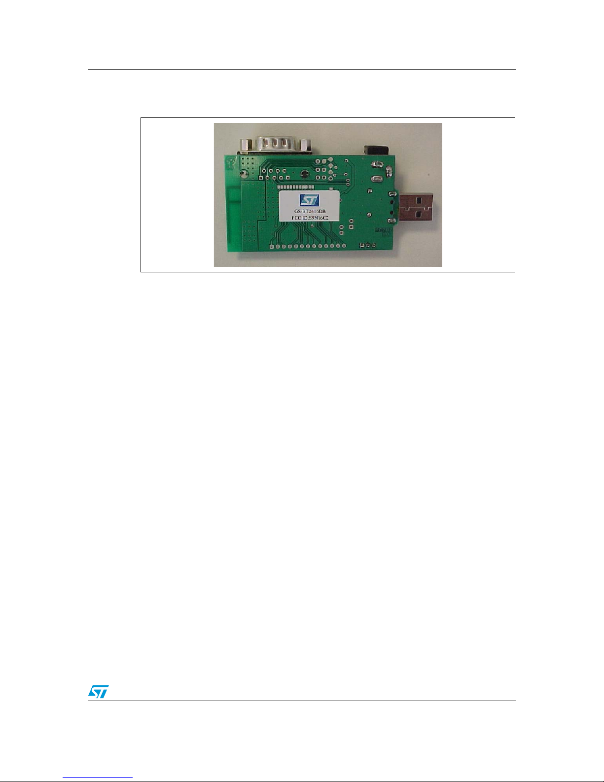
This board has the following FCC ID: S9N16C2.
Figure 5. FCC ID position
6.2.1 FCC Statement
This device complies with Part 15 of the FCC Rules. Operation is subject to the following two
conditions:
1. this device may not cause harmful interference, and
2. this device must accept any interference received, including interference that may
cause undesired operation.
Note: This equipment has been tested and found to comply with the limits for a Class B digital
device, pursuant to Part 15 of the FCC Rules. These limits are designed to provide
reasonable protection against harmful interference in a residential installation. This
equipment generates, uses and can radiate radio frequency energy and, if not installed and
used in accordance with the instructions, may cause harmful interference to radio
communications.
However, there is no guarantee that interference will not occur in a particular installation.
If this equipment does cause harmful interference to radio or television reception, which can
be determined by turning the equipment off and on, the user is encouraged to try to correct
the interference by one or more of the following measures:
– Reorient or relocate the receiving antenna
– Increase the distance between the equipment and receiver
– Connect the equipment to an outlet on a circuit different from that to which the
receiver is connected
Consult the dealer or an experienced radio/TV technician for help.
●Antenna
Our board type GS-BT2416C2DB.xxx is for OEM integrations only. The end-user product
will be professionally installed in such a manner that only the authorized antennas are used.
●Caution
Any changes or modifications not expressly approved by the party responsible for
compliance could cause the module to cease to comply with FCC rules part 15, and thus
void the user's authority to operate the equipment.

Obsolete Product(s) - Obsolete Product(s)
Certifications UM0472
10/19
6.2.2 Label instructions
●Module type: Bluetooth class 2 board GS-BT2416C2DB.xxx (GS-BT2416C2.H or
GS-BT2416C2.AT1 module + PC 787 carrier board)
●FCC-ID: S9N16C2
The purpose of this section is to inform you how to specify the FCC ID of our Bluetooth
board GS-BT2416C2DB.xxx on your final product.
Based on the Public Notice from the FCC, the product in which the our transmitter module is
installed must display a label referring to the enclosed module.
The label should use wording such as "Contains Transmitter module FCC ID: S9N16C2” or
"Contains FCC ID: S9N16C2”. Any similar wording that expresses the same meaning may
be used (see Figure 6 below for an example).
Figure 6. FCC ID label
Contains FCC ID:
S9N16C2

Obsolete Product(s) - Obsolete Product(s)
UM0472 Special requirements for modular application
11/19
7 Special requirements for modular application
The modular transmitter fulfills the following requirements:
1. The modular transmitter must have its own RF shielding:
– The RF module fulfills the emission requirements of the FCC rules without
additional shielding.
2. The modular transmitter must have buffered modulation/data inputs:
– The module has a memory management unit inside of the IC. The processor
interfaces with the external application by means of a general purpose I/O (GPIO),
Uart, USB, PCM, I2C, SPI. The processor also interfaces the RF part of the
module exchanging data and commands with it. Inside the processor flash
memory is available to download the customer application and the Bluetooth
profiles.
3. The modular transmitter must have its own power supply regulation:
– The module contains its own voltage regulation. In the event of changes in the
supply voltage VCC (for example caused by temperature changes or other
effects), the internal voltage will be stabilized.
4. The modular transmitter must comply with the antenna requirements of Section 15.203
and 15.204:
– The RF module is for OEM (Original Equipment Manufacturer) integration only.
The end-user product will be professionally installed in such a manner that only
the authorized antenna is used.
5. The modular transmitter must be tested in a stand-alone configuration:
– The RF module was tested in a stand-alone configuration.
6. The modular transmitter must be labelled with its own FCC ID number:
– The RF module will be labelled with its own FCC ID number. When the module is
installed inside the end-product, the label is not visible. The OEM manufacturer is
instructed how to apply the exterior label.
7. The modular transmitter must comply with any specific rule or operating requirements
applicable to the transmitter and the manufacturer must provide adequate instructions
along with the module to explain any such requirements:
– The EUT is compliant with all applicable FCC rules. Detailed instructions are given
in the product Users Guide.
8. The modular transmitter must comply with any applicable RF exposure requirements.
– Maximum measured power output: 1,08 mW (0,33 dBm)
– Maximum antenna gain: 1 dBi = numeric gain 1,259 (see also FCC test report)
Maximum permissible exposure defined in 47 CFR 1.1310: 1 mW/cm².
The RF module operates at low power level so it does not exceed the Commission's RF
exposure guidelines limits. Furthermore, Spread spectrum transmitters operating according
to the Section 15.247 are categorically excluded from routine environmental evaluation.

Obsolete Product(s) - Obsolete Product(s)
AT commands appendix UM0472
12/19
8 AT commands appendix
T h i s s e c t i o n i s a p p l i c a b l e t o t h e e v a l u a t i o n b o a r d w i t h t h e AT c o m m a n d d o w n l o a d e d F W
GS-BT2416C2DBAT1.
The purpose of this section is to describe all the necessary steps to establish a connection
between two Bluetooth GS-BT2416C2DBAT1 evaluation boards in a Serial line /Cable
replacement application.
(This connection example is also given in the GS-BT2416C2.AT1 datasheet, Appendix A)
8.1 Setup & connect
Two PCs and two GS-BT2416C2DBAT1 boards are needed to perform the connection.
Figure 7. Basic setup

Obsolete Product(s) - Obsolete Product(s)
UM0472 AT commands appendix
13/19
8.2 Steps to connect
(Please refer to the GS-BT2416C2.AT1 datasheet Appendix A, for the meaning of the AT
commands).
●Designate a GS-BT2416C2DBAT1 board to be used as "Client" and it has the address
0080E1000001. Hereafter this board will be referred to as "Client"
●Designate a GS-BT2416C2DBAT1 board to be used as "Server" and suppose it has
the address 0080E1000002. Hereafter this board will be referred to as "Server"
●Connect the Server board to a PC using an RS232 cable
●Connect the Client board to a PC by using an RS232 cable
●Open the HyperTerminal program on both PCs and set the communication line with the
following parameters:
– Select the proper COM line ( COM1, COM2……)
– baud rate: 9600 (default baud rate of GS-BT2416C2.AT1 module)
– data bits: 8
– parity: none
– stop bits: 1
– flow control: none
– In ASCII setup, set flag line ends with line feed
– In ASCII setup, set flag echo characters typed locally
●Power the Client board with the external 5 V: on the PC screen connected to the Client
should appear +READY
●Power the Server board with the external 5 V: on the PC screen connected to the
Server should appear +READY
●Configure the Client board using the following commands in Ta b l e 4 : (GPIO3 Client
must be Low to select Command Mode - S2 switch in Command mode)
Table 4. Client setup
Command Answer Notes
AT OK Check module ready
AT + B T C M O D E = 0 O K
AT+BTPMODE=1 OK
AT+BTDMODE=0 OK Not discoverable
AT+BTSECMODE=1 OK
AT+BTENCMODE=0 OK
AT+BTNAME=”SPP Client” OK Set client name

Obsolete Product(s) - Obsolete Product(s)
AT commands appendix UM0472
14/19
●Configure the Server board using the following commands in Ta b l e 5 : (GPIO3 Server
must be Low to select Command Mode- S2 switch in Command mode)
After the configuration of the Server board, GPIO3 must be put HIGH to select DATA MODE
which enables the Server board to receive and transmit DATA.
●Inquiry & available services
Before establishing a connection, the Client has to know which Bluetooth devices are
present and which services are offered, and therefore the Client:
– first performs the inquiry by the command:
AT+BTINQ=xx
where xx is the inquiry time (i.e. 10 sec -> AT+BTINQ=10).
The answer is a list of present Bluetooth connectable devices. One of the devices
should be our SPP Server:
+BTINQRES:0080E1000002,"SPP Server"
OK
– then asks which kind of service is available with the command:
AT+BTRPORTS=0080E1000002
The a nswe r is:
+BTRPORT:"SPP Port",1
s e r i a l p o r t p r o f i l e , p o r t 1 ( c a n b e 1 , 2 … )
OK
●Once the Client knows the device present and the service offered, the Client finalizes
the connection with the command:
AT + B T C O N N E C T = 0 0 8 0 E 10 0 0 0 0 2 , 1 , " 1 2 3 4 ", 1 , 0
OK
At this point the connection is established and GPIO1 (indicating the connection status) on
both Client and Server boards becomes high.
On the GS-BT2416C2DBAT1 board an LED is connected to GPIO1 and therefore the
connection is also shown by an LED on.
GPIO3 on the Client board must be now put at HIGH level allowing the Client to send and
receive DATA from the Server.
Table 5. Server setup
Command Answer Notes
AT OK Check module ready
AT + B T C M O D E = 1 O K
AT+BTPMODE=1 OK
AT+BTDMODE=1 OK Discoverable
AT+BTSECMODE=1 OK
AT+BTENCMODE=0 OK
AT+BTPINCODE=”1234” OK Pin code
AT+BTNAME=”SPP Server” OK Set server name
AT+BTCLASS=52020C OK
AT+BTREGPORT=”SPP port” OK Name of service offered

Obsolete Product(s) - Obsolete Product(s)
UM0472 AT commands appendix
15/19
●Disconnection
To disconnect, the Client has to put its GPIO3 LOW (Command mode) (changing from high
t o l o w o n G P I O 3 a p p e a r s o n t h e C l i e n t P C s c r e e n a s + R E A D Y ) a n d s e n d s t h e c o m m a n d :
AT+BTDISCONNECT
OK
The result is the disconnection of the link Client / Server, and GPIO1 on both Client and
Server boards returns to low (the LEDs go off).
8.3 Macro instructions
The MACRO concept with the commands AT+BTMACROSTART, AT+BTMACROSTOP and
AT+MACROCLEAR has been introduced with version 1.2.1.8 of AT1 SW.
These commands work in such a way that all commands written between the
AT+BTMACROSTART and AT+BTMACROSTOP commands are stored inside the internal
flash memory and executed at each power up of the module.
Note: When you insert a command between MACROSTART and MACROSTOP you do not have
immediate execution of the command but only storing in flash memory. The module
answers with OK or ERROR from a syntax point of view. Execution is active at the next
power on.
After writing the commands between the two macro commands, the module could work in
stand-alone without needing to program it at each power on.
The MACROCLEAR command erases all commands stored.
As an example: suppose the previous modules always have the final address 01 (Client)
and 02 (Server) and we already know which connection to get.
Write the following sequence of commands in Client and Server module (see Tabl e 6). After
the MACROSTOP command, they are stored in the internal memory of the corresponding
module.
Table 6. Macro example
Client Server
AT+BTMACROSTART AT+BTMACROSTART
AT + B T C M O D E = 0 AT + B T C M O D E = 1
AT+BTPMODE=1 AT+BTPMODE=1
AT + B T D M O D E = 0 AT + B T D M O D E = 1
AT+BTSECMODE=1 AT+BTSECMODE=1
AT+BTENCMODE=0 AT+BTENCMODE=0
AT+BTNAME="SPP Client" AT+BTPINCODE="1234"
AT+BTCLASS=52020C AT+BTNAME="SPP Server"
AT+BTCONNECT=0080E1000002,1,"1234",10,5 AT+BTCLASS=52020C
AT+BTMACROSTOP AT+BTREGPORT="SPP port"
AT + B T M AC R O S TO P

Obsolete Product(s) - Obsolete Product(s)
AT commands appendix UM0472
16/19
Note that:
●When the address module to connect to is known, the inquiry command can be omitted
●The BTCONNECT command has been set to 10 retries at 5 sec intervals.
After the modules have been programmed, you can power off and power on again the
modules themselves. At a certain point the modules will be connected to each other (LED
on) without any intervention.
The sequence of powering on does not matter. The only rule to follow is that, once the
Client has been powered on, the Server must be powered in the time set by the 10 retries at
5 sec interval.
During the macro execution the module answers with "OK” or "ERROR" for each command
executed. This feedback can be eliminated using the AT+ECHO=OFF command.
8.4 Module BT address
Each module has its own address which identifies the module itself in the network. The
above examples were used with addresses 0080E1000001 and 0080E1000002.
Modules on the GS-BT2416C2DBAT1 board could have different addresses. Before starting
to send commands, the module address can be found with the command
AT+BTSETTINGS=? which shows the relevant information of the module including the BT
address.

Obsolete Product(s) - Obsolete Product(s)
UM0472 AT commands appendix
17/19
8.5 Point-to-point connection
Modules with AT commands firmware can only perform point-to-point connections. Only one
connection can be activated at once.
A module can be connected to several other modules, but it has to disconnect from the
previous connection before activating a new one.
Figure 8 shows an example of a Client C1 which needs to connect to Server S1,S2,..Sn:
In this case the following procedure must be used:
●C1 establishes the connection to S1 to exchange data
●C1 disconnects from S1 using the command AT+BTDISCONNECT
●C1 establishes the connection to S2 to exchange data
●C1 disconnects from S2 using the command AT+BTDISCONNECT
●C1 establishes the connection to Sn to exchange data… and so on.
Figure 8. Point-to-point connection
C1
S1
S2
Sn

Obsolete Product(s) - Obsolete Product(s)
Revision history UM0472
18/19
9 Revision history
Table 7. Document revision history
Date Revision Changes
22-Oct-2007 1 Initial release

Obsolete Product(s) - Obsolete Product(s)
UM0472
19/19
Please Read Carefully:
Information in this document is provided solely in connection with ST products. STMicroelectronics NV and its subsidiaries (“ST”) reserve the
right to make changes, corrections, modifications or improvements, to this document, and the products and services described herein at any
time, without notice.
All ST products are sold pursuant to ST’s terms and conditions of sale.
Purchasers are solely responsible for the choice, selection and use of the ST products and services described herein, and ST assumes no
liability whatsoever relating to the choice, selection or use of the ST products and services described herein.
No license, express or implied, by estoppel or otherwise, to any intellectual property rights is granted under this document. If any part of this
document refers to any third party products or services it shall not be deemed a license grant by ST for the use of such third party products
or services, or any intellectual property contained therein or considered as a warranty covering the use in any manner whatsoever of such
third party products or services or any intellectual property contained therein.
UNLESS OTHERWISE SET FORTH IN ST’S TERMS AND CONDITIONS OF SALE ST DISCLAIMS ANY EXPRESS OR IMPLIED
WARRANTY WITH RESPECT TO THE USE AND/OR SALE OF ST PRODUCTS INCLUDING WITHOUT LIMITATION IMPLIED
WARRANTIES OF MERCHANTABILITY, FITNESS FOR A PARTICULAR PURPOSE (AND THEIR EQUIVALENTS UNDER THE LAWS
OF ANY JURISDICTION), OR INFRINGEMENT OF ANY PATENT, COPYRIGHT OR OTHER INTELLECTUAL PROPERTY RIGHT.
UNLESS EXPRESSLY APPROVED IN WRITING BY AN AUTHORIZED ST REPRESENTATIVE, ST PRODUCTS ARE NOT
RECOMMENDED, AUTHORIZED OR WARRANTED FOR USE IN MILITARY, AIR CRAFT, SPACE, LIFE SAVING, OR LIFE SUSTAINING
APPLICATIONS, NOR IN PRODUCTS OR SYSTEMS WHERE FAILURE OR MALFUNCTION MAY RESULT IN PERSONAL INJURY,
DEATH, OR SEVERE PROPERTY OR ENVIRONMENTAL DAMAGE. ST PRODUCTS WHICH ARE NOT SPECIFIED AS "AUTOMOTIVE
GRADE" MAY ONLY BE USED IN AUTOMOTIVE APPLICATIONS AT USER’S OWN RISK.
Resale of ST products with provisions different from the statements and/or technical features set forth in this document shall immediately void
any warranty granted by ST for the ST product or service described herein and shall not create or extend in any manner whatsoever, any
liability of ST.
ST and the ST logo are trademarks or registered trademarks of ST in various countries.
Information in this document supersedes and replaces all information previously supplied.
The ST logo is a registered trademark of STMicroelectronics. All other names are the property of their respective owners.
© 2007 STMicroelectronics - All rights reserved
STMicroelectronics group of companies
Australia - Belgium - Brazil - Canada - China - Czech Republic - Finland - France - Germany - Hong Kong - India - Israel - Italy - Japan -
Malaysia - Malta - Morocco - Singapore - Spain - Sweden - Switzerland - United Kingdom - United States of America
www.st.com
This manual suits for next models
1
Table of contents
Other ST Motherboard manuals

ST
ST STEVAL-IPC002V1 User manual

ST
ST STM32G4 Nucleo-64 User manual

ST
ST STM32L4R9I-EVAL User manual

ST
ST STCC50x1 User manual

ST
ST EVAL-L99DZ200 User manual

ST
ST EVALKITSTKNX User manual

ST
ST M24SR-DISCOVERY User manual

ST
ST STM3240G-EVAL User manual

ST
ST STM32429I-EVAL1 User manual

ST
ST STEVAL-IDB007V Series User manual