Page 4
POWERING TECHNOLOGY
Manual No. sli-15-5 sli15-man-rev5-0718.indd
FIGURES
Figure 1-1 Input Current Absorption .............................................................................................................5
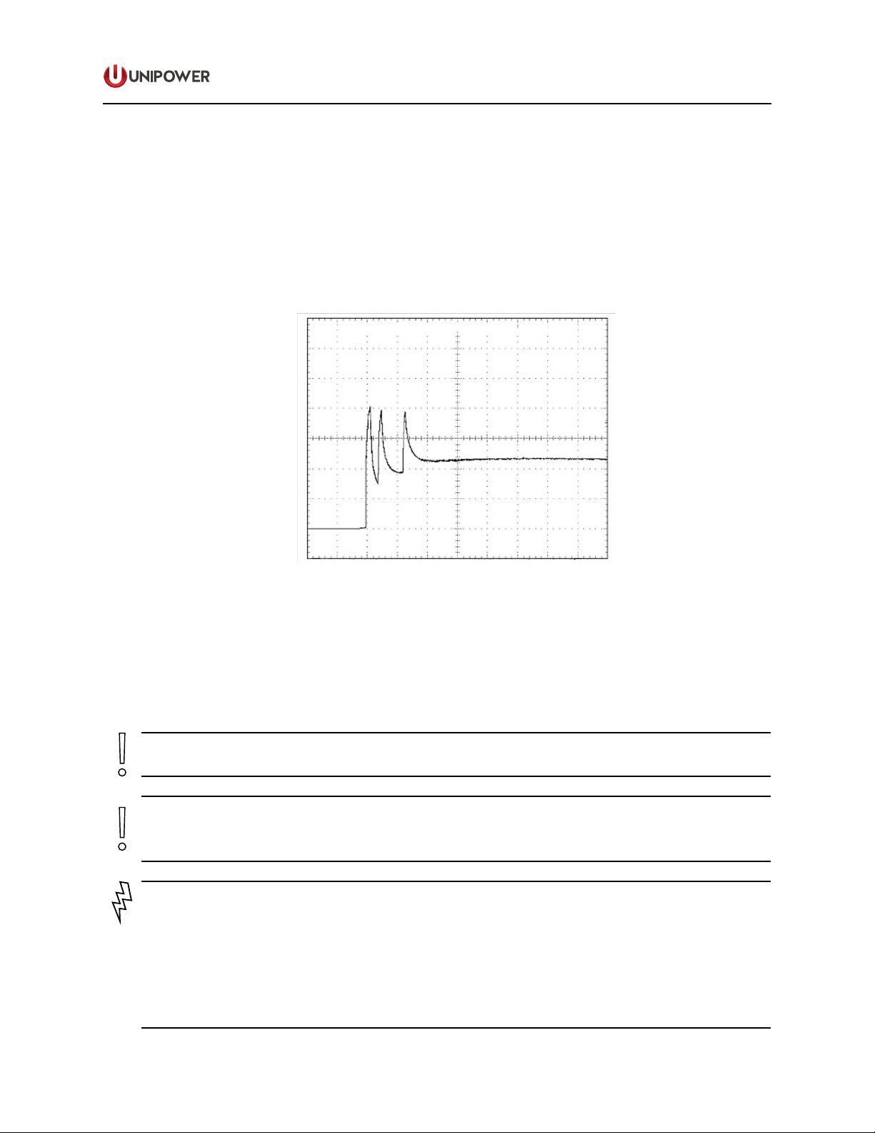
Figure 1-2 Input Breaker Delay .....................................................................................................................6
Figure 4-1 Fitting Mounting Brackets .........................................................................................................10
Figure 4-2 Mounting Dimensions................................................................................................................11
Figure 4-3 Rear View...................................................................................................................................11
Figure 4-4 Input Connection Bus Bars ........................................................................................................11
Figure 4-5 DC Input Clips in sub-rack ........................................................................................................12
Figure 4-6 Plug Connections .......................................................................................................................12
Figure 4-7 Screw Terminal Connections .....................................................................................................12
Figure 4-8 AC Output Connections for n-inverters in parallel conguration - plug connectors .................13
Figure 4-9 AC Output Connections for n-inverters in parallel conguration - screw terminals .................13
Figure 4-10 AC grid input connections for parallel conguration - plug connectors..................................14
Figure 4-11 AC grid input connections for parallel conguration - screw terminals ..................................14
Figure 4-12 Signal Connector Type .............................................................................................................15
Figure 4-13 Parallel Conguration Signal Connections ..............................................................................16
Figure 4-14 Parallel Adapter for Standalone Units......................................................................................17
Figure 4-15 Parallel Adapter for Hot-Plug Units.........................................................................................18
Figure 4-16 Signal Connections for 3-phase Y Output Conguration.........................................................19
Figure 5-1 Front Panel Display/Touch Pad..................................................................................................27
Figure 5-2 Startup and Status Menu ............................................................................................................29
Figure 5-3 Main Menu Structure .................................................................................................................30
Figure 5-4 Settings Menu Navigation..........................................................................................................32
Figure 5-5 Settings Menu Structure.............................................................................................................33
Figure 5-6 Protections Sub-menu Structure.................................................................................................36
Figure 5-7 Transfer Switch Sub-menu Structure .........................................................................................37
Figure 5-8 STS Voltage Mask......................................................................................................................38
Figure 5-9 STATUS Menu ...........................................................................................................................40
Figure 5-10 INFO Menu ..............................................................................................................................41
Figure B-1 Manual Bypass Scematic...........................................................................................................44
Figure C-1 Grounding of Neutral for Inverters with Transfer Switch .........................................................46
Figure C-1 SERVICE sub-menu structure ...................................................................................................47
Figure F-1 SLI to ACX Translator Connectors............................................................................................51
Figure F-2 Typical System Schematic .........................................................................................................53
TABLES
Table 4-1 Signal Description .......................................................................................................................15
Table 5-1 Front Panel LED Status Indications ............................................................................................28
Table A-1 Input Requirements .....................................................................................................................43
Table A-2 Input Wire Size............................................................................................................................43
Table C-1 Grounding Restrictions ...............................................................................................................46
Table E-1 Factory Settings...........................................................................................................................49
Table F-1 SLI to ACX Translator Signal Connections ................................................................................51
Table F-2 SLI to ACX Translator Power Connections ................................................................................52