Wavelength Electronics PLD K-CH Series User manual
ORDERING INFORMATION
PART NO DESCRIPTION
PLD5K-CH 5 A Laser Diode Driver
PLD10K-CH 10 A Laser Diode Driver
PLD12.5K-CH 12.5 A Laser Diode Driver
WCB308 Power / LD Cable Set
RELIABILITY YOU CAN TRUST
The PLDxK-CH Series Laser Diode Drivers deliver the
reliability and performance you expect from a Wavelength
Electronics laser driver in a compact and easy-to-integrate
package.
APPLICATIONS
Tens of thousands of PLD drivers are deployed in particle
counters, manufacturing vision systems, wavefront
beyond doubt the reliability and stability of the design.
DESIGNED FOR EASY INTEGRATION
The PLDxK-CH drivers operate from a single 5 V power
supply. To accommodate high compliance lasers, or
multiple stacked lasers, the PLDxK-CH laser diode drivers
allow the laser to be driven from a separate power supply
up to 30 V.
LASER SAFETY FEATURES
Built-in safety features make your product more robust
to real world operating conditions: latching current limit
shorting relay protects the laser from ESD events.
Long-term reliability means better up-time, fewer service
products.
FEATURES AND BENEFITS
• Models: 5 A, 10 A, 12.5 A
• 5 A and 10 A models operate from a single 5 VDC
• Separate power supply can be used to drive
high-compliance lasers up to 28 V
• Product Variation allows high-compliance up to
85 V.
• Constant Current or Constant Power modes
• Safety features protect your laser
»Adjustable latching current limit
»Slow-start circuitry
• Local and Remote Enable controls
CONTENTS
QUICK CONNECT GUIDE 2
PIN DESCRIPTIONS 4
ELECTRICAL SPECIFICATIONS 6
SAFETY INFORMATION 7
OPERATING INSTRUCTIONS 8
ADDITIONAL TECHNICAL INFORMATION 15
TROUBLESHOOTING 21
MECHANICAL SPECIFICATIONS 23
CERTIFICATION AND WARRANTY 24
e
PAGE
Pb
RoHS
Compliant
Applies to Product Revisions
PLD5K-CH & PLD10K-CH: Rev A – D
PLD12.5K-CH: Rev A – B
© April 2020
406-587-4910
www.teamWavelength.com
PLDxK-CH Series
Chassis Mount Laser Diode Drivers
DATASHEET AND OPERATING GUIDE
© 2020 www.teamWavelength.com 2
PLDXK-CH SERIES LASER DIODE DRIVER
QUICK CONNECT GUIDE
!
Visit the Wavelength Electronics website for the most
www.teamwavelength.com/support/design-tools/soa-ld-calculator/
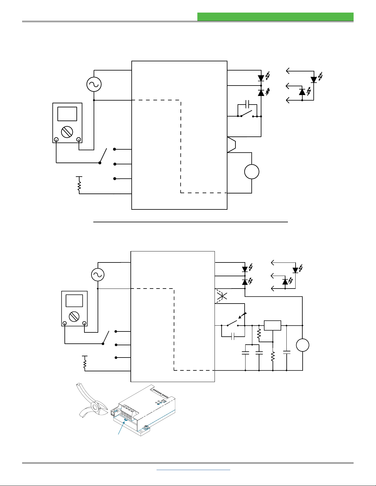
Figure 1 shows the top view of the PLDxK-CH driver and
Current Limit adjust trimpots, and pins.
Figure 2 shows a typical wiring diagram for the PLDxK-CH
driver to operate a Type A or B laser. Refer to Table 3 on
page 8 for additional wiring diagrams, or if you are using
the PLD12.5K-CH.
Figure 3 illustrates the three laser types that the PLDxK-CH
laser types refer to the Operating Instructions.
Figure 1. PLDxK-CH Driver Controls
* DO NOT change switch positions while the output
is enabled; Doing so may damage the laser diode.
!
H1
J1
PDC
PDA
PLD K-CH
LIM I ADJ - I DISABLED
OUT ADJ - OUT ENABLED
LASER DIODE DRIVER
CP/CC
PD - Lo/Hi
LDC
LDA
+5V
GND
Setpoint Adjust (12-turn) Operating Mode *
PD Range *
L = 15 – 500 µA
H = 50 – 5000 µA
CP = Constant Power
CC = Constant Current
J1
J3
J2
Limit Adjust (12-turn)
Current Limit LED
Output Enabled LED
H1
PIN 1: COMMON
Photodiode Output (PD OUT - type C lasers only)
Enabled Status (LD STATUS)
Output Enable (LD ENABLE)
Modulation Input (ANALOG IN)
Photodiode Voltage (PDV - type C lasers only)
PIN 1: COMMON
Limit Current Monitor (LMON)
Photodiode Current Monitor (PMON)
Current Monitor (IMON)
J3:4
H1:4 OR
LD Anode
LD Cathode
H1:2
H1:3
LD Enable Closed = Output Enabled
Open = Output Disabled
H1:1
+5 V
GND
(Internally Shorted)
J3:5
J3:1
or
J2:1
J2:4
J3:3
J2:3
J2:2
Analog Input
P Monitor
(PD Current)
I Monitor
(Output Current)
LIM I Monitor
LIM I Status
Optional External
Setpoint (0 to 5 V)
+
-
5 VDC
PD Anode J1:1
0.1 µF
Common
(Low Current)
+5V
10 kΩ
Pull Up Resistor
Short J3:5 to J3:1 when
analog input is not used.
PD
LD
PD
LD
* The External Jumper is installed only on the
PLD5K-CH and PLD10K-CH. The External
Jumper is not installed on the PLD12.5K-CH.
DMM
Jumper *
+
-
* A twisted-pair Power and LD Cable
is available separately (WCB308)
Figure 2. Quick Connect Wiring Diagram, Type A & B Laser Diodes
Type A Laser Diode Type B Laser Diode Type C Laser Diode
Common
Cathode
Laser Diode Anode &
Photodiode Cathode Common Isolated Photodiode
Short the
Laser Diode Anode
to Photodiode Cathode
Common
Anode
Laser Diode Cathode &
Photodiode Anode Common
Figure 3. Laser Type Diagrams

© 2020 www.teamWavelength.com 3
PLDXK-CH SERIES LASER DIODE DRIVER
QUICK CONNECT GUIDE, CONTINUED
refer to Figure 4. When using the test load, the actual drive
current can be determined by measuring the voltage drop
across the resistor. Do not place an ammeter in series with
the load circuit.
1.5 - 2.5 V Compliance,
Current to 15.0 A,
Components must
be heat-sinked.
0.05 Ω
100 W
STPS20M100ST (2x)
J3:4
H1:4
LD Anode
LD Cathode
H1:3
LD Enable
0.1 µF
Figure 4. Constant Current Mode Laser Test Loads
REVISION MARKING
The product revision is marked in the third place of the serial
number stamped on the cover. For example, CHA0852111
is a Revision A driver.
© 2020 www.teamWavelength.com 4
PLDXK-CH SERIES LASER DIODE DRIVER
PIN DESCRIPTIONS
Table 1. Pin Descriptions
PIN NAME CABLE
COLOR PIN DESCRIPTION
1 GND Black Power Supply Ground. High current return for the +5 V power supply input.
2 +5 V Red
Supply voltage to control electronics. Also used to power the laser diode on the
PLD5K-CH and PLD10K-CH. This pin is tied to Pin H1:3 by factory-installed
high-compliance lasers. The PLD12.5K-CH is delivered from the factory with the
PLD12.5K-CH. See Figure 6 on page 9.
3 LDA White
Laser Diode Anode. This pin is tied to Pin H1:2 by factory-installed external jumper on
Figure 6 on
page 9.
4 LDC Blue Laser Diode Cathode.
1 PDA Red Photodiode Anode for Type A and Type B lasers.
See Figure 7 and Figure 10 for operation with Type C laser diode packages.
2 PDC Black
See Figure 7 and Figure 10.
1 Black
2 White
Current Limit Setpoint Monitor. Transfer function varies by model—refer to Table 2.
3 Red
setting—refer to Table 2
4 Green Table 2.
1 Black
2
See Figure 7 and Figure 10.
3 WHite
high impedance during normal operation. Toggle LD Enable to reset the limit circuit and
enable the output current.
4 LD ENABLE Red
5 Green
Remote setpoint or modulation input. Transfer function varies by model and operating
mode—refer to Table 2
Electrical Specications for damage threshold information.
6 PDV Blue Photodiode Voltage. For Type C laser diode packages only.
See Figure 7 and Figure 10.
Figure 17 on page 16.

© 2020 www.teamWavelength.com 5
PLDXK-CH SERIES LASER DIODE DRIVER
Table 2. Current Output Monitor, Limit Monitor, Photodiode Current Monitor, and
Analog Input Transfer Functions
FUNCTION MODE LABEL PLD5K-CH PLD10K-CH PLD12.5K-CH
CC / CP V 2 A / V 4.6 A / V 5 A / V
CC / CP V 2 A / V 4.6 A / V 5 A / V
CC 1 A / V 2.3 A / V 2.5 A / V
Low Range CC / CP V 200 µA / V
High Range See Note CC / CP V 2 mA / V
Low Range CP 100 µA / V
High Range See Note CP 1 mA / V
Note: High Range is not available when using Type C Lasers.

© 2020 www.teamWavelength.com 6
PLDXK-CH SERIES LASER DIODE DRIVER
ELECTRICAL SPECIFICATIONS
PARAMETER SYMBOL VALUE UNIT NOTE
ABSOLUTE MAXIMUM RATINGS
+5 V 5.0 to 5.5 VDC page 8
1
PLD12.5K-CH laser supply
High Compliance laser
LD Anode 4.5 to 30 VDC
voltages > 5 VDC, see page 20
page 8.
Supply Voltage, Type C Lasers1Aux V+ 8.0 to 12.5 VDC
2T 0 to 50 ºC
Storage Temperature Range TSTG -55 to 125 ºC
Weight 3.2 oz 89.6 g
Size 1.12 x 2.35 x 3.2 in 28.5 mm x 59.7 mm x 81.3 mm
2. Maximum operating temperature of PLD12.5K-CH is 35ºC.
MODEL
PARAMETER PLD5K-CH PLD10K-CH PLD12.5K-CH UNIT NOTE
DRIVE CURRENT OUTPUT
40 W
5110112.51A
Compliance Voltage2
3 V max with 5 V power supply input
28 V max with 30 V power supply input
85 V max with Product Variation
V
Short Term Stability, 1 hour < 100 < 200 < 200 ppm
Quiescent Current 150 150 250 mA
< 200 ppm / ºC
Noise & Ripple3> 45 µA
PHOTODIODE FEEDBACK
50 - 5000 µA
Low Range 15 - 500 µA
Constant Power Mode
< 0.02 < 0.05 < 0.05 %
EXTERNAL MODULATION
V
1
3 dB Bandwidth, Constant Current4120 80 50 kHz
BW at 90% Depth of Modulation470 70 40 kHz Constant Current Mode
4.8 / 9.4 5.9 / 10 8 / 9 µsec
TIMING CHARACTERISTICS
seconds
250 msec
Disable Fall Time >100 µsec
MONITOR ACCURACY
based on transfer function 2% of Full
Scale
1. To achieve maximum rated current, the power supply voltage may need to be 5.5 VDC because the impedance of external wiring may reduce
the voltage at the laser driver.
mode, a maximum compliance voltage of 28 V is obtained using a 30 VDC
power supply. A 5 VDC power supply input results in 3 V compliance voltage.
3. Not recommend for low noise applications. See the LDxCHA webpage for lower noise laser drivers
4.
0 mA
Full Current
100% Depth of Modulation at 10 Hz
100 %
0 %
90% Depth of Modulation at 70 kHz
90 %
95 %
5 %

© 2020 www.teamWavelength.com 7
PLDXK-CH SERIES LASER DIODE DRIVER
SAFETY INFORMATION
SAFE OPERATING AREA — DO NOT EXCEED
INTERNAL POWER DISSIPATION LIMITS
Before attempting to operate the PLDxK-CH driver, it is
within the Safe Operating Area
To determine if the PLDxK-CH driver is suitable for your
application and if it will be operating in the safe range,
Area online:
www.teamwavelength.com/support/design-tools/soa-ld-calculator/
(page 20
instead.
!
calculator, call the factory for free and prompt technical
assistance.
THEORY OF OPERATION
The PLDxK-CH Series drivers are controlled current
sources: they deliver the current commanded by the
setpoint. The current source continually monitors the actual
output current, compares it to the setpoint, and adjusts the
signal that represents the output current. The voltage and
output current are related by a transfer function that varies
by driver model number.
The setpoint voltage is adjusted with the onboard trimpot or
by an external input that sums with the onboard setpoint.
The adjustable current limit is set using an onboard trimpot.
As current is driven through the load, there is a voltage drop
across the load because of the impedance. As the current
increases, the voltage drop may increase to the point that it
reaches the Compliance Voltage limit of the current source.
increase the current driven to the load even if you increase
the setpoint.
The PLDxK-CH driver includes features that help protect
your laser and make the driver more versatile in a wide
array of applications:
• The user-adjustable latching current limit protects the
output when a limit condition is detected. Toggling the
Enable resets the current limit circuit.
•
seconds from the time the Enable signal is applied.
•
250 msec.
© 2020 www.teamWavelength.com 8
PLDXK-CH SERIES LASER DIODE DRIVER
OPERATING INSTRUCTIONS
according to the actual application.
We recommend using a test load until you are familiar with
operation of the driver. Refer to page 3 for test load
schematics.
NECESSARY EQUIPMENT
• PLDxK-CH controller
• Digital voltmeter, 4-½ digit resolution recommended
•
• Laser diode, mount, and optional temperature control
system
• Connecting wires
•
POWER SUPPLY REQUIREMENTS
Linear-regulated or low-noise switching power supplies can
be used. We recommend using power supplies with noise
For single-supply operation, PLD5K-CH and PLD10K-CH:
• 5 VDC power supply rated for 1.1-times the maximum
laser diode current, plus 150 – 250 mA for the electronics
(see Electrical Specications
For Type C lasers with the PLD5K-CH and PLD10K-CH:
• 8 to 12 VDC power supply rated for 250 mA, plus
Figure 7 and
Figure 10
•
power supply for the laser, rated for 1.1-times the
maximum laser diode current
For two-supply operation when using the PLD5K-CH or
PLD10K-CH to drive a high-compliance laser, laser bar, or
• 5 VDC power supply rated for 250 mA for electronics
•
1.1-times the maximum laser diode drive current and
> 2 V greater than the compliance voltage of the laser
NOTE: It is critical to shut down the power supply to
the laser rst before shutting down the +5V supply
powering the electronics. Failure to follow this order
may damage the PLD or laser.
SAFE OPERATING AREA AND
THERMAL DESIGN CONSIDERATIONS
but we recommend you use the online tools instead.
www.teamwavelength.com/support/design-tools/soa-ld-calculator/
!
PREVENT DAMAGE FROM ELECTROSTATIC
DISCHARGE
Before proceeding, it is critical that you take precautions to
and your laser. ESD damage can result from improper
handling of sensitive electronics, and is easily preventable
with simple precautions.
Enter the search phrase “ESD Precautions for Handling
Electronics
on ESD-safe handling practices.
We recommend that you always observe ESD precautions
when handling the PLDxK-CH driver and your laser diode.
Note: The PLDxK-CH case is isolated from electrical ground.
WIRE THE PLDxK-CH LASER DRIVER
Refer to Table 3
(see Figure 4
Table 3. Wiring Congurations
PRODUCT CONFIGURATION DIAGRAM
PLD5K-CH
PLD10K-CH
Type A & B Laser Diode,
Single 5 VDC Power Supply Figure 5
Type A & B Laser Diode,
High-Compliance Laser Figure 6
Type C Laser Diode,
Single Power Supply Figure 7
Type A & B Laser Diode,
Negative Power Supply or
Grounded Laser Anode
Figure 8
PLD12.5K-CH
Type A & B Laser Diode Figure 9
Type C Laser Diode Figure 10
Type A & B Laser Diode,
Negative Power Supply or
Grounded Laser Anode
Figure 11
© 2020 www.teamWavelength.com 9
PLDXK-CH SERIES LASER DIODE DRIVER
WIRING THE PLD5K-CH AND PLD10K-CH
Figure 5. Type A & B Laser Diode, Single 5 VDC Power Supply
PLD5K-CH and PLD10K-CH
J3:4
H1:4 OR
LD Anode
LD Cathode
H1:2
H1:3
LD Enable Closed = Output Enabled
Open = Output Disabled
H1:1
+5 V
GND
(Internally Shorted)
J3:5
J3:1
or
J2:1
J2:4
J3:3
J2:3
J2:2
Analog Input
P Monitor
(PD Current)
I Monitor
(Output Current)
LIM I Monitor
LIM I Status
Optional External
Setpoint (0 to 5 V)
+
-
5 VDC
PD Anode J1:1
0.1 µF
Common
(Low Current)
+5V
10 kΩ
Pull Up Resistor
Short J3:5 to J3:1 when
analog input is not used.
PD
LD
PD
LD
* The External Jumper is installed only on the
PLD5K-CH and PLD10K-CH. The External
Jumper is not installed on the PLD12.5K-CH.
DMM
Jumper *
+
-
* A twisted-pair Power and LD Cable
is available separately (WCB308)
Figure 6. High-Compliance Laser Diode Operation
PLD5K-CH and PLD10K-CH
LD Anode
LD Cathode
LD Enable
+5 V
GND
(Internally Shorted)
Analog Input
LIM I Monitor
LIM I Status
+
-
PD Anode
Common
(Low Current)
PD
LD
OR
+
-
10µF 0.1µF
7 to
30 VDC
LM 317
+5V REG.
732Ω
243Ω 1
3
2
330µF
0.1µF
This circuit shows how to use a single power supply.
The LM317 (+5 V Regulator) circuit can be replaced
with a separate 5 VDC power supply.
PD
LD
+5V
10 kΩ
Pull Up Resistor
DMM
P Monitor
(PD Current)
I Monitor
(Output Current)
Optional External
Setpoint (0 to 5 V)
Short J3:5 to J3:1 when
analog input is not used. J3:5
J3:1
or
J2:1
J2:4
J3:3
J2:3
J2:2
Jumper *
J3:4
H1:4
H1:2
H1:3
H1:1
J1:1
* Jumper Configuration for High-Compliance Operation:
- PLD5K-CH and PLD10K-CH: cut the jumper connecting H1:2 to H1:3.
- PLD12.5K-CH: the jumper is removed at the factory; two power supplies
are required to operate the PLD12.5K-CH.
* A twisted-pair Power and LD Cable
is available separately (WCB308)
Closed = Output Enabled
Open = Output Disabled
CUT JUMPER
FOR HIGH
COMPLIANCE
OPERATION
NOTE: For two-supply operation, it is critical to shut down the power supply to the laser rst before shutting down the +5V
supply powering the electronics.

© 2020 www.teamWavelength.com 10
PLDXK-CH SERIES LASER DIODE DRIVER
WIRING THE PLD5K-CH AND PLD10K-CH (CONTINUED)
Figure 7. Type C Laser Diode; PLD5K-CH and PLD10K-CH
LD Anode
LD Cathode
LD Enable
+5 V
GND
(Internally Shorted)
Analog Input
LIM I Monitor
LIM I Status
+
-
PD Cathode
Common
(Low Current)
PD
LD
OR
+
-
10µF 0.1µF
8 to
12.5 VDC
LM 317
+5V REG.
732Ω
243Ω 1
3
2
330µF
0.1µF
This circuit shows how to use a single power supply.
The LM317 (+5 V Regulator) circuit can be replaced
with a separate 5 VDC power supply.
PD
LD
+5V
10 kΩ
Pull Up Resistor
DMM
P Monitor
(PD Current)
I Monitor
(Output Current)
Optional External
Setpoint (0 to 5 V)
Short J3:5 to J3:1 when
analog input is not used. J3:5
J3:1
or
J2:1
J2:4
J3:3
J2:3
J2:2
Jumper*
J3:4
H1:4
H1:2
H1:3
H1:1
J1:2
PDV J3:6
PD
Anode
PD Aux
Out
J1:1 J3:2
* The External Jumper is installed only on the PLD5K-CH
and PLD10K-CH. The External Jumper is not installed on
the PLD12.5K-CH.
* A twisted-pair Power and LD Cable
is available separately (WCB308)
Closed = Output Enabled
Open = Output Disabled
Figure 8. Type A & B Lasers, Negative Power Supply Operation; PLD5K-CH and PLD10K-CH
J3:4
H1:4 OR
LD Anode
LD Cathode
H1:2
H1:3
LD Enable Closed = Output Enabled
Open = Output Disabled
H1:1
+5 V
GND
(Internally Shorted)
J3:5
J3:1
or
J2:1
J2:4
J3:3
J2:3
J2:2
Analog Input
P Monitor
(PD Current)
I Monitor
(Output Current)
LIM I Monitor
LIM I Status
Optional External
Setpoint (0 to 5 V)
+
-
5 VDC
PD Anode J1:1
0.1 µF
Common
(Low Current)
Short J3:5 to J3:1 when
analog input is not used.
PD
LD
PD
LD
DMM
10 kΩ
Pull Up Resistor
GND (Note 2)
+
-
Jumper (Note 1)
1. The External Jumper is installed only on the
PLD5K-CH and PLD10K-CH. The External
Jumper is not installed on the PLD12.5K-CH.
2. Isolate this ground connection from Earth if
there are any other Earth-grounded
components in the system.
* A twisted-pair Power and LD Cable
is available separately (WCB308)
NOTE: For two-supply operation, it is critical to shut down the power supply to the laser rst before shutting down the +5V
supply powering the electronics.
© 2020 www.teamWavelength.com 11
PLDXK-CH SERIES LASER DIODE DRIVER
WIRING THE PLD12.5K-CH
Figure 9. Type A & B Laser Diode, Using Two Power Supplies; PLD12.5K-CH
J3:4
H1:4 OR
LD Anode
LD Cathode
H1:2
H1:3
LD Enable Closed = Output Enabled
Open = Output Disabled
H1:1
+5 V
GND
(Internally Shorted)
J3:5
J3:1
or
J2:1
J2:4
J3:3
J2:3
J2:2
Analog Input
P Monitor
(PD Current)
I Monitor
(Output Current)
LIM I Monitor
LIM I Status
Optional External
Setpoint (0 to 5 V)
+
-
5 VDC
PD Anode J1:1
0.1 µF
Common
(Low Current)
+5V
10 kΩ
Pull Up Resistor
Short J3:5 to J3:1 when
analog input is not used.
PD
LD
PD
LD
DMM
+
-4.5 to 30 VDC
GND
+
-
* A twisted-pair Power and LD Cable
is available separately (WCB308)
Figure 10. Type C Laser Diode Operation; PLD12.5K-CH
LD Anode
LD Cathode
LD Enable
+5 V
GND
(Internally Shorted)
Analog Input
LIM I Monitor
LIM I Status
+
-
PD Cathode
Common
(Low Current)
PD
LD
+
-
10µF 0.1µF
8 to
12.5 VDC
Heatsinking
Required
LM 317
+5V REG.
732Ω
243Ω 1
3
2
330µF
0.1µF
This circuit shows how to use a single power supply.
The LM317 (+5 V Regulator) circuit can be replaced
with a separate 5 VDC power supply.
+5V
10 kΩ
Pull Up Resistor
DMM
P Monitor
(PD Current)
I Monitor
(Output Current)
Optional External
Setpoint (0 to 5 V)
Short J3:5 to J3:1 when
analog input is not used. J3:5
J3:1
or
J2:1
J2:4
J3:3
J2:3
J2:2
J3:4
H1:4
H1:2
H1:3
H1:1
J1:2
OR
PD
LD
PDV J3:6
PD
Anode
PD Aux
Out
J1:1 J3:2
+
-
4.5 to 30 VDC
GND
* A twisted-pair Power and LD Cable
is available separately (WCB308)
Enable Switch Operation:
Closed = Output Enabled
Open = Output Disabled
Enable
NOTE: For two-supply operation, it is critical to shut down the power supply to the laser rst before shutting down the +5V
supply powering the electronics.

© 2020 www.teamWavelength.com 12
PLDXK-CH SERIES LASER DIODE DRIVER
WIRING THE PLD12.5K-CH (CONTINUED)
Figure 11. Type A & B Laser Diode, Negative Power Supply Operation; PLD12.5K-CH
J3:4
H1:4 OR
LD Anode
LD Cathode
H1:2
H1:3
LD Enable Closed = Output Enabled
Open = Output Disabled
H1:1
+5 V
GND
(Internally Shorted)
J3:5
J3:1
or
J2:1
J2:4
J3:3
J2:3
J2:2
Analog Input
P Monitor
(PD Current)
I Monitor
(Output Current)
LIM I Monitor
LIM I Status
Optional External
Setpoint (0 to 5 V)
+
-
5 VDC
PD Anode J1:1
0.1 µF
Common
(Low Current)
Short J3:5 to J3:1 when
analog input is not used.
PD
LD
PD
LD
DMM
10 kΩ
Pull Up Resistor
GND
+
-
+
-
Laser Power
Supply (Note 1)
1. Refer to the section on Negative Laser
Power Supply Wiring in this datasheet.
* A twisted-pair Power and LD Cable
is available separately (WCB308)
NOTE: For two-supply operation, it is critical to shut down the power supply to the laser rst before shutting down the +5V
supply powering the electronics.

© 2020 www.teamWavelength.com 13
PLDXK-CH SERIES LASER DIODE DRIVER
CALCULATE THE MONITOR VOLTAGES
Refer to the datasheet for your laser to determine the
maximum forward current, and calculate the current limit
monitor voltage (V
function found in Table 2 on page 5:
V / Transfer Function
calculate the monitor voltage for the drive current setpoint.
Refer to the datasheet for your laser to determine the
using the transfer function found in Table 2:
VLD / Transfer Function
Refer to the laser diode datasheet to determine the nominal
photodiode current at the desired operating point. Calculate
Table 2:
VPD / Transfer Function
SET THE CURRENT LIMIT
Connect the positive lead of the digital multimeter to the
terminal.
Reference Figure 1 for control locations on the PLDxK-CH:
•
• Switch on the 5 volt power supply to the PLDxK-CH.
• Set the OUT ADJUST trimpot to zero by turning at least
12 turns counter-clockwise.
•
until the voltage displayed on the multimeter matches
the value calculated above.
The PLDxK-CH controllers trip the current limit circuit below
the expected limit level, by 0.2 V on the monitor. To trip the
current limit at exactly the desired current level, refer to
Set the Current Limit More Accurately on page 15 to
ONBOARD ADJUSTMENTS AND CONTROLS
must be set according to the operation mode. The controls
are illustrated in Figure 12.
* DO NOT change switch positions while the output
is enabled; Doing so may damage the laser diode.
!
H1
J1
PDC
PDA
PLD K-CH
LIM I ADJ - I DISABLED
OUT ADJ - OUT ENABLED
LASER DIODE DRIVER
CP/CC
PD - Lo/Hi
LDC
LDA
+5V
GND
Setpoint Adjust (12-turn) Operating Mode *
PD Range *
L = 15 – 500 µA
H = 50 – 5000 µA
CP = Constant Power
CC = Constant Current
J1
J3
J2
Limit Adjust (12-turn)
Current Limit LED
Output Enabled LED
H1
PIN 1: COMMON
Photodiode Output (PD OUT - type C lasers only)
Enabled Status (LD STATUS)
Output Enable (LD ENABLE)
Modulation Input (ANALOG IN)
Photodiode Voltage (PDV - type C lasers only)
PIN 1: COMMON
Limit Current Monitor (LMON)
Photodiode Current Monitor (PMON)
Current Monitor (IMON)
Figure 12. PLD Driver Adjustments and Controls
SET THE CONTROL MODE
feedback loop from the laser diode.
!
SET THE PHOTODIODE RANGE
Two photodiode feedback current ranges are available on
the PLDxK-CH drivers. Reference the datasheet for your
the PD RANGE switch as follows:
•
•
!

© 2020 www.teamWavelength.com 14
PLDXK-CH SERIES LASER DIODE DRIVER
ADJUST THE OUTPUT CURRENT SETPOINT—
ONBOARD CONTROL
To increase the output current, turn the onboard trimpot
current.
While adjusting the output current, measure the voltage on
Table 2 to
determine the output current from the monitor voltage.
ADJUST THE OUTPUT CURRENT SETPOINT—
ANALOG INPUT
refer to Pin Descriptions on page 4
The analog input signal sums with the onboard trimpot
value.
The analog input signal can be used whether the driver is
operating in Constant Current or Constant Power mode.
Refer to Table 2 on page 5 for the transfer functions for
CC and CP modes.
Refer to the External Setpoint Circuit on page 16 for an
or function generator may be used. The analog input pin is
not designed for use with TTL signals.
COMBINING THE ONBOARD SETPOINT AND
ANALOG INPUT
modulates around a DC setpoint.
attempt to drive the output current past the limit, the output
trimpot to produce the Constant Current level. Then connect
increase the modulation amplitude. Monitor the output
across the test load. Do not monitor the voltage across a
laser diode—measurement transients may damage the
laser diode.
CURRENT LIMIT CIRCUIT TRIGGER AND RESET
will illuminate red and the LD Status voltage will drop to
the error, and then re-enable the output.
MONITOR THE PHOTODIODE CURRENT
current can be monitored by connecting a multimeter to the
Table 2
on page 5
voltage to PD current.
When using Type C lasers, the PD Range switch must be

© 2020 www.teamWavelength.com 15
PLDXK-CH SERIES LASER DIODE DRIVER
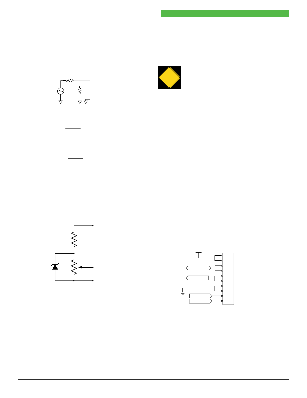
REMOTE LIMIT STATUS LED CIRCUIT
current limit resistor between pin J3:3 and ground. Connect
the external LED as shown in Figure 13.
LD STATUS
+5V H1:2
H3:3
Figure 13. Remote LIM I Status LED
SET THE CURRENT LIMIT MORE ACCURATELY
The current limit circuit is designed with a small hysteresis,
which causes the limit circuit to trip at a slightly lower current
+5V is the supply voltage:
+5V – V
calculated on page 13.
CHANGE THE PHOTODIODE RANGE,
TYPE A & B LASERS
The photodiode current range and transfer function can be
adjusted by adding an external resistor. This feature is useful
when the photodiode current of your laser falls in a range
that does not allow maximum measurement sensitivity on
the PLDxK-CH driver.
Figure 14 shows the internal resistor network of the
H1:2
J2:1
PD Range
Switch
554 Ω
5 kΩ
PD Range = L
µA
µA / V
PD Range = H
2.5 V * 106
R || 500 Ω
Range = µA
µA /
V
6
R || 500 Ω
10
Transfer
Function =
2.5 V * 106
R || 5 kΩ
Range =
6
R || 5 kΩ
10
Transfer
Function =
R || 5 kΩ
R + 5000
R * 5000
=R || 500 Ω
R + 500
R * 500
=
PD Anode
COMMON
R
Internal Electronics External Electronics
ΩΩ
Figure 14. Adjusting the PD Range,
Type A & B Lasers
CHANGE THE PHOTODIODE RANGE,
TYPE C LASERS
The photodiode range and transfer function can be adjusted
ADDITIONAL TECHNICAL
INFORMATION
This section includes useful technical information on these
topics:
• Remote Limit Status LED Circuit
• Set the Current Limit More Accurately
• Change the Photodiode Range, Type A & B Lasers
• Change the Photodiode Range, Type C Lasers
• Change the Analog Input Modulation Transfer
Function
• External Setpoint Circuit
• Important Information on Grounding
• Fine Tune Deep Modulation
• PLD5K-CH and PLD10K-CH Revision A
• Cable Lengths and High Current
• Add Laser Diode Protection for Long Cables
• Additional Noise Filtering
• Monitor Calibration Circuit
• Revision B Timing Characteristics
• Product Variations
• Negative Laser Power Supply Wiring
• Output On/O and Current Limit Timing
• Parallel PLDs for Higher Current
• Power Supplies and Noise
• Safe Operating Area Calculation
© 2020 www.teamWavelength.com 16
PLDXK-CH SERIES LASER DIODE DRIVER
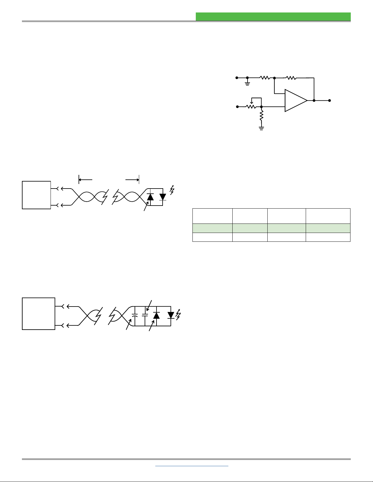
CHANGE THE ANALOG INPUT MODULATION
TRANSFER FUNCTION
The analog input modulation transfer function can be
changed by adding a voltage divider resistor network
external to the PLDxK-CH driver. Figure 15 illustrates a
simple circuit.
R2
ANALOG
INPUT
V
COMMON
Keep R1 and R2 below 100 kΩ
for maximum accuracy.
IN
R1
R2 + R1
R2
New
Transfer
Function
Old Transfer Function
=*
Example:
(for PLD10K-CH)
R1 = 9 kΩ
R2 = 1 kΩ
1 + 9
1
New
Transfer
Function
2.3 A / V = 230 mA /
V
=*
Figure 15. Changing the Analog Input
Modulation Transfer Function
EXTERNAL SETPOINT CIRCUIT
An external trimpot circuit can be used to adjust the laser
Figure 16.
R1
R2
D1
Analog Input
Pin J3:5
V
+5V
Common
Pin J3:1
= Supply voltage (5 to 30 V)
D1 = Bandgap reference* (LM4040)
R1 = 2.2 kΩ, 1 W resistor
R2 = Trimpot, 10 kΩ to 100 kΩ
* must be at least 1 volt greater than
the voltage value of D1.
V
+5V
V
+5V
Figure 16. Trimpot Circuit for Analog Input
IMPORTANT INFORMATION ON GROUNDING
Some laser diodes connect the laser anode or cathode to
grounding to ensure safe operation of the PLDxK-CH and
laser.
!
that the anode will be connected to earth ground when
the laser is installed in a benchtop mount or in your laser
the case, it is critical that the negative terminal of the power
supply remain isolated from earth ground.
FINE TUNE DEEP MODULATION
16 V electrolytic capacitor between the power terminals
directly connected at the PLDxK-CH.
PLD5K-CH AND PLD10K-CH REVISION A
Revision A of the PLD5K-CH and PLD10K-CH use a
Figure 17
LD Cathode
LD Anode
PD Cathode
PD Anode
J1 +5V
LD Cathode
LD
Anode/LD Supply
Ground
PD Cathode
PD Anode
+5V
Figure 17. Revision A Connector
PLD5K-CH and PLD10K-CH
© 2020 www.teamWavelength.com 17
PLDXK-CH SERIES LASER DIODE DRIVER
CABLE LENGTHS AND HIGH CURRENT
The length and gauge of cable from the power supply or
to the laser diode can impact performance. The resistance
and inductance of the wire can reduce bandwidth or cause
the voltage to the PLDxK-CH to droop.
approaches the limit setting, then the power supply cables
470 µF capacitor across pins H1:1 and H1:2 to minimize
droop. Always twist the wire pairs to eliminate reactance.
ADD LASER DIODE PROTECTION FOR LONG
CABLES
With a cable longer than two feet, add a Schottky diode
across the laser diode, see Figure 18.
Laser
Diode
Schottky
Diode
(1N5818)
Cable > 2 feet
H1:3
H1:4
LD Anode
LD Cathode
Figure 18. Long Cable Laser Protection
ADDITIONAL NOISE FILTERING
The PLDxK-CH drivers provide low-noise current to the
needed. Refer to Figure 19
LD Anode
LD Cathode
Schottky
Diode
(1N5818)
0.1 µF
10 µF
H1:3
H1:4
Figure 19. PLDxK-CH Output Filter
MONITOR CALIBRATION CIRCUIT
Figure 20
Common
Pin J2:1
+
10 kΩ
10 kΩ
10 kΩ
20 kΩ
-
Monitors
Pin J2:2, 3, 4 Calibrated
Current
Setpoint
Figure 20. Monitor Calibration Circuit
REVISION B TIMING CHARACTERISTICS
Table 4 describes the timing and bandwidth characteristics
of the PLDxK-CH Series Revision B units.
Table 4. Output Timing, Revision B
MODEL TURN-ON
TIME
TURN-OFF
TIME
SLOWSTART
DELAY
PLD5K-CH 6.8 µsec 6.8 µsec
PLD10K-CH 10 µsec 12 µsec
PRODUCT VARIATIONS
We design and manufacture our products in-house, and
high-volume manufacturing.
Examples of past Product Variations include:
•
•
laser controller system
• Changing the controller input voltage

© 2020 www.teamWavelength.com 18
PLDXK-CH SERIES LASER DIODE DRIVER
NEGATIVE LASER POWER SUPPLY WIRING
Connecting the laser anode to ground will give the best
to drive the electronics and the laser with separate power
grounded.
Connecting the laser driver power supply in this way is
power supply. See Figure 21 for a basic wiring diagram.
A
B
12 V
Figure 21. Basic Negative Supply Operation
anode is grounded, the voltage at the cathode is -12 V with
power supply.
The laser anode can be connected to earth ground, but only
if no other components in the system are earth-grounded.
POWER THE PLDxK-CH
The PLD5K-CH and PLD10K-CH can use a single power
supply for the laser and the electronics if the forward voltage
of the laser diode is not too great. Figure 8 on page 10
illustrates single-supply operation with the laser driven by a
negative voltage power supply.
use a separate negative voltage laser power supply if the
forward voltage of the laser is greater than the compliance
cases, the laser can be driven by a negative voltage power
supply for the best possible noise performance.
The electronics of the PLDxK-CH driver must be biased
when a negative voltage power supply is used to drive the
laser.
to provide a 5 V bias across the electronics. Since the
electronics and laser current source are internally grounded,
the voltage at Point C must be 5 V positive with respect to
Point A.
Figure 22 (this is the same
Figure 8
advantages:
• Simplicity: a external 5 V power supply is easy to
procure, or can easily be designed into a laser control
system.
• Noise performance: the power supply and the electronics
share the ground reference point, so even if the voltage
across the control electronics remains constant. This
may be important if the laser drive current is modulated.
Driver
Electronics
A
B
C
V
S
VS= 5 VDC
Internal Ground
Connection
12 V
Figure 22. Negative Supply Operation,
5 V Electronics Power Supply
Another solution is to bias the electronics with a power
supply in series with the control electronics, shown in
Figure 23. This solution is less favorable because noise
the voltage across the control electronics.
A
B
C
VS
12 V
V
S
= 7 VDC
Internal Ground
Connection
Driver
Electronics
Figure 23. Negative Supply Operation,
7 V Electronics Power Supply
© 2020 www.teamWavelength.com 19
PLDXK-CH SERIES LASER DIODE DRIVER
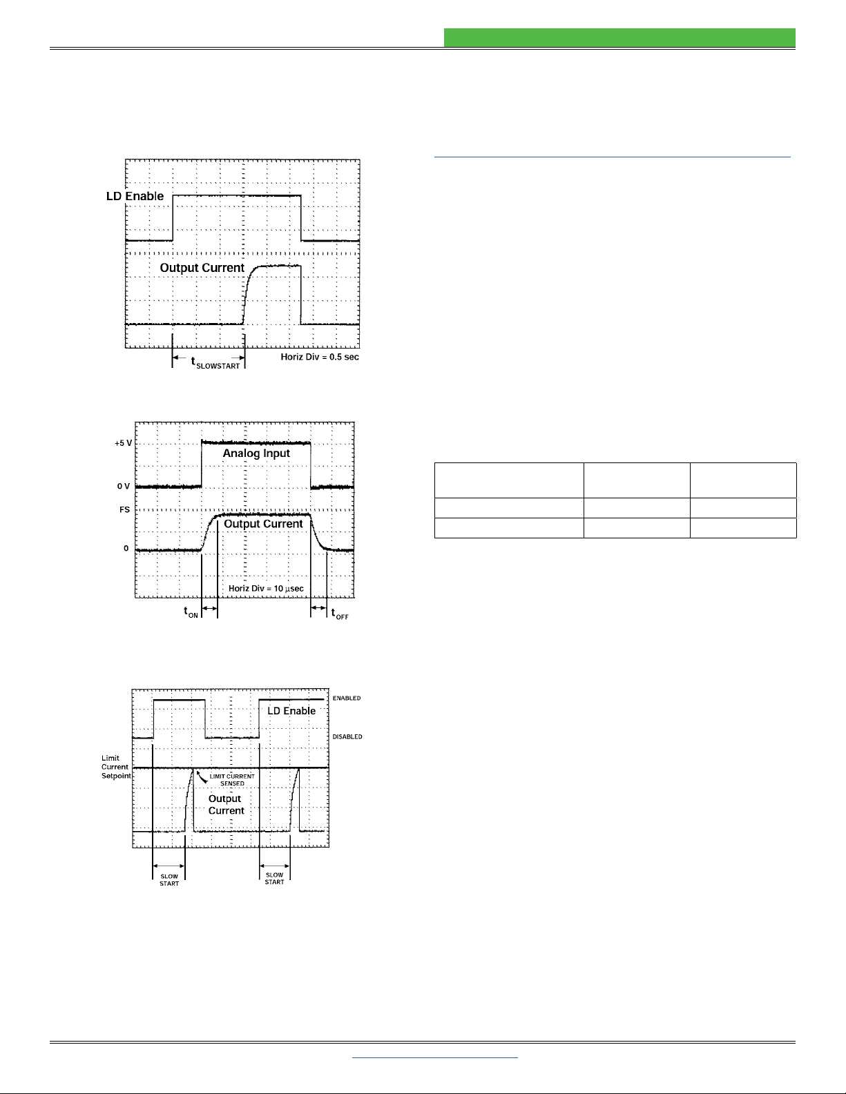
OUTPUT ON/OFF AND CURRENT LIMIT TIMING
Figure 24 through Figure 26 illustrate the output turn-on
delay, output rise and fall times, and current limit response.
Figure 24. Output Turn-On Delay
Figure 25. Output Rise / Fall-Time
Figure 26. Current Limit Response
PARALLEL PLDS FOR HIGHER CURRENT
Multiple PLDxK-CH drivers can be connected in parallel to
drive higher current. Contact the factory for more information
on how to do this safely, or see Application Note AN-LD06:
www.teamwavelength.com/download/applicationtechnotes/an-ld06.pdf
POWER SUPPLIES AND NOISE
The PLDxK-CH drivers deliver stable current with low noise,
performance of the driver.
We recommend using a regulated linear supply for the
best noise performance, but depending on your application
supply. Each case must be evaluated because a switching
work in your application.
MODEL MAX
VOLTAGE
MAX
CURRENT
PWRPAK-13A-5V 5 V 13 A
PWRPAK-11A-12V 12 V 11 A
© 2020 www.teamWavelength.com 20
PLDXK-CH SERIES LASER DIODE DRIVER
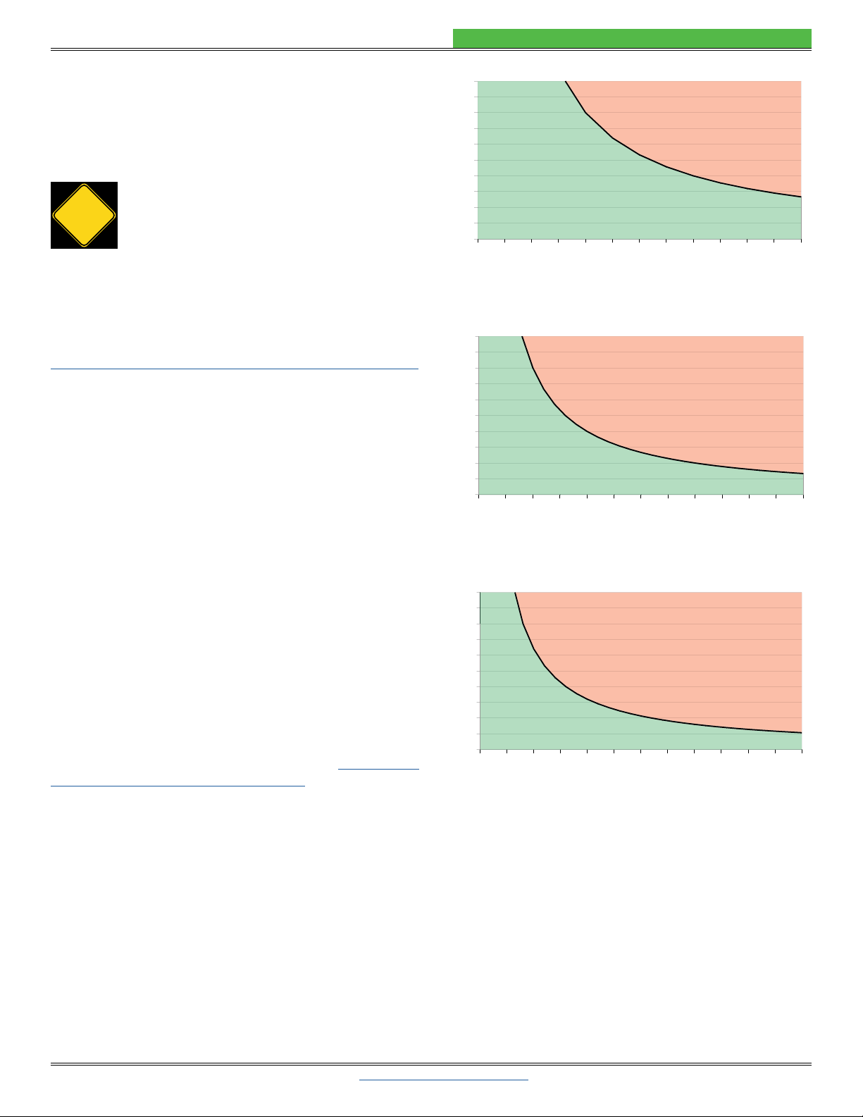
SAFE OPERATING AREA CALCULATION
determined by the amount of power that can be dissipated
exceeded, permanent damage can result.
!
Refer to the Wavelength Electronics website for the most
is fast and easy to use, and also takes into consideration
operating temperature.
www.teamwavelength.com/support/design-tools/soa-ld-calculator/
however we recommend you use the online tools instead.
Follow these steps to determine if the driver will be operating
•
voltage (VMAXMAX
• Calculate the voltage drop across the controller:
VS- VMAX (VS
• Mark V on the X-axis, and extend a line upward
• MAX
until it intersects the V line
• S
• Extend a diagonal line from VSto the intersection of the
VMAX
•
changed so that less power is dissipated within the driver.
See Wavelength Electronics Application Note AN-LDTC01:
The Principle of the Safe Operating Area for information on
shifting the Load Line.
After changing any of the operating parameters, recalculate
contact Wavelength Electronics for assistance.
Voltage Drop (V)
Current (A)
0.02.5 5.07.5 10.0 12.5 15.0 17.5 20.022.525.027.530.0
0.0
0.5
1.0
1.5
2.0
2.5
3.0
3.5
4.0
4.5
5.0
Figure 27. SOA for PLD5K-CH
Voltage Drop (V)
Current (A)
0.02.55.07.510.0 12.5 15.017.5 20.0 22.5 25.027.5 30
.0
0.0
1.0
2.0
3.0
4.0
5.0
6.0
7.0
8.0
9.0
10.0
Figure 28. SOA for PLD10K-CH
Voltage Drop (V)
Current (A)
0.02.55.07.510.0 12.5 15.017.5 20.0 22.5 25.027.5 30.0
0.00
1.25
2.50
3.75
5.00
6.25
7.50
8.75
10.00
11.25
12.50
Figure 29. SOA for PLD12.5K-CH
This manual suits for next models
3
Table of contents
Other Wavelength Electronics DC Drive manuals


