Yaesu FRG-100 Manual

-
-
-
FRG-100
Technical Supplement
YAESU MUSEN CO., LTD.
C.P.0,
Box
1500,
Tokyo, Japan
YAESU U.S.A.
17210
Edwards Rd., Cerritos, California 90701, U.S.A.
YAESU EUROPE B.
Vi
Snipweg
3.1118AA
Schipol,
The Netherlands

Contents
Introduction
.
.
.
.
.
.
.
.
.
.
.
.
.
.
.
.
.
.
.
.
.
.
.
.
.
.
.
.
.
.
.
.
.
.
.
.
.
.
.
.
.
.
.
.
.
.
.
.
.
.
.
.
.
.
.
.
.
.
.
.
.
1-l
Chip
C’mponent
Information . . .
-.
. . . . . .
l
.
-
-.
.
-
-.
. . .
*.
. . . . . . . . . . . . . . . . . . . . .
l-3
Cse
Disasembly &
&cuit
&ard
Access
-
-
l
.
-
-
-
l
-
l l l
-
..
-
-
-
-
-
l l l
-
-
.
-
-
.
l
-
-
-
‘J-1
Main Unit
2-l
Local Unit 2-l
Display Unit
2-3
Pilot Lamp
&
Lithium Battery
Replacement
2-3
Resetting the Microprocessor 2-3
&cuit
Des&ption
.........................
.
...
. . .
.......m....
...
.....
. . . .
3-l
Alignment
. . . . . . . . . . . . . . . . . . . . . . . . . . . . . . . . . . . . . . . . . . . . . . . . . . . . . . . . . . . . . . . .
4-l
Aligument
Preparations
&
Precautions 4-l
Local
Uuit
4-2
Reference Oscillator
4-2
2nd Local Oscillator
4-2
vco 4-2
vco
1&2
4-2
vco 3
4-2
vco 4
4-2
vco 5
4-2
Main Unit
4-2
2nd
Local Amplifier
4-2
IF
Interstage Transformer
4-2
IFGain 4-2
S-Meter
Full
Scale
4-3
Noise
Blanker
4-3
SSB
Squelch
Threshold 4-3
Beep Leve
4-3
Block
&
Interconnection
J)iagrams
.
.
.
.
.
.
.
.
.
.
.
.
.
.
.
.
.
.
.
.
.
.
.
.
.
.
.
.
.
.
.
.
.
.
.
.
.
.
.
.
.
5-l
PCB
Diagram
&
Pa&
List
.
.
.
.
...
.
.
.
.
.
.
.
.
.
.
.
.
.
sm..
.
.
l
m.
.
.
l l l
a
l
.
.
.
.
.
.
.
.
.
.
.
6-1
Main Unit
6A-1
Local
&
OSC Unit
6B-1
PLL DDS Unit 6C-1
CAR DDS Unit
6D-1
Display Uni t
6E-1
SQL,VR,ENC
&
HP Unit 6F-1
FM
hit-lOO(
Option) 6G-1
TCXO-4(
Option) 6H-1
Mechanical
Details
.
.
.
l
.
-
-
+
-.
l
.
.
.
.
.
.
.
.
.
.
.
.
l
.
.
.
.
.
.
.
.
.
.
.
.
.
.
.
.
.
.
.
.
.
.
.
.
.
.
.
.
.
.
.
.
7-l

Introduction
This manual provides technical inf
orma-
tion necessary for servicing the FRG-100 gen-
ral coverage communications receiver. It does
not include information on specifications, in-
stallation, and Operation, which are described
in the FRG-100 Operating Manual, provided
with each receiver, or on FRG-100 accessories,
which are described in manuals provided
with
each.
Servicing ‘this equipment requires exper-
tise in handling surface-mount components.
Attempts by non-qualified persons to Service
this equipment may result in permanent
dam-
age not covered by the warranty.
While we believe the technical information
in this manual to be correct, Yaesu assumes no
liability for darnage that may occur as a result
of typographical or other errors that may be
present. Your cooperation in pointing out any
inconsistencies in the technical information
would be appreciated.
Yaesu Musen reserves the right to make
changes
in this receiver and the alignment
procedures, in the interest of technological
improvement, without
notification
of the
0 wners.
l-l
FRGl
00
Techm*cal
Supplement

Chip Component Information
The diagrams below indicate some of the
distinguishing features of common
Chip
com-
ponents.
Ceramic Capacifors
-i_
f
Tantalum
Capacifors
Negati
(Unit
1
mm)
Type L W T
Resistors
INDICATED LETTERS
1 2 3 4
557s
90
0
Type
RMC
l/lOW, 1/16W
Marking*
100,222,473*---
10’s unit
1’s
unit
Multiplier
00
10"
1
1
10’
I
22
lo’
1
33
10”
4410’
55
1
OS
66
10”
Examples
1
100 =
ion
222 =
2.2kn
473 =
47k0
1-3
FRGl
00
Technicd
Supplement

Chip Component Information
Replacing
Chip Components
Chip components are installed at the
fac-
tory
by a series of robots. The first one
places
a small spot of adhesive
resin
at the location
where each part is to be installed, and later
robots handle and place
Parts
using vacuum
suction.
For
Single
sided boards, solder Paste is
ap-
plied and the board is then baked to harden
the resin and flow the solder. For double sided
boards, no solder Paste is applied, but the
board is baked (or exposed to ultra-violet
light) to
eure
the resin before dip soldering.
In our laboratories and Service shops, small
quantities of chip components are mounted
manually by applying a spot of resin, placing
with tweezers, and then soldering by very
small dual streams of hot air (without physi-
cal contact during soldering). We remove
Parts by first removing
solder
using a vacuum
suction iron, which applies a light steady
vac-
uum at the iron tip, and then breaking the
adhesive with tweezers.
The special vacuum/desoldering equip-
ment is recommended if you expect to do a lot
of
Chip
replacements. Otherwise, it is usually
possible to remove and replace
Chip
compo-
nents with only a tapered, temperature-con-
trolled soldering iron, a set of tweezers and
braided
topper
solder
wick.
Soldering iron
temperature should be below 280” C
(536”
F).
Precautions
for
Chip
Replacement
DO not disconnect a
Chip
forcefully,
or the
foil Pattern may peel off the board.
Never re-use a
Chip
component. Dispose of
all removed
chip
components immediately to
avoid mixing with new
Parts.
Limit soldering time to 3 seconds or less to
avoid damaging the component and board.
Removing Chip Components
Cl
Remove the
solder
at
each
joint, one joint at a
time, using
solder
wick
whetted with
non-
acidic fluxes as shown below. Avoid applying
pressure, and do not attempt to remove
tin-
ning
from
the
chip’s
electrode.
0
Grasp the
chip
on both sides with tweezers,
and gently twist the tweezers back and forth
(to break the adhesive bond) while
alter-
nately heating
each
electrode.
Be careful to
avoid peeling the foil
traces
from the board.
Dispose of the
chip
when removed.
0
After removing the
Chip,
use the topper braid
and soldering iron to
wick
away any excess
solder
and smooth the land for installation of
the replacement part.
FREI
00
Techmkd
Supplement

Chip Component Information
--
Installing a
Replacement
Chip
As the value of some
Chip
components is
not indicated on the body of the
Chip,
be
care-
51l
to get the right part for replacement.
0
Apply a small amount of
solder
to the land on
one side where the
chip
is to be installed.
Avoid too
much
solder,
which
may
Cause
bridging (shorting to other
Parts).
.I.
0
Hold the
chip
with tweezers in the desired
Position, and apply the soldering iron with a
motion line as indicated by the arrow in the
diagram below. DO not apply heat for more
than 3 seconds.
0
Remove the tweezers and
solder
the
elec-
trode on the other side in the
manner
just
described.
l-5
FRGl
00
Techmkd
Supplement
Case Disassembly & Circuit Board Access
-
Main
Unit Local
Unit
0
Turn off the
receiver
and disconnect all
ca-
bles.
0
Place the set on a stable work surface, and
remove the 8 screws affixing the top cover
(Figure
1).
Figure 1.
0
Carefully remove the top cover, paying spe-
cial
attention to the wire connecting the loud
speaker to the main unit. The plug
tan
be
removed from the socket on the main board
if desired (remember to reconnect before at-
tathing
the top cover again).This exposes the
component side of the Main Unit.
0
To remove the main unit, remove the 8 screws
affixing the unit and the screws affixing the
antenna terminal and EXT DC connector on
the rear
Panel
(Figure 2).
Figure 2.
0
To access the local unit, remove the 8 screws
affixing the bottom cover (Figure 3).
Figure 3.
To remove the local unit, remove the 7 screws
affixing the unit, and the 2 screws used on the
CAT connector on the rear Panel. This
ex-
poses the component side of the Local Unit
(Figure 4).
Figure 4.
2-l
FRGl
00
Tmlmical Supplement

Case Disassembly
&
Circuit Board Access
Display
Unit
0
To access the Display Unit (including
poten-
tiometer, squelch, rotary encoder and
head-
phone jack), remove both the top and bottom
covers
as previously described, then remove
the 2
middle
screws from both edges on each
side of the display unit (Figure 1).
Figure 1.
0
Next
Zoosen
the 2 remaining screws Gently
pull the unit away from the Chassis and fold
it down (Figure 2).
Figure 2.
Cl
To remove the Display Unit, slightly
loosen
the hex nut affixing the main dial (do
not
uyIscrez.u
it!) and pull it
Off,
then remove the 2
screws located underneath (Figure
3).
Cl
Gently pull off the VOL, SQL and MEM
knobs, then remove the 4 screws (2-each, top
&
bottom) attaching the front
Panel
to the
display unit Chassis.
Figure
3.
0
0
0
0
0 Remove the wiring connectors from the SQL
and VOL controls on the rear of the Display
Unit.
0
Gently press in the plastic catch
which
mates
with the tab on the Display Unit circuit board
to release and lower the front
Panel
(Figure
4).
Figure 4.
Next, using a small flat screwdriver, gently
pry out and remove the wiring connector
from the back of the MEM knob, then remove
the front Panel.
Gently
pull
the POWER,
AlT
(2pcs.),
NB,
and AGC buttons out from the Panel. Then
remove the spring
screw,
nylon
washer,
threaded
brass collar and
washer
affixing the
rotary encoder shaft to the Chassis.
Remove and the 6 screws aff ixing the Display
Unit circuit board to the Chassis (Figure 5).
Last, carefully remove the three wiring con-
nectors from the bottom edge of the Display
Unit circuit board to free the unit.
Figure 5.
FRGlOO
Tedmicd
Supplement
~__~_I_s_
_.-_.l..-
.
-_.______._._-
..“.-----
.._.”
--.--..
--.
-

Case Disassembly
&
Circuit Board Access
Pilot
Lamp
Replacement
Cl
Disconnect all cables and remove the top and
bottom covers as previously described.
0
Remove the 2 middle screws from both edges
of the display unit and
loosen
the 2 lower
screws at the edge of each side.
‘Loosen
0
Locate the Pilot light then pull it out from it’s
grommet,
trace
the two blue
wires
leading
from the bulb to TP1005
&
TP1006 on the
corner
of the circuit board as shown below.
Carefully
unsolder
these
wires
to remove the
lamp and resolder the replacement lamp
as-
sembly (polarity of the
wires
is not
impor-
tant).
To Change the backup cell, use your fingers
to remove the old cell from it’s holder (do not
grab it with metal
tweezers
or pliers, as that
could short it out). Replace only with Sony
lithium type CR2032 (Yaesu Part No.
Q900564),
or
equivalent .
Removing Lithium
Ce11
Slide
cell
inward, then pry up to eject
Inserting Replacement Battery
Pilot Lamp TP1005
&
TP1006
Battery replacement
The lithium backup battery tan be re-
placed by removing the bottom cover (as pre-
viously described). Battery location is shown
below.
Slide battery downward through slot, then
inward and release
Resetting the microprocessor
Functional Problems involving
frequency,
mode and memory selection
tan
sometime be
resolved by simply resetting the microproces-
sor. There are two ways to reset the CPU in the
FRG-100, both of which clear the contents of
all memories, leaving them at the factory de-
faults.
Soft Reset
The procedure relies on a ROM routine
which should normally suffice to correct most
operating malfunctions.
0
Turn the
receiver
Off,
then hold the MEM
CLEAR button while switching the
receiver
back on. If the Problem still persists, proceed
to the hard reset.
FRGlOO Techmixl Supplement
2-3

Case Disassembly
&
Circuit Board Access
Hard Reset
D
Turn the receiver off, then disconnect the DC
power Source. Turn the BACK UP
switch
on
the rear
Panel
to OFF. Reconnect the DC
power Source, then turn the receiver back on.
BACK UP
ON OFF
BACK
Ul?
SWITCH
2-4
FRGl
00
Technical Supplement

Circuit Description
This description, together with the block
diagram, is intended to provide a general
un-
derstanding of the electrical functions of the
circuits of the FRG-100. Such an
under-
standing is necessary for troubleshooting the
receiver. Refer to the schematics diagrams and
Parts
lists
for specific component and wiring
details.
Front-End Stages
Incoming RF from the antenna jack is deliv-
ered to the main unit after passing through a
9:l
impedance transformer Tl004 (if
Hl-Z
an-
tenna is selected using the rear-Panel switch)
and surge suppresser D1005, which removes
high voltage electrostatic pulses which might
otherwise darnage components in the front-
end. It is then low-pass filtered and attenu-
ated (if enabled). The received
Signal
is then
impedance transformed by transformer
T1018, then band-pass filtered to suppress
in-
termodulation by Signals from other bands.
The correct bandpass filter is selected by BCD
control Signals from the PLL unit, and
de-
coded by Q1032
(SN74LS145N).
The
Signal
is
then once again impedance transformed by
T1005, before entering the 1st mixer
Stage.
._.
The
Signal
then enters the balanced 1st
mixer, consisting of
Q1009/Q1013
(2SK125X2),
along with the 1st local oscillator
output from the
local
unit (47.260
w
77.210
MHz) which has been amplified by Q1006
(2SC2053), and low-pass filtered by C1014,
L1005, C1013, L1004, and
C1012.
The result-
ing 47.21 MHz 1st mixer
product
Passes
through monolithic crystal filters
XFlOOl
and
XF1002 (
f
20 kHz BW) where other unwanted
mixer products are stripped away to produce
the filtered 1st IF Signal.
IF
Stages
The filtered 1st IF
Signal
is then amplified
,^.
by
Q1011(3SK179),
and applied to balanced
2nd mixer
QlOlO
&
Q1012
(2SK302x2), which
also receives the 2nd local
Signal
generated
from 46.775 MHz crystal
X2002
and amplified
by
QlOO8
(2SC2620),
to produce the 455 kHz
2nd IE When FM Operation is selected, a por-
tion of this 455 kHz product of the 2nd mixer
is buff er-amplified by
QlO38
and delivered to
the optional FM
UNIT-1
00
for detection(when
installed) For other modes, the 455 kHz
Signal
is Passes through the noise blanker gate
(D1009,
DlOlO
&
D1014) and is then filtered
by ceramic filters CF1 001, CF1002, or CF1 003
(depending on selected mode) where other
products are stripped away
Final IF
amplification
is provided by
Ql018, QlO17, and
Q1016
(3SK131-V12)
be-
fore the
Signal
is applied to buffer amplifier
Q1016
(3SK131-V12) and then enters detec-
tion
circuitry.
For SSB and CW modes, the amplified IF
Signal
is applied to the product detector
con-
sisting of D1033, D1038,
DlO39,
and D1040
(lSS198x4). Here, it
is
mixed with the appro-
priate BFO(carrier)
Signal
for either LSB, CW
or USB from the DDS unit, having been buff-
ered by Q1028. The detected Signal then
Passes
through a LPF consisting of
R1129
and
Cl141 before delivery to analog switch
Q1023-
4. The
Signal
enters the active filter
Ql026-1,
which functions as a low pass filter for audio
before delivery to analog switch
Ql501.
For AM reception, another buffered output
from the 2nd IF is detected by D1032, the
output of which serves as both the detected
AM
Signal
and AGC. This
Signal
then
Passes
through the LPF formed by
R1208
and Cl130
before delivery to analog switch Q1023-3 and
on for audio amplification.
Aud io Amp
lif
iers
The low level detected audio in all modes
pass through mute switch Q1023-l(when not
muted by the
squelch
control lines), and then
buffer amplifier
Q1026-2.
The
Signal
Passes
through another mute circuit
Q1031
&
(21046
(DTC144EK)
and is mixed with beeper audio
from the microprocessor having passed
through the LPF and VR1005. The mixed
audio is amplified by Q1034 (TDA2003H) to
drive a 4
w
8
Q
loudspeaker or headphone.
The output from Q1034 is controlled by VOL
1
.
FRGI
00
Techm*cal
Supplement

Circuit Description
Potentiometer VR3601 located on the VR
Unit. A
Sample
of the pre-amplified audio
@
600
&2
is also delivered to the REC jack on the
rear
Panel.
Noise
Blanker
&
AGC Circuit
In the AM, SSB and CW modes, when the
noise blanker is on, a Portion of the 455 kHz
2nd IF
Signal
is tapped from the output of
T1011,
then
Passes
through noise blanker
am-
plifiers
41004
&
QlOO5
(3SK131-V12), and
de-
tected by D1003
&
D1004, then fed back to the
amplifiers Q1004
&’
QlOO5,
controlling their
gain.
The response time of this loop is
de-
signed so that noise pulses detected at D1003
&D1004
produce a strong DC pulse for the
duration of each RF noise pulse. This DC
blanking
Signal
is returned to the noise blank-
ing gate Controller
(D1009,
DlOlO
&
D1014),
switching them off during the noise pulse and
preventing the 2nd IF
Signal
from reaching
the narrow IF filters while the noise is present.
Receiver AGC is provided for all modes,
with a selectable fast or slow decay. The out-
put
Signal
from buffer amplifier
QlOl9
is rec-
tified by AGC detector D1026 and D1027
(lSS198x2), and then delivered to AGC
am-
plifier Q1020
(2SC2712).
The
Signal
is
proc-
essed by
QlOl5
(2SJ125),
then amplified again
by
Q1014-1
and delivered to
QlOll,
QlOl8,
and
Q1017
to control amplifier gain, S-meter
and squelch level.
PLL Frequency Synthesizer
The PLL section on the Local Unit consists
of Main Loop, DDS and the 2nd local oscilla-
tor circuitry. The PLL IC
Q2030
(CX-7925B)
contains a reference oscillator/divider, serial-
parallel data latch, programmable divider,
and a
Phase
comparator.
1st
Local
Signal Generation
The 1st local
Signal
(47.260
-
77.210 MHz)
is generated by PLL Synthesis
under
control of
CPU on the Local Unit. In the main loop, one
of VCOs
Q2015-Q2018
is activated by the
CPU and selected via Q2040
(M54564P)
ac-
cording to the frequency of Operation. The
output of the selected VCO is buffered by
Q2045
(2SK192)
and
Q2011
(2SC535)
before
delivery to mixer Q2012
(uIIX1037H)This
sig-
na1
is then mixed with the DDS
Signal
and
low-pass filtered, buffered by Q2021(2SK192)
and amplified by Q2024
(2SC535)
before be-
ing returned to PLL IC Q2030.
In the main divider/phase comparator sec-
tion of PLI, IC, the VCO
Signal
is divided by
128, according to a control
Signal
(serial
di-
vider programming data) from the CPU to
produce 83.
.92
kHz.
This
Signal
is then applied to the Phase
detector section for Phase-comparison with
the 10.4875 MHz reference
Signal
from the
OSC
UN IT. Any
Phase
differente
between the
two
Signal
will produce a 5-V pulsed-DC out-
put with pulse duration depending on the
Phase differente. This pulse train is converted
to DC by
charge
pump
42025
(2SK184)
and
Q2023
(2%3732),and
low-pass filtered to
pro-
duce the varactor control voltage (VCV), and
then is applied to the varactor D2002
-
D2005
(lSV103x4)
in the selected VCO to
Cause
the
VCO oscillating frequency to be Phase-locked
to the 10.4875 MHz reference.
The
PLL,
local
Signal
for Loop 1 is the prod-
uct of either Loop 1 Local Mixer
(Q2012),
or
the product of the output of this mixer further
mixed with the 10.4875 crystal reference
sig-
nal, according to the band of Operation.
2nd
Local
Signal Generation
A Portion of 2nd local oscillator
Signal
(46.755 MHz),
which
is derived from
Q2031(2SK:192)/X2002,
is delivered to mixer
Q2028
(SN-16913),
it also is applied to the 2nd
local amplifier (on the main unit) after
attenu-
ation and passing through the LPF formed by
L2023, C21.46 & C2147.
The sampled reference Signal (10.48576
MHz), which is generated by Q2030, is halved
by frequency divider
42032-2.
The output
from the divider (5.24288 MHz) is low-pass
filtered, then mixed with the DDS output
(286.16
-
368.07 kHz) in mixer Q2034
(SN1
6913),
which is also
controlIed
by the
MPU. The output from Q2034 is band-pass
filtered (5.57 MHz) by CF2001 before delivery
to mixer Q2028
(SN16913)
along with the 2nd
local Signal. The mixer product is band-pass
FRGl
00
Techmkd
Supplement
Circuit Description
filtered before
amplification
by Q2019
(2SC535),
and then applied to the mixer of the
main loop Q2012
(uPC1037H)
as a sub-loop
Signal.
Although the reference frequency of the
main loop is 81.92 kHz, a 10 Hz receiving
frequency step is obtained by mixing a
sub-
loop
Signal
with the main loop. The VCO is
thus Phase-locked to the reference Signal.
Miscellaneous Con
trol
Logic
Band selection for the PLL Loop 1 Local
Signal
is provided from the CPU by encoder
Q2005 (M14558CP) and
switch
driver
42040
(M54564P).
Whenever either VCO Loop be-
Comes
unlocked, and unleck line (from pin 8
of Q2030)
controlled
by Q2027
(BAlA4P)
sig-
nals the CPU, which then mutes
receiver
audio and blinks the display until the
PLLs
resume leck.
The MPU provides band
(BPF)
selection on
the Main Unit via
latch
Q1032(SN74LS145N),
and
mode/filter
selection using switching
gates Q1023-2-Q1023-4 and
Q1054.
Rotary encoded tuning data from the main
dial is
processes
by dial
counter
Q2044
(FQ7924), and transferred to the MPU via an
S-bit data bus.
Q2041
contains a real-time
clock with reference oscillator crystal.
“V
FRGI
00 Techmkal Supplement

The FRG-100 is carefully designed to allow
the knowledgeable Operator to make nearly
all adjustments for various Station conditions,
modes and Operator preferences simply from
the controls on the front and rear Panels, with-
out having to open the
case
of the transceiver.
The FRG-100 Operation manual describes
these adjustments, plus certain internal
set-
tings.
..-
The following procedures cover the
some-
times critical and tedious adjustments that are
not normally required once the transceiver
has left the factory. However, if darnage
oc-
curs
and some Parts subsequently are
re-
placed, realignment may be required. If a
sudden Problem occurs during normal opera-
tion, it is likely due to component failure;
re-
alignment should not be done until after the
fault component has been replaced.
We recommend that
servicing
be
per-
formed by authorized Yaesu Service techni-
cians,
experienced with the circuitry and fully
equipped for repair and alignment. So, if a
fault is suspected, you should contact the
sell-
ing dealer for instructions regarding repair.
Authorized Yaesu Service technicians have
the latest modification information, and
re-
align all circuits and make complete perform-
ante
Checks
to ensure compliance with
factory specifications after replacing faulty
components.
Those who do undertake any of the follow-
ing alignments are cautioned to proceed at
their own risk. Problems
caused
by
unauthor-
ized attempts at realignment are not covered
by the warranty
policy.
Also, Yaesu must
re-
serve the right to change circuits and align-
ment procedures in the interests of improved
Performance, without notifying owners.
,..
Under no circumstances should any align-
ment be attempted unless the normal function
and Operation of the receiver are clearly
un-
derstood, the
Cause
of the malfunction has
been clearly pinpointed and any faulty
com-
ponents replaced, and the need for realign-
ment determined to be absolutely
necessary.
The following test equipment (and
thor-
ough familiarity with it’s correct use) is neces-
sary for complete realignment. Correction of
the Problems caused by misalignment result-
ing from use of improper test equipment is
not covered under the warranty
policy.
While
most
Steps
do not require all of the equipment
listed, the interactions of some adjustments
may require that more complex adjustments
be performed afterwards. DO not attempt to
perform only a
Single
step un less it is clearly
isolated electrically from all other Steps.
Rather, have all test equipment ready before
beginning, and follow all of the
Steps
in a
section in the
Order
they are presented.
0
Digital DC Voltmeter
0
RF Millivoltmeter
Cl
AF Millivoltmeter
0
RF Standard Signal Generator/calibrated
output and
dB
scale,
0
dBp=0.5
PV
0
Frequency Counter
0 FM Unit-100
0 SINAD Meter
Alignment Preparations
G)
Precautions
0
0
0
.
Except where specified otherwise, the
re-
ceiver should be tuned to 14.2 MHz, and the
following controls set as indicated;
all buttons off
all knobs fully CCW (minimum)
After completing one
Step,
read the follow-
mg step to determine whether the same test
equipment will be required. If not, remove the
test equipment before proceeding.
Correct alignment requires that the ambi-
ent temperature be the same as that of the
receiver and test equipment, and that this
temperature be held
constant
between 20 and
30”
C (68
-
88”
F). If the
receiver
is brought into
the shop from hot or
cold
air it should be
allowed some time for thermal equalization
with the environment before alignment.
Alignments must only be made with the
oscillator shields and circuit boards firmly in
.
.
FRGl
00
Techmkd
Supplement
Alignment
place.
Only one extender board (if optional)
should be installed at a time for access
to
the
board being aligned. Also, the
test
equipment
must be thoroughly warmed up before begin-
ning.
Note: Signal levels in
dB
referred
to
in
alignment are based on 0
dBp=0.5pV.
Table note: DC voltages should be within
flO% of those listed in the voltage tables.
Local Unit
(1) Ref erence Oscillator
Cl
0
0
Connect the frequency counter to
TP2005.
Adjust
TC2701 for 10.485760 MHz
f
5 Hz.
If the TCXO is installed,
tonfirm
10.485760
MHz
&5
Hz on the counter.
(2) 2nd Local Oscillator
0
0
0
0
Connect a
50-$2
resistor in parallel with the
frequency counter
across
the
socket
J2011.
Adjust
T2004 for 46.755 MHz
&6OOHz
on the
counter.
Replace the counter with the RF
millivoltme-
ter, and tonfirm at least 45
mVrms.
Connect the RF millivoltmeter to
TMOOl,
and
adjust
T2001, T2002, and T2003 for maximum
indication
(at least 60
mVrms)
on the
meter.
(3) vco
VCOZ
and 2
0 Tune the receiver to 3.999 MHz and select
USB mode.
0 Connect the DC Voltmeter to TP2002
(while
adjusting
VCOs,
connect the DC Voltmeter to
TP2002)
0
Adjust
L2003
for 7.0
&
0.1
V.
0
Confirm the voltage as shown below.
Frequency (MHz)
0.050 Volts DC
0.9
-
1.4
vco3
0 Tune the receiver
to
14.499 MHz in USB
mode.
0
Adjust
L2005
for 7.0 V ti.l
V.
0 Tune the receiver to 8.00 MHz, and tonfirm
1.1 to 1.6 V on the
meter.
vco4
0
0
0
Tune the receiver to 21.999 MHz in USB
mode.
Adjust
L2006
for 7.0 V fl.1 V.
Tune the receiver to 14.500 MHz, and tonfirm
0.8 to 1.3
Volts
on the
meter.
vco5
0 Tune the receiver to 30.000 MHz in USB
mode.
0
Adjust
L:2007
for 7.0 V
rto.1
V.
0
Tune the receiver to 22.000 MHz, and tonfirm
1.4 to 1.9 V on the
meter.
Main
Unit
(1) 2nd Local Amplifier
0
Connect the RF millivoltmeter to TPl003.
0
Adjust
Tl003 on the
local
unit for maximum
(at least
‘500
mV)
on the
meter.
(2) IF Werstage Transformer
0
0
0
0
0
Install
the FM Unit (Option) to the Main Unit,
and select FM mode.
Connect the RF
Signal
generator to the
an-
tenna
jack,
and inject an 80
dBp
Signal
at
14.200 MHz.
Adjust
Tl006 through Tl009 for Optimum
12-
dB
SINAD
(adjust
the
injection
level as
neces-
sary).
Turn the modulation
switch
(of the
Signal
generator)
Off,
and inject an 80
dBp
Signal
at
14.200 MHz.
Adjust
Tl011
through
Tl017
and Tl019 in
succession several times for peak S-meter
in-
dication.
(adjust
the
injection
level as
neces-
sary)
(3) IF Gain
0
Inject 6
dBp
at 14.200 MHz
to
the antenna
jack,
and tune for peak on the
S-meter.
FRGlOO Technical Supplement

Alignment
-_-
0
Adjust
VR1002 for S-l deflection.
(4) S-Meter Full-Scale
0
Inject 100 dBp at 14.200 MHz to the antenna
jack, and tune for peak on the S-meter.
0
Adjust
Tl001 and Tl002 for
minimum
volt-
age on the
meter
(adjust
the injection level as
necessary).
(6) SSB
Squelch
Threshold
0
Adjust
VR1001
for
S9
+60
dB
on the S-meter.
(5) Noise Blanker
0
Cl
With the
receiver
tuned to 14.200 MHz, press
the NB
button.
Inject 40 dBp at 14.200 MHz to the antenna
jack,
and connect the DC Voltmeter to
TP1003.
0 In the USB mode, with no Signal at the an-
tenna jack, set the SQL control to the
ll-
o’clock Position, and
adjust
VR1004
so that
the
squelch
just closes.
(7) Beep Level
0 Set
VR1005
to the
lO-o’clock
position.
_I
T2004 J2011
'SI
T2003
i
z;-a,
,A.Fs
,
T2002
L
l
Y
-T2001
-TP2001
-TP2002
-L2007
-L2006
PL2005
---L2003
-TC2701
-TP2005
I
TP1003
Tl002
Tl001
Tl007
1
Tl0171
VRiOOl VR1002
Tl003
Tl013
Tl014
:
Yr
Tl006
Ort:!
8’
VR1004
--------VRl005
'I
l
Tl019
-Tl015
4-3
FRGl
00
Technical Supplement


Other manuals for FRG-100
2
Table of contents
Other Yaesu Receiver manuals

Yaesu
Yaesu VR-120D User manual

Yaesu
Yaesu FRG-8800 User manual

Yaesu
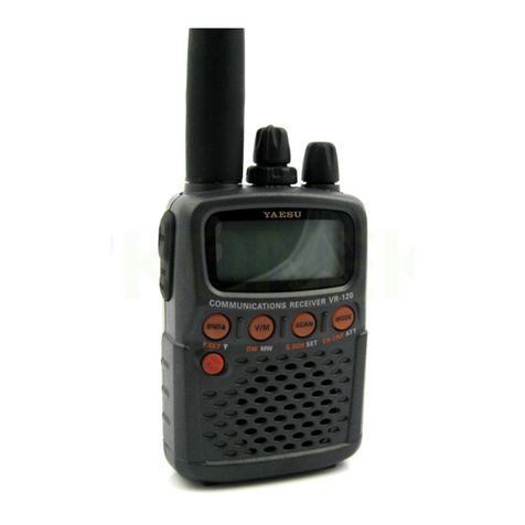
Yaesu FRDX-400 User manual

Yaesu
Yaesu VR-120D Manual

Yaesu
Yaesu FT-710 Technical manual

Yaesu
Yaesu FRG-7700 User manual

Yaesu
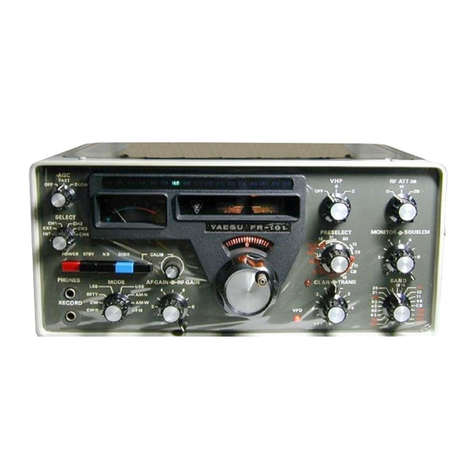
Yaesu FT-901DM User manual

Yaesu
Yaesu FR-101 User manual

Yaesu
Yaesu FT-900 User manual

Yaesu
Yaesu VR-500 User manual