ZMDI ZSPM4521 User manual

Evaluation Kit Description
Rev. 1.00 / February 2013
ZSPM4521
High-Efficiency Photovoltaic Charger for Li-Ion Batteries
Power and Precision

ZSPM4521
Evaluation Kit Manual
Kit Description
February 12, 2013
© 2013 Zentrum Mikroelektronik Dresden AG —Rev. 1.00
All rights reserved. The material contained herein may not be reproduced, adapted, merged, translated, stored, or used without the
prior written consent of the copyright owner. The information furnished in this publication is subject to changes without notice.
2 of 18
Restrictions:
Zentrum Mikroelektronik Dresden AG’s ZSPM4521 Evaluation Kit is designed for evaluation of the
ZSPM4521, laboratory setup, and module development only. This kit must not be used for module production
and production test setups.
Zentrum Mikroelektronik Dresden AG (ZMD AG, ZMDI) shall not be liable for any damages arising out of
defects resulting from (i) delivered hardware (ii) non-observance of instructions contained in this manual, or
(iii) misuse, abuse, use under abnormal conditions or alteration by anyone other than ZMD AG. To the extent
permitted by law, ZMD AG hereby expressly disclaims and User expressly waives any and all warranties,
whether express, implied, or statutory, including, without limitation, implied warranties of merchantability and
of fitness for a particular purpose, statutory warranty of non-infringement and any other warranty that may
arise by reason of usage of trade, custom, or course of dealing.
Contents
1Kit Contents......................................................................................................................................................4
2Introduction.......................................................................................................................................................4
3General Overview.............................................................................................................................................5
3.1. Default Settings .........................................................................................................................................5
4Connectors and Test Points.............................................................................................................................7
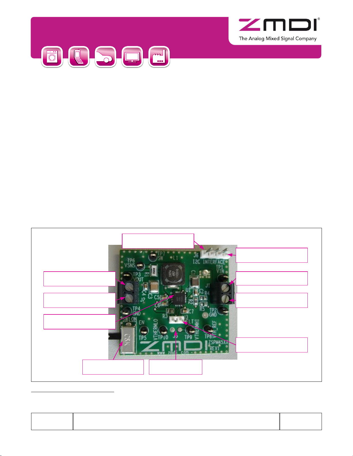
4.1. Board Connectors......................................................................................................................................7
4.2. Test and Probe Points...............................................................................................................................7
5Setup................................................................................................................................................................8
6Installing the Graphical User Interface (GUI) for the ZSPM4521.....................................................................8
7Installing Drivers for FTDI USB/ I2C™ Cable ...................................................................................................8
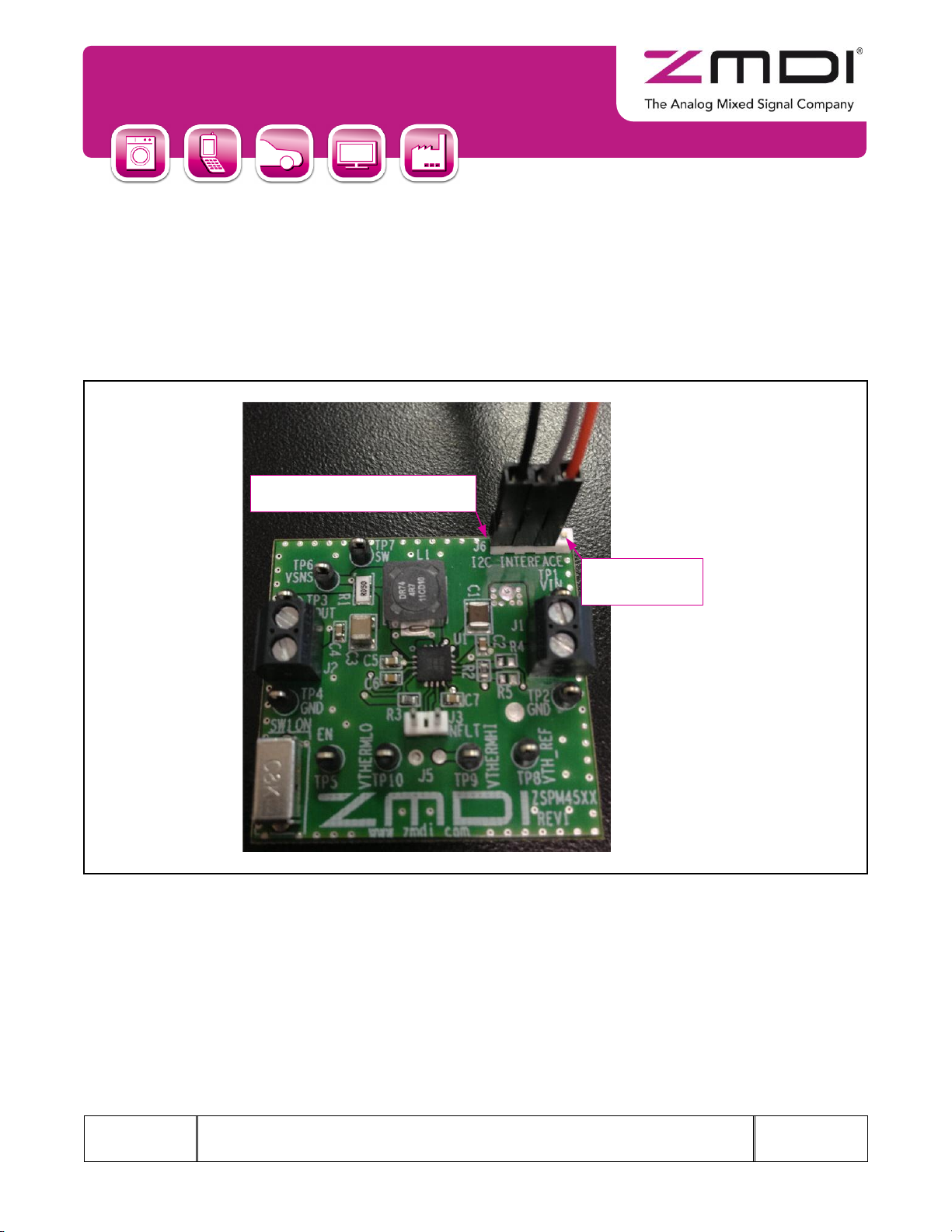
8Connecting the FTDI Cable to ZSPM4521 Eval Board:...................................................................................9
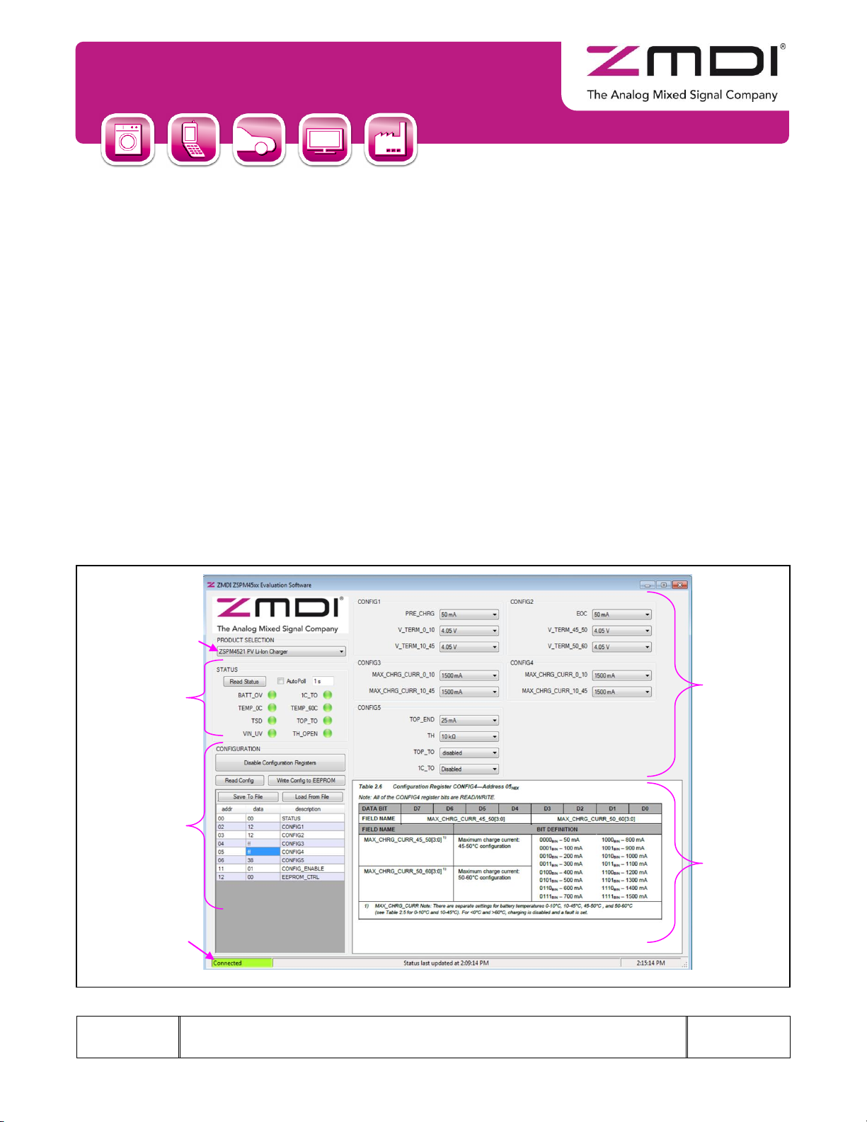
9I2C™ Programming GUI Overview.................................................................................................................10
9.1. Status Section..........................................................................................................................................11
9.2. Configuration and CONFIGx Sections ....................................................................................................12
9.3. Reference Section...................................................................................................................................13
10 Board Options ................................................................................................................................................14
10.1. Schottky Diode ........................................................................................................................................14
10.2. Zener Diode.............................................................................................................................................14
11 Evaluation Board Schematic and Layout.......................................................................................................14
11.1. Evaluation Board Layout .........................................................................................................................15
11.2. ZSPM4521 Evaluation Board Bill of Materials.........................................................................................16
12 Ordering Information ......................................................................................................................................17
13 Related Documents........................................................................................................................................17
14 Glossary .........................................................................................................................................................17
15 Document Revision History............................................................................................................................18

ZSPM4521
Evaluation Kit Manual
Kit Description
February 12, 2013
© 2013 Zentrum Mikroelektronik Dresden AG —Rev. 1.00
All rights reserved. The material contained herein may not be reproduced, adapted, merged, translated, stored, or used without the
prior written consent of the copyright owner. The information furnished in this publication is subject to changes without notice.
3 of 18
List of Figures
Figure 2.1 Overview of ZSPM4521 Evaluation Board ............................................................................................4
Figure 3.1 Charging State Diagram ........................................................................................................................6
Figure 8.1 Connecting the FTDI USB/ I2C™ Cable to J6 .......................................................................................9
Figure 9.1 The ZSPM4521 Graphic User Interface (GUI) ....................................................................................10
Figure 9.2 Reading Status Registers....................................................................................................................11
Figure 9.3 Fault Indication for Status Register Bits ..............................................................................................11
Figure 9.4 Enabling/Disabling...............................................................................................................................12
Figure 9.5 Buttons for Saving Current Configuration Settings or Loading Previously Saved Configurations ......13
Figure 9.6 Using the Reference Section in Conjunction with the Configuration Section......................................13
Figure 11.1 Schematic for the ZSPM4521 Evaluation Board Revision 1.0 ............................................................14
List of Tables
Table 11.1 ZSPM4521 Evaluation Board Bill of Materials.....................................................................................16

ZSPM4521
Evaluation Kit Manual
Kit Description
February 12, 2013
© 2013 Zentrum Mikroelektronik Dresden AG —Rev. 1.00
All rights reserved. The material contained herein may not be reproduced, adapted, merged, translated, stored, or used without the
prior written consent of the copyright owner. The information furnished in this publication is subject to changes without notice.
4 of 18
1 Kit Contents
ZSPM4521 Evaluation Board (EVB)
USB to I2C™
*
Cable
Startup Information
2 Introduction
The ZSPM4521 Evaluation Board (EVB) contains the ZSPM4521 High-Efficiency Photovoltaic Battery Charger
integrated circuit with recommended external components and test points (see Figure 2.1). The ZSPM4521
enables a complete battery charging system using a photovoltaic cell.
Key parameters of the battery charger are
Battery: lithium ion or lithium polymer, 3.7V rated cell
Photovoltaic voltage input: 4V to 7.2V
Important: Ensure that the power switch is in the off position (move to lower position when board is oriented as
shown in Figure 2.1) when connecting hardware as labeled on the EVB.
Figure 2.1 Overview of ZSPM4521 Evaluation Board
ZSPM4521 Pin 1
J1 Supply GND Input Post
Switch 1
(Power on = top position)
J6 Header for Accessing
SDA (pin 3) and SCL (pin 2)
J1 Supply VIN Input Post
Connect Battery’s Neg. Terminal
to J2 Terminal GND Post
Connect Battery’s Pos. Terminal
to J2 Terminal VOUT Post
J5 Footprint for Optional
Thermister Connector
Pin 1 on J6 has been removed
to prevent connection errors
J3, pin 2, to NFLT pin
on ZSPM4521
*
I2C™ is a trademark of NXP.

ZSPM4521
Evaluation Kit Manual
Kit Description
February 12, 2013
© 2013 Zentrum Mikroelektronik Dresden AG —Rev. 1.00
All rights reserved. The material contained herein may not be reproduced, adapted, merged, translated, stored, or used without the
prior written consent of the copyright owner. The information furnished in this publication is subject to changes without notice.
5 of 18
3 General Overview
3.1. Default Settings
The EVB is preset to have a 1.0A maximum charging current, 4.12V termination voltage, 100mA pre-charge
current, and 100mA end-of-charge current. These parameters are adjustable and can be customized to a specific
system optimization and stored in EEPROM memory through the I2C™
*
interface. With the default settings, the
charging current and termination voltage are independent of battery temperature. However, these parameters can
be set via EEPROM settings to automatically adjust based on the battery temperature in order to meet the JEITA
charging standard. Details of the I2C™ interface and register programming can be found in the ZSPM4521
datasheet.
The SDA and SCL nodes for I2C™communication are accessible via the J6 header pins (see Figure 2.1). If the
EVB’s default ZSPM4521 configuration settings are desired, no I2C™operation is needed.
Operating the ZSPM4521 EVB is straightforward. Once the Li-ion battery and input voltage are properly
connected as described in section 4.1, simply set switch SW1 to the ON position (see Figure 2.1), which starts the
charging of the battery.
*
I2C™ is a trademark of NXP.

ZSPM4521
Evaluation Kit Manual
Kit Description
February 12, 2013
© 2013 Zentrum Mikroelektronik Dresden AG —Rev. 1.00
All rights reserved. The material contained herein may not be reproduced, adapted, merged, translated, stored, or used without the
prior written consent of the copyright owner. The information furnished in this publication is subject to changes without notice.
6 of 18
Figure 3.1 Charging State Diagram
CONSTANT VOLTAGE MODE
FULL-CHARGE CONSTANT
CURRENT (CC) MODE
PRE-CHARGE STATE
INITIALIZE STATE
INITIALIZE
Waiting for Valid
Charging Conditions
NO
PRE-CHARGE
MPPT w/Pre-charge
Current Limit
VBAT > VPRECHG
Threshold
YES
NO
1C CHARGING
MPPT w/1C Current Limit and
Full Charge Timer
YES
No Faults &
VBAT < VRESTART
VBAT< VPRECHG
Threshold
VBAT =VTERMINATION
& ICHARGE < IEOC
YES
NO
YES
NO
END OF CHARGE
VBAT regulated to VTERMINATION
with EOC Timer
VBAT =
VTERMINATION
NO
YES
ICHARGE < Top Off
End Current
NO
EN
YES

ZSPM4521
Evaluation Kit Manual
Kit Description
February 12, 2013
© 2013 Zentrum Mikroelektronik Dresden AG —Rev. 1.00
All rights reserved. The material contained herein may not be reproduced, adapted, merged, translated, stored, or used without the
prior written consent of the copyright owner. The information furnished in this publication is subject to changes without notice.
7 of 18
4 Connectors and Test Points
4.1. Board Connectors
The board contains the following connectors for external signals and supplies:
J1: The input supply voltage for the board, which is controlled by the ZSPM4521 to charge the
battery.
J2: Output voltage from the charger.
J3: Pin 2 –Open drain output for the ZSPM4521’s NFLT pin (see ZSPM4521 data sheet for details).
J5: Battery temperature sensor / thermistor input (optional).
J6: I2C™ connector. Pin 4 is next to “J6 I2C” on ZSPM4521 Evaluation Board (Figure 2.1)
VDD –pin 1 (Note this pin has been removed to avoid erroneous connections that could damage
the board.)
SCL –pin 2
SDA –pin 3
GND –pin 4
4.2. Test and Probe Points
The board contains the following test/probe points:
TP3 (VOUT): Kelvin test point for VBAT+ (VOUT) to the positive battery terminal.
TP4 (GND): Kelvin test point for the negative battery terminal and ground for the EVB.
TP7 (SW): Switching node test point (SW pin on the ZSPM4521).
TP6 (VSNS): Sense voltage test point (VSENSE pin on the ZSPM4521).
TP5 (EN): Enable pin test point (EN pin on the ZSPM4521).
TP8 (VTH_REF): VTH_REF test point.
TP9 (VTHERMHI) / TP10 (VTHERMLO): Respectively, the positive and negative Kevin connection test
points for thermistor for measuring battery temperature.

ZSPM4521
Evaluation Kit Manual
Kit Description
February 12, 2013
© 2013 Zentrum Mikroelektronik Dresden AG —Rev. 1.00
All rights reserved. The material contained herein may not be reproduced, adapted, merged, translated, stored, or used without the
prior written consent of the copyright owner. The information furnished in this publication is subject to changes without notice.
8 of 18
5 Setup
Important: Follow these guidelines when connecting a DC input and battery to the ZSPM4521 Evaluation Board
(see Figure 2.1).
Battery: Connect the terminals of the battery to the EVB’s J2 terminal so that the “+” battery terminal is
connected to the J2 post marked “VOUT”and the “–” battery terminal is connected to GND of J2 (post
nearest test point TP4).
Supply: Connect the supply voltage to the Evaluation Board’s J1 terminal so that the positive rail is
connected to the J1 post marked “VIN” and the ground or negative rail is connected to GND of J1 (post
nearest test point TP2).
Battery Thermistor: The J5 connector is unpopulated by default so that the user can determine the type of
connection if using the battery thermistor feature. Connect the positive terminal of the thermistor for sensing
battery temperature to the Evaluation Board’s VTHERM HI connector on J5. Connect the negative terminal
of the thermistor to the board’s VTHERM LO connector on J5, which is also the common ground on the
board.
Important: Be sure to apply power to the ZSPM4521 EVB and set the EVB power switch to the “ON”
position prior to using the GUI.
6 Installing the Graphical User Interface (GUI) for the ZSPM4521
Follow these steps to create a user account on ZMDI’s website and download the GUI:
Go to www.ZMDI.com, and create a user name and login following instructions given on the site.
Place the cursor over the “PRODUCTS”tab, and select Smart Power Management from the drop-down
menu.
Click on ZSPM4521 on the secondary drop-down menu.
Under the “SOFTWARE” heading, click on “ZSPM45xx Programmer” to download the GUI as a zip file.
Next, extract the files in the downloaded ZIP file, and click on ZSPM45xx_Programmer.exe. Follow the installation
wizard to complete the installation.
7 Installing Drivers for FTDI USB/ I2C™ Cable
If using Windows® 7 or later, install the drivers for the FTDI USB/ I2C™ cable by simply connecting the cable to
the USB port on the computer and allowing the operating system to use Windows® Update to download and
install the required drivers.
If using an older version of Windows® or if the method above is unsuccessful for automatically installing the
drivers, refer to section 2.1 of the cable manufacturer’s datasheet for supported drivers and download
instructions:
http://www.ftdichip.com/Support/Documents/DataSheets/Cables/DS_C232HM_MPSSE_CABLE.PDF. This docu-
ment also provides a user guide for the cable.

ZSPM4521
Evaluation Kit Manual
Kit Description
February 12, 2013
© 2013 Zentrum Mikroelektronik Dresden AG —Rev. 1.00
All rights reserved. The material contained herein may not be reproduced, adapted, merged, translated, stored, or used without the
prior written consent of the copyright owner. The information furnished in this publication is subject to changes without notice.
9 of 18
8 Connecting the FTDI Cable to ZSPM4521 Eval Board:
Connect the female connector of the FTDI USB/ I2C™ cable to J6 of ZSPM4521 Evaluation Board being careful to
use the orientation shown in Figure 8.1. The order of the leads in the cable from left to right is black, gray, and
then orange. Note that the last pin on the right on J6 has been removed to ensure that no accidental connections
can be made, which would damage the board.
Figure 8.1 Connecting the FTDI USB/ I2C™ Cable to J6
Ensure that cable is connected flush with
left side of J6 with black lead to the left.
Pin 1 on J4 has been
removed to avoid
connection errors.

ZSPM4521
Evaluation Kit Manual
Kit Description
February 12, 2013
© 2013 Zentrum Mikroelektronik Dresden AG —Rev. 1.00
All rights reserved. The material contained herein may not be reproduced, adapted, merged, translated, stored, or used without the
prior written consent of the copyright owner. The information furnished in this publication is subject to changes without notice.
10 of 18
9 I2C™ Programming GUI Overview
ZSPM4521 GUI enables the user to communicate with the ZSPM4521 EVB, monitor status bits, and change
settings. It is also designed to accommodate all ZSPM45xx family ICs.
Upon activating the software, select “ZSPM4521 PV Li-Ion Charger” from the drop-down menu under “PRODUCT
SELECTION” (see Figure 9.1).
This GUI is divided into sections as shown in Figure 9.1:
The “Status” section allows reading the status registers for monitoring the ZSPM4521.
The “Configuration” and “CONFIGx” sections allow programming different parameters in the ZSPM4521.
The “Reference” section provides information from the datasheet showing definitions for programming
values for configurable registers in “Configuration” section. See section 9.3 for an explanation of which
register definitions will be displayed.
Note: At the bottom left of the GUI window, the status of communication of the USB to I2C™ interface is indicated.
The status should indicate “Connected” as shown in Figure 9.1 if the cable is connected to the computer. If the
GUI shows “Disconnected,” ensure that the I2C™/USB cable is connected to the computer and the driver is
installed; then try again. If there is a problem reading values from the GUI, verify that ZSPM4521 EVB is powered
on.
Figure 9.1 The ZSPM4521 Graphic User Interface (GUI)
CONFIG1 to
CONFIG5
Sections
Reference
Section
(Changes to
the register
selected)
Select
ZSPM4521
Configuration
Section
Status
Section
Connection
Status

ZSPM4521
Evaluation Kit Manual
Kit Description
February 12, 2013
© 2013 Zentrum Mikroelektronik Dresden AG —Rev. 1.00
All rights reserved. The material contained herein may not be reproduced, adapted, merged, translated, stored, or used without the
prior written consent of the copyright owner. The information furnished in this publication is subject to changes without notice.
11 of 18
9.1. Status Section
Click on the “Read Status”button to read the current values of monitor registers of the ZSPM4521 on the EVB.
Enabling the “Auto Poll” feature will automatically read the status bits at the time interval specified in the adjacent
field.
Figure 9.2 Reading Status Registers
Note: If any of the Status register bits shows a fault condition, the adjacent indicator is displayed as red as shown
in the figure below.
Figure 9.3 Fault Indication for Status Register Bits
Click “Read Status” button
to update status register
readings from ZSPM4521.
Check “Auto Poll” box to
continuously, automatically
update the status register
readings at the interval set
in the adjacent field.

ZSPM4521
Evaluation Kit Manual
Kit Description
February 12, 2013
© 2013 Zentrum Mikroelektronik Dresden AG —Rev. 1.00
All rights reserved. The material contained herein may not be reproduced, adapted, merged, translated, stored, or used without the
prior written consent of the copyright owner. The information furnished in this publication is subject to changes without notice.
12 of 18
9.2. Configuration and CONFIGx Sections
The recommended method for changing configuration settings is to select the required setting from each of the
drop-down menus for each register in the “CONFIG1” through “CONFIG5” sections at the top right of the GUI
shown in Figure 9.1. For advanced users who are knowledgeable in ZSPM4521 bit assignments (for details, refer
to ZSPM4521_Data_Sheet_rev_X_xy.pdf), settings can be changed manually using the “Configuration” section at
the bottom left of the GUI.
The “Configuration” section of the GUI enables changing the hexadecimal data settings in the configurable
registers of the ZSPM4521 (except STATUS, which is read-only). To change the registers, click on the “Enable
Configuration Registers” button as shown in Figure 9.4. To prevent further changes to the configuration registers,
click “Disable Configuration Registers.”After enabling configuration of the registers, click on the “Read Config”
button to read the current configuration of the ZSPM4521.
Recommendation: Record the existing configuration register settings before changing any settings and writing the
new configuration to the ZSPM4521. Refer to the “Reference” section (see section 9.3) for definitions for the
register bits and valid settings.
Option: The “Load from File” button can be used to select a pre-defined set of values for the configuration
registers from a previously saved configuration file (see Figure 9.5).
Figure 9.4 Enabling/Disabling
Default Condition = Disabled
Configuration Registers are Write-Protected
Writing to Configuration
Registers is Enabled
To change a register manually, click on the row for the register and enter the new value for the register in
hexadecimal as illustrated in Figure 9.6.
Click to Enable Writing to
Configuration Registers

ZSPM4521
Evaluation Kit Manual
Kit Description
February 12, 2013
© 2013 Zentrum Mikroelektronik Dresden AG —Rev. 1.00
All rights reserved. The material contained herein may not be reproduced, adapted, merged, translated, stored, or used without the
prior written consent of the copyright owner. The information furnished in this publication is subject to changes without notice.
13 of 18
Important: After changing the configuration of the registers as needed, the values entered will take effect
immediately, but values will not be stored in the EEPROM. The values will be lost after a power cycle. In order to
write the configuration to the EEPROM, click the “Write Config to EEPROM” button to write the new values to
ZSPM4521’s EEPROM configuration registers.
The GUI provides the “Save to File” button for saving the current configuration to a file, so that the user has the
option to load the file in the future using the “Load From File” button.
Figure 9.5 Buttons for Saving Current Configuration Settings or Loading Previously Saved Configurations
9.3. Reference Section
The right panel of the GUI provides a reference from the datasheet showing the definitions for register bits.
By default, the Status register definitions are shown as illustrated in Figure 9.1.
When access to the configuration registers has been enabled (see section 9.2), the “Reference” section provides
defined values for configuration options for the register selected in the “Configuration” section.
Figure 9.6 Using the Reference Section in Conjunction with the Configuration Section
Reference
Section
(Changes to
the register
selected)
Configuration
Section
3. Click on the row of the
register to be revised.
4. Refer to the data sheet definitions for the
register bits in the selected row and enter the
new hexadecimal value in the “data” column.
1. Click here if needed to display
“Disable Configuration Registers”
(enables writing to configurable
registers).
2. Then click “Read Config.”

ZSPM4521
Evaluation Kit Manual
Kit Description
February 12, 2013
© 2013 Zentrum Mikroelektronik Dresden AG —Rev. 1.00
All rights reserved. The material contained herein may not be reproduced, adapted, merged, translated, stored, or used without the
prior written consent of the copyright owner. The information furnished in this publication is subject to changes without notice.
14 of 18
10 Board Options
Refer to the bill of materials in section 11.2 for recommended values and sources for the following optional com-
ponents.
10.1. Schottky Diode
While D1 is not required, it can be populated to increase efficiency and provide a better load regulation. Care
should be taken to select a diode that is rated to handle the output current supplied by the regulator.
10.2. Zener Diode
Zener diodes, D2 and D3, are not populated. However, adding D2 or D3 is highly recommended to protect the
ZSPM4521 by clamping the input voltage to the maximum input voltage of 7.2V.
11 Evaluation Board Schematic and Layout
Figure 11.1 Schematic for the ZSPM4521 Evaluation Board Revision 1.0

ZSPM4521
Evaluation Kit Manual
Kit Description
February 12, 2013
© 2013 Zentrum Mikroelektronik Dresden AG —Rev. 1.00
All rights reserved. The material contained herein may not be reproduced, adapted, merged, translated, stored, or used without the
prior written consent of the copyright owner. The information furnished in this publication is subject to changes without notice.
15 of 18
11.1. Evaluation Board Layout
Top Layer
2nd Layer
3rd Layer
Bottom Layer

ZSPM4521
Evaluation Kit Manual
Kit Description
February 12, 2013
© 2013 Zentrum Mikroelektronik Dresden AG —Rev. 1.00
All rights reserved. The material contained herein may not be reproduced, adapted, merged, translated, stored, or used without the
prior written consent of the copyright owner. The information furnished in this publication is subject to changes without notice.
16 of 18
11.2. ZSPM4521 Evaluation Board Bill of Materials
Table 11.1 ZSPM4521 Evaluation Board Bill of Materials
Reference
Part
Footprint
Manufacturer
Manufacturer P/N
C1
10µF/16V
1210
TDK
C3225Y5V1C106Z/1.15
C2
0.1µF/25V
603
Murata
GRM188R71C104KA01D
C4
0.1µF/25V
603
C5
0.1µF/25V
603
C6
0.1µF/25V
603
C7
0.1µF/25V
603
C3
4.7µF/25V
1210
TDK
C3225X7R1E475K
D1
DIODE SCHOTTKY
smc_smb
NL
D2
DIODE ZENER
do201ad
NL
D3
DIODE ZENER
smc_smb
NL
J1
VIN
OSTVQ021150
On Shore Technology
ED555/2DS
J2
VOUT
OSTVQ021150
On Shore Technology
ED555/2DS
J3
HEADER 2
jumper2
TE Connectivity
3-644456-2
J5
VTHERM
jumper2
NL
J6
I2C™ Bus
jumper4
TE Connectivity
3-644456-4
L1
4.7µH
ind
Cooper Bussman
DR74-4R7-R
R1
50mΩ/1W/1%/50ppm
1206
Ohmite
MCS1632R050FER
R2
10K
603
Stackpole
RMCF0603JT10K0
R3
1k
603
Stackpole
RMCF0603JT1K00
R4
NL
603
NL
R5
NL
603
NL
SW1
SW_T_SPDT
OS102011MA1QN1
C&K
OS102011MA1QN1
TP1
VIN
TP
Keystone
5001K-ND
TP2
GND
TP
Keystone
5001K-ND
TP4
GND
TP
Keystone
5001K-ND
TP3
VOUT
TP
Keystone
5001K-ND
TP5
EN
TP
Keystone
5001K-ND
TP6
VSNS
TP
Keystone
5001K-ND
TP7
SW
TP
Keystone
5001K-ND

ZSPM4521
Evaluation Kit Manual
Kit Description
February 12, 2013
© 2013 Zentrum Mikroelektronik Dresden AG —Rev. 1.00
All rights reserved. The material contained herein may not be reproduced, adapted, merged, translated, stored, or used without the
prior written consent of the copyright owner. The information furnished in this publication is subject to changes without notice.
17 of 18
Reference
Part
Footprint
Manufacturer
Manufacturer P/N
TP8
VTH_REF
TP
Keystone
5001K-ND
TP9
VTHERMHI
TP
Keystone
5001K-ND
TP10
VTHERMLO
TP
Keystone
5001K-ND
U1
ZSPM4521
pqfn-16
ZMDI
ZSPM4521
12 Ordering Information
Product Sales Code
Description
ZSPM4521KIT
ZSPM4521 Evaluation Kit for the ZSPM4521 High Efficiency Photovoltaic Charger for Li-
ion Battery
13 Related Documents
Note: X_xy refers to the latest version of the document.
File Name
File Name
ZSPM4521 Datasheet
ZSPM4521_Data_Sheet_rev_X_xy.pdf
Visit ZMDI’s website www.zmdi.com or contact your nearest sales office for the latest version of these documents.
14 Glossary
Term
Description
JEITA
Japan Electronics and Information Technology Industries Association

ZSPM4521
Evaluation Kit Manual
Kit Description
February 12, 2013
© 2013 Zentrum Mikroelektronik Dresden AG —Rev. 1.00
All rights reserved. The material contained herein may not be reproduced, adapted, merged, translated, stored, or used without the
prior written consent of the copyright owner. The information furnished in this publication is subject to changes without notice.
18 of 18
15 Document Revision History
Revision
Date
Description
1.00
February 12, 2013
First release.
Sales and Further Information www.zmdi.com Analog@zmdi.com
Zentrum Mikroelektronik
Dresden AG
Grenzstrasse 28
01109 Dresden
Germany
ZMD America, Inc.
1525 McCarthy Blvd., #212
Milpitas, CA 95035-7453
USA
Zentrum Mikroelektronik
Dresden AG, Japan Office
2nd Floor, Shinbashi Tokyu Bldg.
4-21-3, Shinbashi, Minato-ku
Tokyo, 105-0004
Japan
ZMD Far East, Ltd.
3F, No. 51, Sec. 2,
Keelung Road
11052 Taipei
Taiwan
Zentrum Mikroelektronik
Dresden AG, Korea Office
U-space 1 Building
11th Floor, Unit JA-1102
670 Sampyeong-dong
Bundang-gu, Seongnam-si
Gyeonggi-do, 463-400
Korea
Phone +49.351.8822.7.776
Fax +49.351.8822.8.7776
Phone +855.275.9634 (USA)
Phone +408.883.6310
Fax +408.883.6358
Phone +81.3.6895.7410
Fax +81.3.6895.7301
Phone +886.2.2377.8189
Fax +886.2.2377.8199
Phone +82.31.950.7679
Fax +82.504.841.3026
DISCLAIMER: This information applies to a product under development. Its characteristics and specifications are subject to change without notice. Zentrum Mikroelektronik Dresden AG
(ZMD AG) assumes no obligation regarding future manufacture unless otherwise agreed to in writing. The information furnished hereby is believed to be true and accurate. However, under
no circumstances shall ZMD AG be liable to any customer, licensee, or any other third party for any special, indirect, incidental, or consequential damages of any kind or nature whatsoever
arising out of or in any way related to the furnishing, performance, or use of this technical data. ZMD AG hereby expressly disclaims any liability of ZMD AG to any customer, licensee or
any other third party, and any such customer, licensee and any other third party hereby waives any liability of ZMD AG for any damages in connection with or arising out of the furnishing,
performance or use of this technical data, whether based on contract, warranty, tort (including negligence), strict liability, or otherwise.
Table of contents