Acqiris U5310A User manual

Acqiris U5310A
Acquisition Card
2 channels, 10-bit, from 5 to 10 GS/s,
DC up to 2.5 GHz bandwidth, with real-time processing
User's Manual

2 U5310A User's Manual
Copyright Statement
© Acqiris, 2017 - 2019
No part of this manual may be reproduced in any form or by any means (including electronic storage
and retrieval or translation into a foreign language) without prior agreement and written consent from
Acqiris SA as governed by international copyright laws.
Version
July 2019
Contact us
Acqiris Americas
contact-americas@acqiris.com
Acqiris Europe
contact-emea@acqiris.com
Acqiris Asia-Pacific
contact-asia-pacific@acqiris.com
Acqiris Japan
contact-japan@acqiris.com
Worldwide contact for support
support@acqiris.com
Acqiris SA
Chemin des Aulx, 12
1228 Plan-Les-Ouates
Switzerland
www.acqiris.com

U5310A Acquisition Card User's Manual
U5310A User's Manual 3
U5310A Acquisition Card User's Manual
This help document is intended to provide in-depth information and reference material specific to your
ADC Card.
For information about installation and about getting started with your ADC Card, please refer to the
Startup Guide which can be downloaded from https://extranet.acqiris.com/ or which is installed with
your software.
Content
U5310A Acquisition Card User's Manual 3
Content 3
Introduction 5
Overview 5
Product description 5
Main ADC Card Features 7
1.1 U5310A front panel features 8
1.2 Channel Input Specifications 9
1.3 Sampling and Data Acquisition 11
1.4 Trigger 12
1.5 Calibration 14
Real-Time Processing Options 16
2.1 Easy firmware switch 16
2.2 Digitizer firmware (DGT option) 17
2.3 Real-time averaging (AVG option) 20
Readout modes 30
3.1 Standard readout modes 30
3.2 Continuous Simultaneous acquisition and readout, with trigger (CST option) 31
Other Signal Processing Features 39
4.1 Sampling rate reduction (binary decimation) 40
4.2 Equalization 41
Control and Synchronization 48
5.1 External clock and reference 49
5.2 Trigger modes and time-stamps 50
5.3 Trigger output 53
5.4 Multi-purpose inputs and outputs 56
Programming Information 58
6.1 Overview of the AqMD3 Driver 58

Content
4 U5310A User's Manual
6.2 Programming with the IVI-C Driver in various development environments 59
6.3 Migrating from MD2 2.x to MD3 3.x 61
6.4 Initial configuration 62
6.5 Apply setup 63
How To ... ? 64
7.1 How to discover the PXI Instrument? 65
7.2 How to calibrate the card? 66
7.3 How to configure and read data on two channels? 70
7.4 How to access repeated capabilities? 71
7.5 How to generate a software trigger? 72
7.6 How to perform time-interleaving acquisitions? 73
7.7 How to enable or bypass the bandwidth limiter? 74
7.8 How to set the external trigger? 75
7.9 How to perform binary decimation? (depending on firmware) 76
7.10 How to perform partial readout? 77
7.11 How to load a new firmware? 80
7.12 How to switch from normal mode acquisition (Multi-record) to averager mode? 81
Software utilities 82
8.1 ADC card Verification Utility (AqMD3Verify) 82
FAQ 84
9.1 Q. What is coherent sampling? 84
9.2 Q. How to manage the internal temperature? 84
9.3 Q. What are the differences between the various data streaming firmware options supported
by high-speed ADC cards ? 85
9.4 Q. What happens if the host processor goes in hibernation mode? 86
General information 87
10.1 Safety notes 87
10.2 Cleaning precautions 89
10.3 Product markings 89
10.4 Electrical &environmental specifications 90
10.5 Related documentation 90
10.6 Full product family 91
Introduction
U5310A User's Manual 5
Introduction
Overview
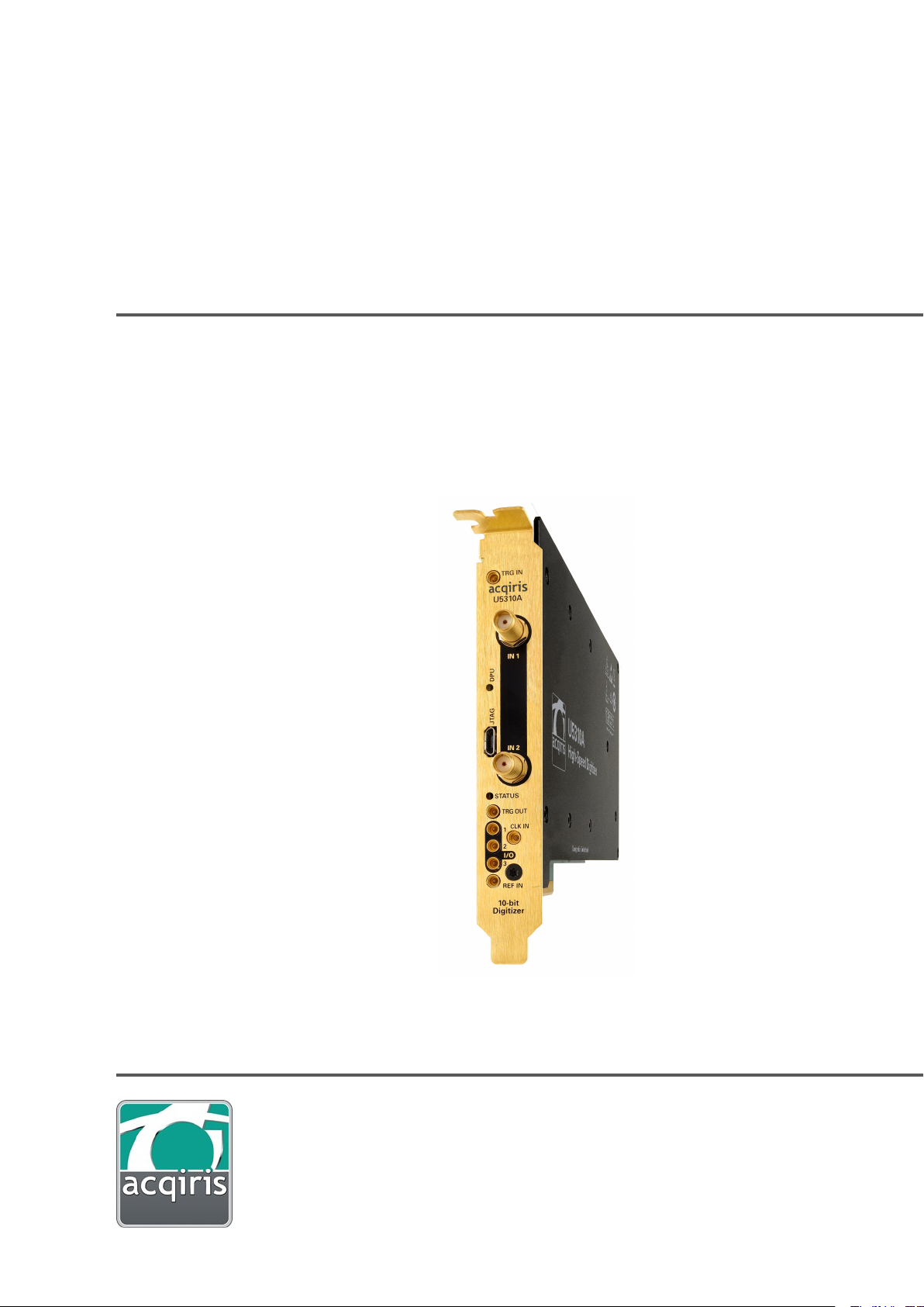
The U5310A is a true two channel PCIe, DC coupled 10-bit signal acquisition card providing sample
rates up to 10 GS/s with 2.5 GHz bandwidth.
The U5310A PCIe ADC card is particularly suited for embedded OEM applications requiring digitizer
sampling at wide bandwidth and moderate dynamic range. Overall performance enables customer's
final products to more precisely measure time of flight for a variety of end system applications.
Product description
The U5310A ADC card occupies a single full-length PCIe slot of the host PC. Featuring sample rates
of up to 5 GS/s per channel, up to 10 GS/s in interleaved mode (-INToption), along with an analog
bandwidth of up to 2.5 GHz and DDR3 acquisition memory options up to 4 GB, the U5310A includes a
Xilinx Virtex-6 FPGA for real-time processing.
The U5310A-CH1 version allows to acquire signal on a single channel at 5 GS/s.
The standard digitizer firmware included allows signal acquisition to the on-board memory and
subsequent transfer to the host PC via its PCI Express 2.0 eight lanes connection.
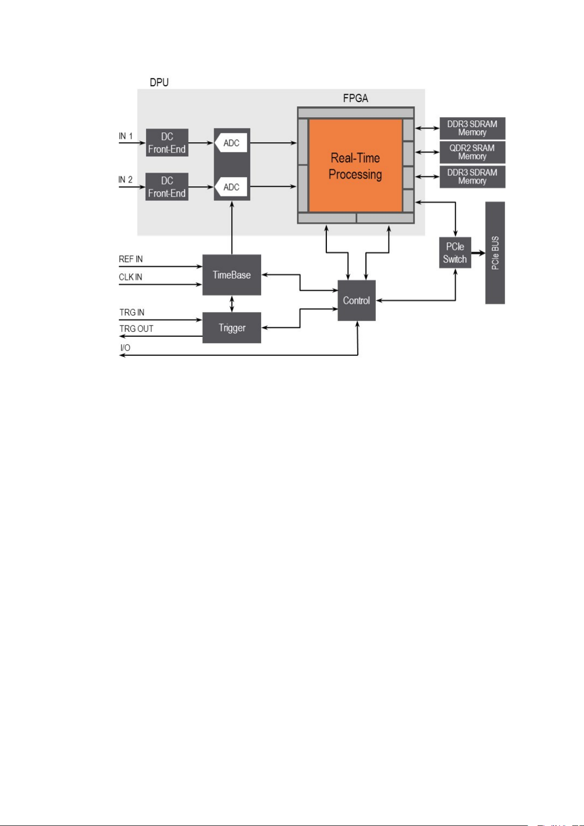
At the heart of the U5310A is a data processing unit (DPU) based on the powerful Xilinx Virtex-6
FPGA. This DPU is responsible for controlling the module functionality, data flow and real-time signal
processing. This powerful feature allows data reduction and storage to be carried out at the ADC card
level, minimizing transfer volumes and speeding-up analysis.

Product description
6 U5310A User's Manual
Figure 1.1 - U5310A, dual channel version block diagram.
Most of the technical specifications concerning your particular ADC card are covered in this manual,
however for the complete specifications please refer to the product's from www.acqiris.com.

1.1 U5310A front panel features
8 U5310A User's Manual
1.1 U5310A front panel features
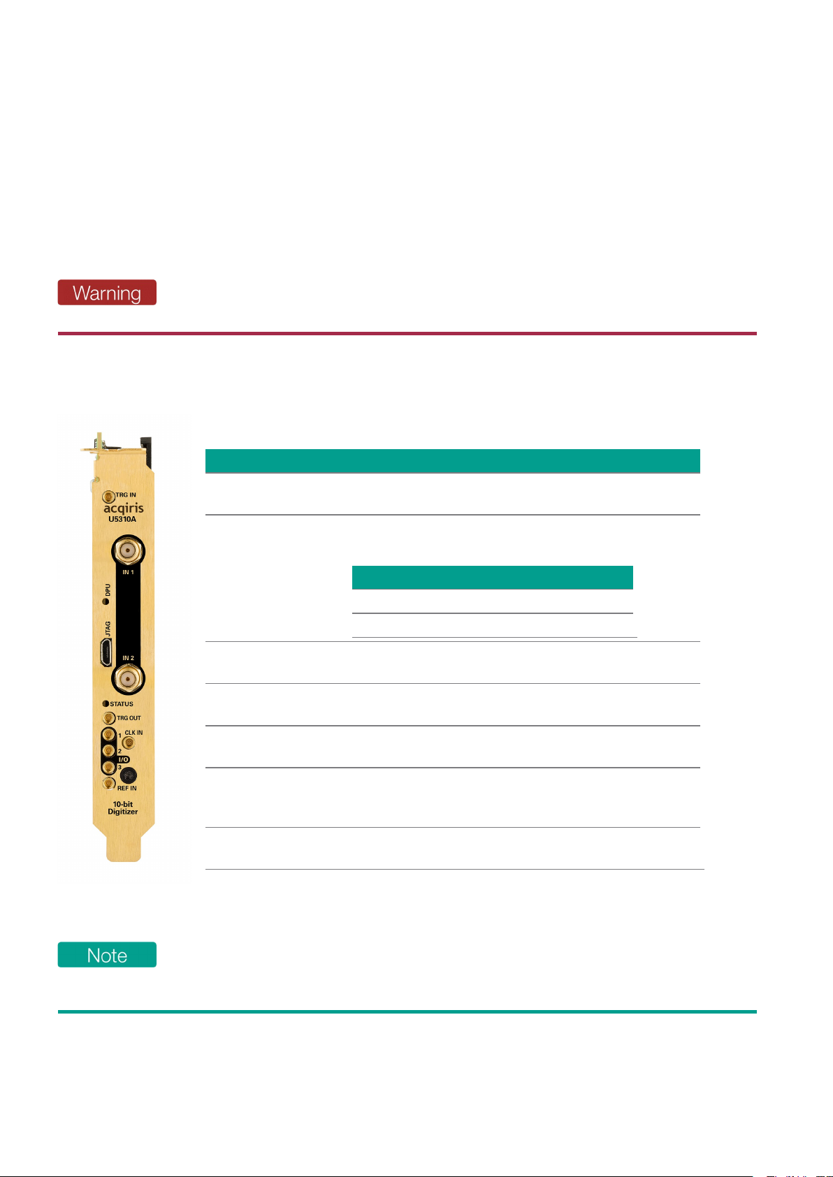
Front panel connectors
Please note that analog Input IN 1 and IN 2 have a maximum voltage limitation of ±1.5
Vmax while using the default 1V full scale range (±0.5 Vmax if using 0.25V FSR).
Connector Type Description
TRG IN MMCX
female External trigger input, 50 Ω DC terminated, ±5 V range.
IN 1, 2 SMA
female
Analog signal inputs, DC-coupled and 50 Ω terminated.
The input full scale ranges are selectable:
Range Maximum Input
0.25 V ±0.5 Vmax
1 V ±1.5 Vmax
JTAG Micro
USB Providesconnection to the DPU for specific reprogramming.
TRGOUT MMCX
female Trigger Out signal. User selectable from several functions.
I/O 1, 2, 3 MMCX
female
User configurable Input / Output signal. 3.3 V CMOS and
TTLcompatible.
CLK IN MMCX
female
External clock input. AC coupled and 50 Ω terminated, signal level: +5
to +15 dBm. (Please refer to U5310A datasheet for supported fre-
quency values).
REF IN MMCX
female
External reference clockinput, AC coupled and 50 Ω terminated. It can
accept a 100MHzsignal from -3 to +3 dBm.
Table 1.1 - List of U5310A front-panel IOs.
The ADC card can usually work with signals present at the external reference and clock inputs
(REF IN and CLK IN). However, to ensure the best performance, or if the calibration is found to be
unreliable, it is recommended to remove such signals when working with internal clock.

1.2 Channel Input Specifications
U5310A User's Manual 9
1.2 Channel Input Specifications
This section provides information and specifications regarding the input characteristics of the ADC
card.
Two channel versions exist for this 10-bit DC-coupled ADC card:
The U5310A-CH2 provides two 5 GS/s channels. The two channels may be combined to form
an interleaved channel at 10 GS/s (U5310A-INT option).
The U5310A-CH1 provides a single 5 GS/s channel1.
Channel Input
The U5310A has the following front end capabilities:
Coupling / Impedance Full Scale Ranges (FSR) Maximum operating voltage Input voltage offset
DC / 50 Ω
250 mV ± 0.5 V ± FSR
1 V ± 1.5 V ± FSR
Table 1.2 - Channel input specifications.
It is also possible to optimize the calibration for a specified target voltage. For details, see
Calibration optimized for a target voltage (page 66).
Impedance & Coupling
The input channel termination is 50Ω. The input coupling is DC.
Input Protection
The input amplifiers are designed to accept signals below the absolute maximum level shown in the
table.
Mezzanine Front-end
The front-end electronics are all mounted on a removable mezzanine card. In the event of accidental
damage or as components fatigue over time (e.g. relays in high duty cycle automated testing
applications), the mezzanine card allows for fast and efficient replacement.
1It is not possible with the -CH1 version to interleave channels and double the sampling rate. Only 5 GS/s is supported.

1.2 Channel Input Specifications
10 U5310A User's Manual
Bandwidth and Rise Time
The bandwidth specification indicates the frequency at which an input signal will be attenuated by 3dB
(approximately 30 % loss of amplitude).
The U5310A ADC card offers a 2 GHz bandwidth limiter -also see How to enable or bypass the
bandwidth limiter? (page 74).
The bandwidth also has an impact on the minimum rise and fall times that can be passed through the
front-end electronics. A pulse with a very sharp edge will be observed to have a minimum rise timeTmin
determined by the front-end electronics. In general a pulse with a given 10-90% rise time T10-90real will
be observed with a lower value given by:
T10-902=T10-90real2+Tmin2
where Tmin(ns)≈0.35/BW(GHz).
Using Bandwidth Limiter
U5310A ADC cards offer a 2 GHz bandwidth limiter capability (Specified with default mode
"Equalization Off").
Also see Programing section >How to enable or bypass the bandwidth limiter? (page 74).
When using the bandwidth limiter, it is recommended to use the default equalization mode
(Equalization off).
Vertical Resolution
The U5310A ADC Card uses 10-bit ADCs giving 1024 levels at each input full scale range.

1.3 Sampling and Data Acquisition
U5310A User's Manual 11
1.3 Sampling and Data Acquisition
The ADC Card acquires waveforms in association with triggers. Each waveform is made of a series of
measured voltage values (sample points) coming from the ADC at a uniform sampling rate.
Sampling rate
The U5310A Acquisition card contains an analog-to-digital conversion (ADC) system that can sample
waveforms, in a real time sampling mode, at the maximum rates shown in the table below. The
maximum sampling rate shown above is achieved by combining the two channels (-CH2/INT version).
Model Option Max. Sampling Rate Available Channels Resolution Acquisition Modes
U5310A
-SR4 5 GS/s 2
10 bits Single or multi-record
(up to 131'072 records)
-SR4 and INT 10 GS /s 1
Table 1.3 - Acquisition sampling rate and resolution per channel.
The External Clock can be used to vary the sampling rate of the ADC card, see External clock and
reference (page 49).
Combining channels (Interleaving -INT option)
When ordered with -INT option, the U5310A ADC card supports the capability of combining the
converters (and their memories) from two channels to analyze a single input channel. With this feature
the maximum sampling rate and the maximum amount of acquisition memory are doubled.

1.4 Trigger
12 U5310A User's Manual
1.4 Trigger
The trigger settings applied to the ADC card are used to determine at which time the device will start
recording data. The various trigger settings are outlined below.
Trigger source
The trigger source can be:
the signal applied to an input channel (internal triggering)
an external signal applied to the TRG IN front panel input connector (external triggering)
a software trigger (See How to generate a software trigger? (page 72)).
The different trigger modes are detailed in section Trigger modes and time-stamps (page 50)
Trigger impedance & coupling
The U5310A has a fixed 50 Ω termination impedance with DC coupling.
Trigger input bandwidths
The bandwidth depends on the trigger source.
Channel trigger
The -3 dB bandwidth of the comparator of the channel triggers is from DC to 2.6 GHz. For input signals
with high frequency components, this means that the signal acquired and displayed doesn’t
correspond exactly to the signal seen from the trigger comparator input. Since, the signal seen on the
trigger comparator can be attenuated, this should be taken into account when selecting channel
triggers and specifying the trigger level.
External trigger
The external trigger input has a bandwidth from DC to 2 GHz.
Refer to section How to set the external trigger? (page 75) for additional information.
Trigger level
The trigger level specifies the voltage at which the selected trigger source will produce a valid trigger.
All trigger circuits have sensitivity levels that must be exceeded in order for reliable trigger to occur.
The external trigger input and channel triggers have a hysteresis of 5% and 4% of FSR, respectively
(where FSR is the channel Full Scale Range).
On the external trigger, the Full Scale Range FSR is ±5 V, therefore the ADC card will trigger on
signals with a peak-to-peak amplitude > 0.5 V.
When using the channel triggers, the trigger level must be set within Offset ± (0.75 x FSR).

1.4 Trigger
U5310A User's Manual 13
Edge trigger slope
The trigger slope defines which one of the two possible transitions will be used to initiate the trigger
when it passes through the specified trigger level. Positive slope indicates that the signal is
transitioning from a lower voltage to a higher voltage. Negative slope indicates the signal is
transitioning from a higher voltage to a lower voltage.
Trigger precision and resolution
The U5310A trigger time interpolator offers a resolution of 6 to 8 ps (nominal) and a precision of 15 ps
RMS (nominal) .
If comparing the initial trigger time T0 measured using the same waveform either used as channel
input trigger or as an external trigger, the T0 position can be slightly different (especially if the
waveform used as trigger has a slow edge).
First, the analog bandwidth can be different for the channel trigger input and the external trigger
input, resulting in a different slope and so a different T0.
Secondly, compared with the channel trigger, the external trigger threshold is not calibrated. The
input channel trigger calibration allows a T0 adjustment both in threshold and in timing, resulting in a
more accurate T0. However, when using the external trigger, the measured T0 is still precise and
theT0 position difference stays stable.
Using a signal with faster edge as external trigger can reduce this effect.
Trigger delays
For more details about triggers modes, post/pre-trigger delays and time-stamps, see Trigger modes
and time-stamps (page 50).

1.5 Calibration
14 U5310A User's Manual
1.5 Calibration
The U5310A is factory calibrated and shipped with a calibration certificate.
The internal calibration refers to the adjustment of ADC card internal parameters, corresponding to
user selected parameters and required before starting acquisition.
Internal calibration
The internal calibration (or self-calibration) measures and adjusts the internal timing, gain and offset
parameters between the ADCs and against a precise reference.
The ADC card includes a high precision voltage source and a 16-bit DAC, used to perform the input
voltage and offset calibration.
The supplied software drivers include self-calibration function which can be executed upon user
request. The ADC cards are never self-calibrated in an automatic way, (i.e. as a consequence of
another operation). This ensures programmers have full control of all calibration operations performed
through software in order to maintain proper event synchronization within automated test applications.
For accurate time and voltage measurements it is recommended to perform a self-calibration once
the module has attained a stable operating temperature (usually reached after 20 minutes of ADC
card operation after power on).
A full internal calibration of a ADC card can be time consuming because of the many possible
configuration states. Therefore, the self-calibration is performed only for the current configuration
state, and is mandatory before making the first acquisition with given settings. Indeed the AqMD3
driver prevents an acquisition from being performed unless a self-calibration has first been completed.
Note that some configuration changes do not require a new self-calibration. To avoid unnecessary
self-calibrations, the IAqMD3Calibration.IsRequired IVI.NETproperty or the AQMD3_ATTR_
CALIBRATION_IS_REQUIRED IVI-C attribute should be queried.
ADC card can usually work with signals present at the channel input, or trigger input. However, to
ensure the best performance, or if the calibration is found to be unreliable (as shown by a calibration
failure status), it is recommended to remove such signals.
Similarly, when working with internal clock, it is recommended to remove external reference and
external clock inputs during calibration to avoid parasitic effects.
It is not recommended to perform multiple successive calibrations. If a recurrent calibration failure
occurs, in case of specific application, please contact support for advice.
Smart-calibration
The smart calibration implemented in MD3 drivers allows to save time by automatically keeping in
memory the calibration information from any self-calibration performed since the beginning of the
session. When the acquisition parameters are changed, no re-calibration of the card is necessary if a

1.5 Calibration
U5310A User's Manual 15
self-calibration has already been performed with the same acquisition conditions (i.e. the same set of
parameters), unless the clock mode parameters are changed.
Indeed, any change in the clock mode parameters (i.e. External clock frequency, Clock source or
Reference mode parameters), induces a restart of the clocks which requires a new self-calibration.
For details, see Parameter change requiring a new self calibration (page 67).
Calibration optimized for a target voltage
It is possible to optimize the calibration for a specified target voltage. In this case, the self-calibration
will minimize the noise level at the channel input value equal to this specified target voltage. For
details, see Calibration optimized for a target voltage (page 66).
Factory calibration
Factory calibration is the process of measuring the actual performance of a device-under-test (DUT)
using laboratory instruments that have significantly better performance than the DUT. Laboratory
instrument performance must be traceable to the International System (SI) Units via a national
metrology institute (NIST, NPL, NRC, PTB, CENAM, INMETRO, BIPM, etc.)
The measured performance is then compared to published datasheet specifications. For each factory
calibration, Acqiris tests the performance corresponding to all datasheet specifications, for every
installed option. If needed, the DUT is adjusted and re-qualified ; ensuring it is in line with full
specifications.
Our ADC cards are calibrated at factory during the production phase. There is no need to
systematically calibrate each year.
Firstly, the cards include a self-calibration function providing a good degree of confidence that your
card is operating within its specifications on a day-to-day basis, and triggering an error message if out
of calibration relative to the internal calibration signal.
Secondly, our cards are warranted to stay within specification over the standard 3-year warranty. They
usually stay within specification much longer and we rarely have to effectively recalibrate the cards.
Lastly, a onetime calibration can be ordered in case customer detects a deviation in the measure of its
final product that appears to be caused by the ADC card. The onetime calibration consists in
processing the card through production test to determine if it is still within specification:
If yes, the ADC card is returned with the certificate of calibration which certifies it is within spe-
cification.
If not, the required calibration is performed, and another production test is done to provide the
certificate of calibration.
If repair is required, and the card is out of warranty, a repair quote will be provided.
For more information, or to request for a calibration, please contact technical support
support@acqiris.com.

Real-Time Processing Options
16 U5310A User's Manual
Chapter 2
Real-Time Processing Options
The U5310A ADC Card provides several optional modes. This section describes each acquisition
mode and associated real-time signal processing.
2.1 Easy firmware switch 16
2.2 Digitizer firmware (DGT option) 17
2.3 Real-time averaging (AVG option) 20
The modes available with your product depends on the firmware options ordered with your products.
To check which options and mode are present on your ADC card you can use the MD3 Software
Front Panel from the: Windows Start Menu > Acqiris > MD3 > Acqiris MD3 SFP. Then use the
menu Help > About. The field System Options gives the option list.
2.1 Easy firmware switch
A simple call to the configuration function will enable to switch to the required option.

2.2 Digitizer firmware (DGT option)
U5310A User's Manual 17
2.2 Digitizer firmware (DGT option)
The digitizer firmware (normal mode) allows standard data acquisition, including: ADC card
initialization, setting of the acquisition and clocking modes, management of channel triggering for best
synchronization, storing data in the internal memory and/or transferring them to the host computer.
Single and multi-record acquisition modes
To maximize sampling rates and utilize memory as efficiently as possible the ADC cards include both
single and multi-record modes. For both of these modes the data of all of the active channels is
acquired synchronously; all of the ADC's are acquiring data at the same time, to within a small fraction
of the maximum sampling rate.
The single record acquisition mode is the normal operation of most ADC card products. In this
mode an acquisition consists of a waveform recorded with a single trigger. The user selects the
sampling rate and record size, and sets the number of records to 1 (default value). For details about the
trigger sources, see Trigger (page 12).
Figure 2.1 - Acquisition sequence using a single record.
The ADC cards also feature a multi-record acquisition mode. This mode allows the capture and
storage of consecutive single waveforms. Multi-record acquisition mode is useful as it can optimize
the ADC card's sampling rate and memory requirements for applications where only portions of the
signal being analyzed are important. The mode is extremely useful in almost all impulse-response type
applications (RADAR, SONAR, LIDAR, Time-of-Flight, Ultrasonics, Medical and Biomedical
Research, etc.).
In multi-record acquisition mode the acquisition memory is divided into a pre-selected number of
records. Waveforms are stored in successive memory records as they arrive. Each waveform requires
its own individual trigger.
Figure 2.2 - Acquisition sequence using a multi-records. It is possible to miss a trigger at high trigger rate, as
illustrated with trigger 3.

2.2 Digitizer firmware (DGT option)
18 U5310A User's Manual
The multi-record acquisition mode enables successive events, occurring within a very short time,
to be captured and stored without loss. A very fast trigger rearm time is a crucial feature for multi-
record acquisitions. Thanks to fast trigger rearm, the U5310A achieves very low “dead time” between
the records of a multi-record acquisition. The “dead time” is the period after the end of an event when
the card cannot accept a new trigger event. The re-arm time is provided in the U5310A's U5310A
datasheet.
Program examples for Single record or multi-records acquisitions are available:
For IVI-C C1:\Program Files\IVI Foundation\IVI\Drivers\AqMD3\Examples\IVI-C
For IVI.NET C:\Program Files\IVI Foundation\IVI\Drivers\AqMD3\Examples\IVI.NET
Acquisition memory
Data from the ADC is stored in on-board acquisition memory. The amount of memory in use for
acquisition can be programmed and is selectable from 1 point to the full amount of acquisition memory
available.
Model Memory option
ordered Acquisition memory Max samples/channel
U5310A
-M02 256 MB 100 MS/ch
-M10 1 GB 400 MS/ch
-M40 4 GB 1.6 GS/ch
Table 2.1 - Maximum number of samples which can be recorded per channel, depending on ordered memory
option.
For technical reasons, a certain acquisition memory overhead is required for each waveform, reducing
the available memory by a small amount.
The effective maximum memory available for acquisition depends on several parameters, such as
the acquisition mode (single / multi-record / streaming), sampling rate, record size, number of
records, trigger delay, etc.... This maximum is determined by the driver for each specific
configuration. The AQMD3_ATTR_MAX_SAMPLES_PER_CHANNEL attribute in IVI-C or
IAqMD3Acquisition.MaxSamplesPerChannel property in IVI.NET can be used to retrieve
the maximum number of samples per channel that can be acquired for a specific configuration.
When using the Soft Front Panel, the Max Samples per channel parameter is given on the
Acquisition panel.
1Or the alternative drive letter where the Acqiris MD3 Software has been installed on your machine.

2.2 Digitizer firmware (DGT option)
U5310A User's Manual 19
Acquisition time (Timebase range)
The timebase range defines the time period over which data is being acquired.
For example, the U5310A-M02-SR4 has a standard acquisition memory of 100 MS/ch and a maximum
sampling rate of 5 GS/s (non-interleaved). Therefore, at the maximum sampling rate, the ADC card
can record a signal over a time window of up to .
Maximum acquisition time
There is a limit on the acquisition time / acquisition length in digitizer mode depending on the record
size, post trigger delay and binary decimation factor. Above this limit, the driver returns a post-trigger
overflow.
Acquired data format
The raw 10-bit data is subjected to post-calibration processing, which compensates for gain and offset
errors in the internal ADCs, The result of this post-processing is then stored and read-out as a 16-bit
value. For this reason the returned data will not always be divisible by 16 as may be expected.

2.3 Real-time averaging (AVG option)
20 U5310A User's Manual
2.3 Real-time averaging (AVG option)
Introduction
Averaging signals reduces random noise effects, improving the signal-to-noise ratio, as well as
increasing resolution and dynamic range.
The averaging is performed by accumulating successive recorded waveforms.
The number of waveforms to be accumulated and the record length are defined by user. The
waveforms are successively acquired and stored in a record. The accumulation of all the waveform
records results in an "accumulated record" which is provided in output.
The main features are:
Synchronous, single-channel and dual-channel, real-time sampling and averaging up to
10GS/s
Averaging from 1 up to 16'384 triggers, in steps of 8 triggers (excepted when using less than 8
triggers). Some possible values are 1, 2, 3, 4, 5, 6, 7, 8, 16, 24, 32, … triggers
Effective acquisition length from 1 up to 655'360 samples in single channel mode, or up to
327'680 samples per channel in dual-channel1
Decimation factor from 2 to 256 and associated low pass filters:
Decimated sampling rates: 10 GS/s, 5 GS/s, 2.5 GS/s, 1.25 GS/s, 625 MS/s, 312.5
MS/s, 156.25 MS/s, 78.125 MS/s and 19.53125 MS/s
Filter: 1 GHz, 500 MHz, 250 MHz and 125 MHz (For details, see Decimation and filters
(page 24))
Noise suppressed accumulation (NSA)
Self-Trigger mode for minimal synchronous (pattern) noise
Timing sequence
The minimum time between summed events depends on the trigger Rearm Time as specified in the
U5310A datasheet.
Figure 2.3 - Timing sequence in real-time averaging mode.
1To reach the maximum number of samples in single channel mode the ADC card should have the interleaving option -INT.
Other manuals for U5310A
1
Table of contents
Other Acqiris PCI Card manuals