Addi-Data APCI-2032 Parts list manual

DIN EN ISO9001: 2000
certified
Edition: 08.05 – 11/2007
A
DDI-DATA GmbH
Dieselstraße 3
D-77833 OTTERSWEIER
+49 (0)7223 / 9493 – 0
Technical description
APCI-1032,
APCI-1564, APCI-2032
Digital I/O boards, optically isolated

Product information
This manual contains the technical installation and important instructions for correct commissioning
and usage, as well as production information according to the current status before printing.
The content of this manual and the technical product data may be changed without prior notice.
ADDI-DATA GmbH reserves the right to make changes to the technical data and the materials
included herein.
Warranty and liability
The user is not permitted to make changes to the product beyond the intended use, or to interfere with
the product in any other way.
ADDI-DATA shall not be liable for obvious printing and phrasing errors. In addition, ADDI DATA, if
legally permissible, shall not be liable for personal injury or damage to materials caused by improper
installation and/or commissioning of the board by the user or improper use, for example, if the board is
operated despite faulty safety and protection devices, or if notes in the operating instructions regarding
transport, storage, installation, commissioning, operation, thresholds, etc. are not taken into
consideration. Liability is further excluded if the operator changes the board or the source code files
without authorisation and/or if the operator is guilty of not monitoring the permanent operational
capability of working parts and this has led to damage.
Copyright
This manual, which is intended for the operator and its staff only, is protected by copyright.
Duplication of the information contained in the operating instructions and of any other product
information, or disclosure of this information for use by third parties, is not permitted, unless this right
has been granted by the product licence issued. Non-compliance with this could lead to civil and
criminal proceedings.
ADDI-DATA software product licence
Please read this licence carefully before using the standard software. The customer is only granted the
right to use this software if he/she agrees with the conditions of this licence.
The software must only be used to set up the ADDI-DATA boards.
Reproduction of the software is forbidden (except for back-up and for exchange of faulty data
carriers). Disassembly, decompilation, decryption and reverse engineering of the software are
forbidden. This licence and the software may be transferred to a third party if this party has acquired a
board by purchase, has agreed to all the conditions in this licence contract and the original owner does
not keep any copies of the software.
Trademarks
-ADDI-DATA is a registered trademark of ADDI-DATA GmbH.
-Turbo Pascal, Delphi, Borland C, Borland C++ are registered trademarks of Borland Insight
Company.
-Microsoft C, Visual C++, Windows XP, 98, Windows 2000, Windows 95, Windows NT,
EmbeddedNT and MS DOS are registered trademarks of Microsoft Corporation.
-LabVIEW, LabWindows/CVI, DasyLab, Diadem are registered trademarks of
National Instruments Corp.
-CompactPCI is a registered trademark of PCI Industrial Computer Manufacturers Group.
-VxWorks is a registered trademark of Wind River Systems Inc.

3
WARNING
In case of wrong uses and if the board is not used for
the purpose it is intended:
♦people may be injured,
♦the board, PC and peripheral may be destroyed,
♦the environment may be polluted
♦Protect yourself, the others and the environment!
♦Read carefully the safety precautions (yellow leaflet).
If this leaflet is not with the documentation, please contact us and
ask for it.
♦Observe the instructions of the manual.
Make sure that you do not forget or skip any step. We are not liable for
damages resulting from a wrong use of the board.
♦Used symbols:
i IMPORTANT!
designates hints and other useful information.
WARNING!
It designates a possibly dangerous situation.
If the instructions are ignored the board, PC and/or peripheral may be
destroyed.

Contents APCI-1032, APCI-1564 and APCI-2032
4
1DEFINITION OF APPLICATION ............................................ 9
1.1 Intended use ...................................................................................9
1.2 Usage restrictions............................................................................9
1.3 General description of the board ...................................................9
2USER............................................................................... 12
2.1 Qualification .................................................................................12
2.2 Personal protection.......................................................................12
3HANDLING OF THE BOARD............................................... 13
4TECHNICAL DATA ............................................................ 14
4.1 Electromagnetic compatibility (EMC) ...........................................14
4.2 Physical set-up of the board.........................................................14
4.3 Versions.........................................................................................15
4.4 Limit values....................................................................................15
4.4.1 Digital inputs.........................................................................................16
4.4.2 Digital outputs......................................................................................18
4.5 Component schemes....................................................................22
5INSTALLATION OF THE BOARD.......................................... 25
5.1 Opening the PC.............................................................................25
5.2 Selecting a free slot ......................................................................25
5.3 Plugging the board into the slot ...................................................26
5.4 Closing the PC ..............................................................................26
6SOFTWARE ...................................................................... 27
6.1 Board registration .........................................................................28
6.1.1 Installation of a new board..................................................................28
ADDevice Manager.............................................................................29
6.1.2 Changing the registration of a board..................................................30
Description of the ADDIREG program...................................................30
Registration test....................................................................................33
6.2 Questions and software downloads on the web...........................33
7CONNECTING THE PERIPHERAL........................................ 34
7.1 Digital inputs.................................................................................34
7.1.1 Connector pin assignment..................................................................34
7.1.2 Connection principle...........................................................................35

Contents APCI-1032, APCI-1564 and APCI-2032
5
7.2 Digital outputs - 24 V.....................................................................36
7.2.1 Connector pin assignment..................................................................36
7.2.2 Connection principle...........................................................................36
7.2.3 Connection examples.........................................................................37
7.3 Digital outputs - 5 V.......................................................................38
7.3.1 Connector pin assignment..................................................................38
7.3.2 Connector principle.............................................................................38
7.3.3 Connection examples.........................................................................39
7.4 Connection to screw terminal panel and relay output boards ....39
7.4.1 APCI-1032............................................................................................39
7.4.2 APCI-2032............................................................................................40
7.4.3 APCI-1564............................................................................................41
8FUNCTIONS OF THE BOARD............................................. 43
8.1 Block diagrams and short description..........................................43
8.2 Digital inputs.................................................................................44
8.2.1 General description.............................................................................44
8.2.2 Special functions: interrupt...................................................................45
Interrupt control....................................................................................46
OR logic...............................................................................................46
AND logic.............................................................................................48
8.3 Digital outputs...............................................................................50
Diagnostic............................................................................................51
Interrupt................................................................................................51
8.4 Timer..............................................................................................52
8.5 Counter (APCI-1564) .....................................................................52
Up counter...........................................................................................52
Down counter......................................................................................53
8.6 Watchdog (APCI-2032, APCI-1564)...............................................53
9STANDARD SOFTWARE..................................................... 54
9.1 APCI-1032......................................................................................54
9.1.1 Software functions................................................................................54
9.1.2 Software samples.................................................................................55
9.2 APCI-1564......................................................................................56
9.2.1 Software functions................................................................................56
9.2.2 Software samples.................................................................................59
9.3 APCI-2032......................................................................................60
9.3.1 Software functions................................................................................60
9.3.2 Software samples.................................................................................62

APCI-1032, APCI-1564 and APCI-2032 Figures and Tables
7
Figures
Fig. 3-1: Correct handling.................................................................................13
Fig. 4-1: Switching times of the digital outputs..................................................18
Fig. 4-2: Component scheme of the APCI-1032, 24-V version.........................22
Fig. 4-3: Component scheme of the APCI-1564..............................................23
Fig. 4-4: Component scheme of the APCI-2032..............................................24
Fig. 5-1: PCI-5V slot (32-bit)...............................................................................25
Fig. 5-2: Inserting the board..............................................................................26
Fig. 5-3: Fastening the board at the back cover..............................................26
Fig. 6-1: New inserted board............................................................................28
Fig. 6-2: ADDevice Manager............................................................................29
Fig. 6-3: ADDIREG registration program (example)...........................................30
Fig. 7-1: 37-pin SUB-D connector (APCI-1032) ..................................................34
Fig. 7-2: 37-pin SUB-D connector (APCI-1564) ..................................................35
Fig. 7-3: Connection principle: Example for module 0.....................................35
Fig. 7-4: 37-pin SUB-D front connector (24 V)....................................................36
Fig. 7-5: Connection principle of the 24 V outputs...........................................36
Fig. 7-6: Connection example for the 24 V outputs..........................................37
Fig. 7-7: 37-pin SUB-D connector......................................................................38
Fig. 7-8: Connection principle of the 5 V outputs.............................................38
Fig. 7-9: Connection examples for the 5 V outputs..........................................39
Fig. 7-10: Connection to the screw terminal panels PX901 and PX9000..........39
Fig. 7-11: Connection of the APCI-2032 to the relay output board PX8500.....40
Fig. 7-12: Connection of the APCI-2032-5 to the screw terminal
panel PX901-ZG.................................................................................41
Fig. 7-13: Connection of the APCI-1564 to PX901 and PX9000........................41
Fig. 7-14: Connection of the APCI-1564 to PX 8500.........................................42
Fig. 8-1: Block diagram of the APCI-1032.........................................................43
Fig. 8-2: Block diagram of the APCI-1564.........................................................43
Fig. 8-3: Block diagram of the APCI-2032.........................................................44
Fig. 8-4: Protection circuitry for the inputs .........................................................45
Fig. 8-5: Interrupt control (OR logic)..................................................................46
Fig. 8-6: Example for the OR logic: Egde-change interrupt..............................47
Fig. 8-7: Example for the AND logic: Level-change interrupt............................48
Fig. 8-8: OR and AND logic combination by AND logic ...................................49
Fig. 8-9: Protection circuitry of the outputs (24 V)..............................................51
Fig. 8-10: Function of the up counter...............................................................52
Fig. 8-11: Function of the down counter ..........................................................53

APCI-1032, APCI-1564 and APCI-2032 Figures and Tables
8
Tables
Table 8-1: Principle of the OR logic (for 2 channels).........................................47
Table 8-2: Principle of the AND logic (for 2 channels).......................................49
Table 9-1: Supported software functions for the APCI-1032..............................54
Table 9-2: Supported software samples for the APCI-1032...............................55
Table 9-3: Supported software functions for the APCI-1564..............................56
Table 9-4: Supported software samples for the APCI-1564...............................59
Table 9-5: Supported software functions for the APCI-2032..............................60
Table 9-6: Supported software samples for the APCI-2032...............................62

APCI-1032, APCI-1564 and APCI-2032 Definition of Application
9
1DEFINITION OF APPLICATION
1.1 Intended use
The boards APCI-1032, APCI-1564 and APCI-2032 must be inserted in a PC with PCI
5V/32-bit slots which is used as electrical equipment for measurement, control and
laboratory pursuant to the norm EN 61010-1 (IEC 61010-1). The used personal
computer (PC) must fulfil the requirements of IEC 60950-1 or EN 60950-1 and 55022
or IEC/CISPR 22 and EN 55024 or IEC/CISPR 24.
The use of the boards APCI-1032, APCI-1564 and APCI-2032 in combination with
external screw terminal panels requires correct installation according to IEC 60439-1 or
EN 60439-1 (switch cabinet / switch box).
1.2 Usage restrictions
The boards APCI-1032, APCI-1564 and APCI-2032 must not to be used as safety
related part (SRP).
The boards must not be used for safety related functions, for example for emergency
stop functions.
The boards APCI-1032, APCI-1564 and APCI-2032 must not be used in potentially
explosive atmospheres.
The boards APCI-1032, APCI-1564 and APCI-2032 must not be used as electrical
equipment according to the Low Voltage Directive 2006/95/EC.
1.3 General description of the board
Data exchange between the APCI-1032, APCI-1564 and APCI-2032 boards and the
peripheral is to occur through a shielded cable. This cable must be connected to the 37-
pin SUB-D male connector of the boards.
The board are used for processing digital signals (See Limit values):
-the board APCI-1032 has 32 input channels, in 5 V, 12 V or
24 V version
-the board APCI-1564 has 32 input channels and 32 output channels
in 5 V or 24 V version
-the board APCI-2032 has 32 output channels, in 5 V or 24 V version.
An external 24 V supply voltage is necessary to run the output channels.
The screw terminal panel PX901 and the relay board PX8500 allow connecting the 24
V supply voltage through a shielded cable
The use of the board APCI-1032, APCI-1564 and APCI-2032 in combination with
external screw terminal panel or relay boards is to occur in a closed switch cabinet.
The installation is to be effected competently. Check the shielding capacity of the PC
housing and of the cable prior to putting the device into operation.

APCI-1032, APCI-1564 and APCI-2032 Definition of Application
10
The connection with our standard cable ST010 and ST022 complies with the
specifications:
-metallized plastic hoods
-shielded cable
-cable shield folded back and firmly screwed to the connector housing.
The functions of the boards are to be used according to their intended purpose.
The use of the board according to its intended purpose includes observing all advises
given in this manual and in the safety leaflet.
Uses beyond these specifications are not allowed. The manufacturer is not liable for any
damages which would result from the non-observance of this clause.

APCI-1032, APCI-1564 and APCI-2032 Definition of Application
11
The use of the board in a PC could change the PC features regarding noise emission and
immunity. Increased noise emission or decreased noise immunity could result in the
system not being conform anymore.
Make sure that the board remains in its protective blister pack until it is used.
Do not remove or alter the identification numbers of the board.
If you do, the guarantee expires.

APCI-1032, APCI-1564 and APCI-2032 User
12
2USER
2.1 Qualification
Only persons trained in electronics are entitled to perform the following works:
-installation
-use,
-maintenance.
2.2 Personal protection
Consider the country-specific regulations about:
-the prevention of accidents
-electrical and mechanical installations
-radio interference suppression.

APCI-1032, APCI-1564 and APCI-2032 Handling of the board
13
3HANDLING OF THE BOARD
Fig. 3-1: Correct handling

APCI-1032, APCI-1564 and APCI-2032 Technical data
14
4TECHNICAL DATA
4.1 Electromagnetic compatibility (EMC)
The boards APCI-1032, APCI-1564 and APCI-2032 comply with the European EMC
directive. The tests were carried out by a certified EMC laboratory in accordance with
the norm from the EN 61326 series (IEC 61326). The limit values as set out by the
European EMC directive for an industrial environment are complied with.
The respective EMC test report is available on request.
WARNING !
The EMC tests have been carried out in a specific appliance
configuration. We guarantee these limit values only in this
configuration1.
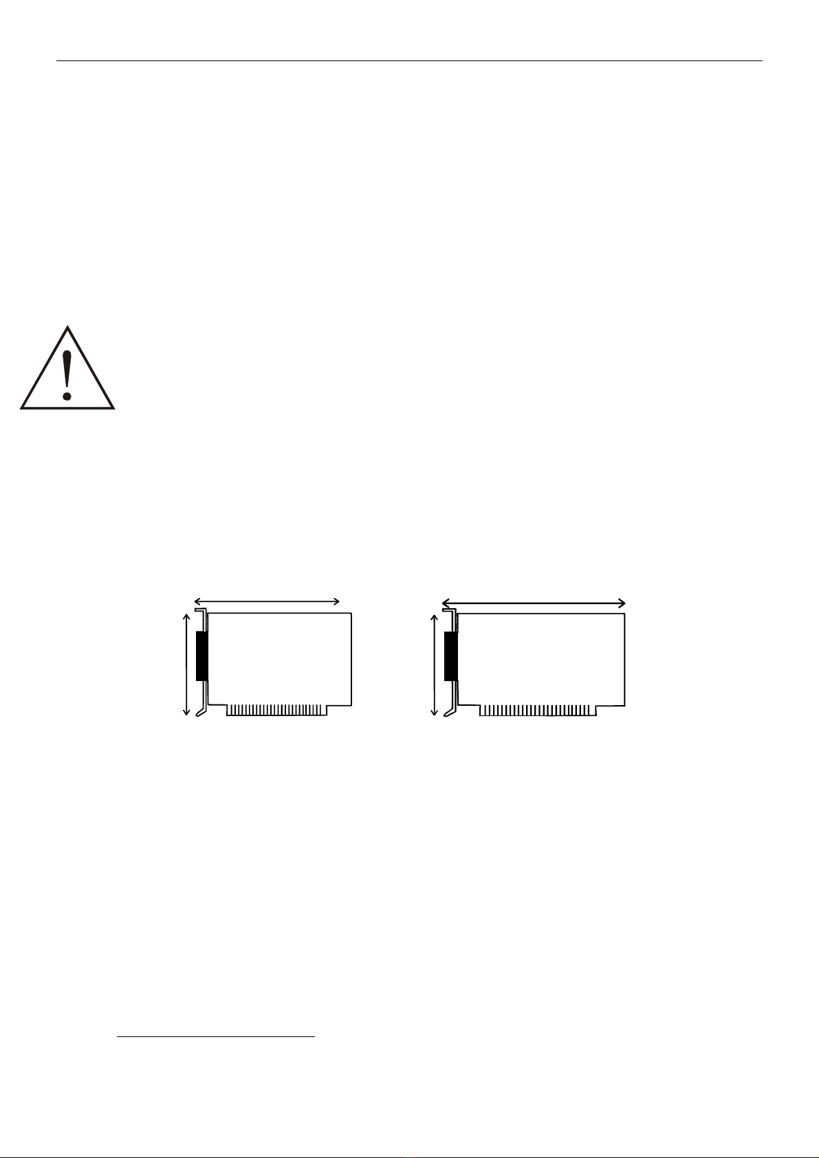
4.2 Physical set-up of the board
The board is assembled on a 4-layer printed circuit card.
Dimensions:
APCI-1032, APCI-2032
(PCI short board) APCI-1564
130 mm
99 mm
171 mm
99 mm
Weight: ..................................................... approx. 160 g
Installation in: ........................................... 32/64-bit PCI slot 5 V
Connection to the peripheral: ................... 37-pin SUB-D male connector
Accessories2:
Standard cables: ........................................ ST010, ST011, ST022
Screw terminal panel: ............................... PX901-D,
PX901-DG,
PX901-ZG
or PX9000
Relay output board: .................................. PX8500
ACPI-1564: ribbon cable FB1564 for the digital inputs
1We can transmit you the configuration on request.
2Not included in the standard delivery.

APCI-1032, APCI-1564 and APCI-2032 Technical data
15
WARNING!
The supply lines must be installed safely against mechanical
loads.
4.3 Versions
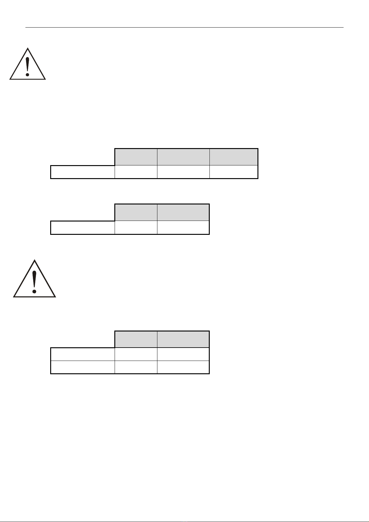
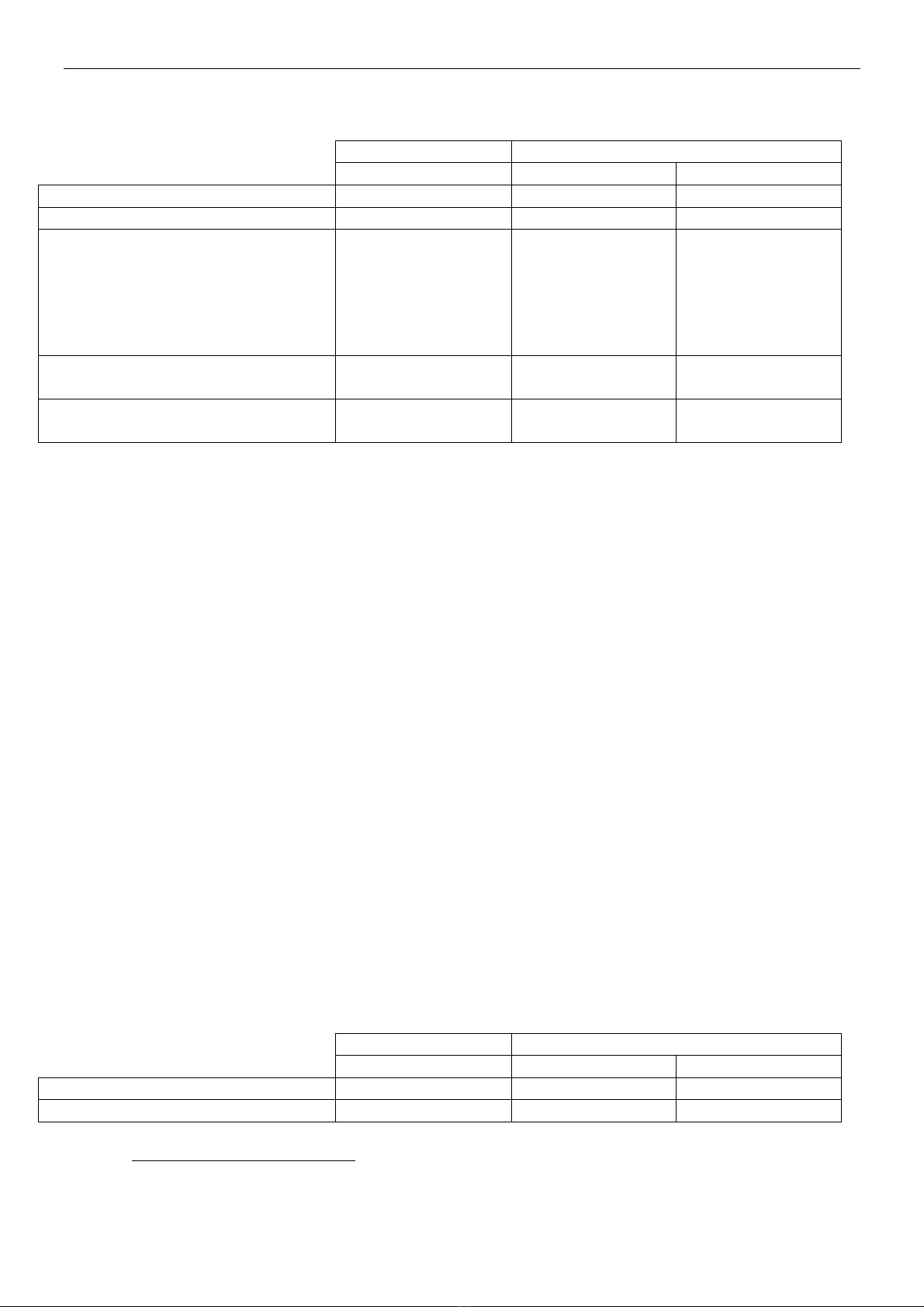
The boards are available in the following versions:
APCI-1032: 32 digital inputs
APCI-1032 APCI-1032-12 APCI-1032-5
Input voltage 24 V 12 V on request 5 V on request
APCI-2032: 32 digital outputs
APCI-2032 APCI-2032-5
Output voltage 24 V 5 V on request
APCI-1564: 32 digital inputs and 32 digital outputs
WARNING for the APCI-1564!
When all inputs are connected, the temperature of the printed
circuit card increases.
Make sure that the maximum supply voltage of 26 V is not exceeded. Please
consider the given Limit values. (See below)
APCI-1564 APCI-1564-5
Input voltage 24 V 5 V on request
Output voltage 24 V 5 V on request
4.4 Limit values
Max. altitude: ............................................ 2000 m
Operating temperature: ............................. 0 to 60°C
Storage temperature: ................................. -25 to 70°C
Relative humidity at indoor installation
50% at +40 °C
80% at +31 °C
Minimum PC requirements:
PCI BIOS from Version 1.0

APCI-1032, APCI-1564 and APCI-2032 Technical data
16
Bus speed: ................................................. < 33 MHz
Operating system: ..................................... Windows NT, 98, 2000, XP
Energy requirements:
APCI-1032
- Operating voltage of the PC: .................. 5 V ±5%
- Current consumption (without load): ..... 180 mA ±10 mA
APCI-2032
External operating voltage:
APCI-2032: ............................................... 24 V ±5%
APCI-2032-5: ........................................... 5 V-12 V ±5%
Max. current consumption1 (+ 5 V from PC):
APCI-2032: ............................................... 224 mA ±10%
APCI-2032-5 ............................................ 222 mA ±10%
APCI-1564
External operating voltage:
APCI-1564: ............................................... 24 V ±5%
APCI-1564-5: ........................................... 5 V-12 V ±5%
Max. current consumption3
(+ 5 V from PC):........................................ 380 mA ±10 %
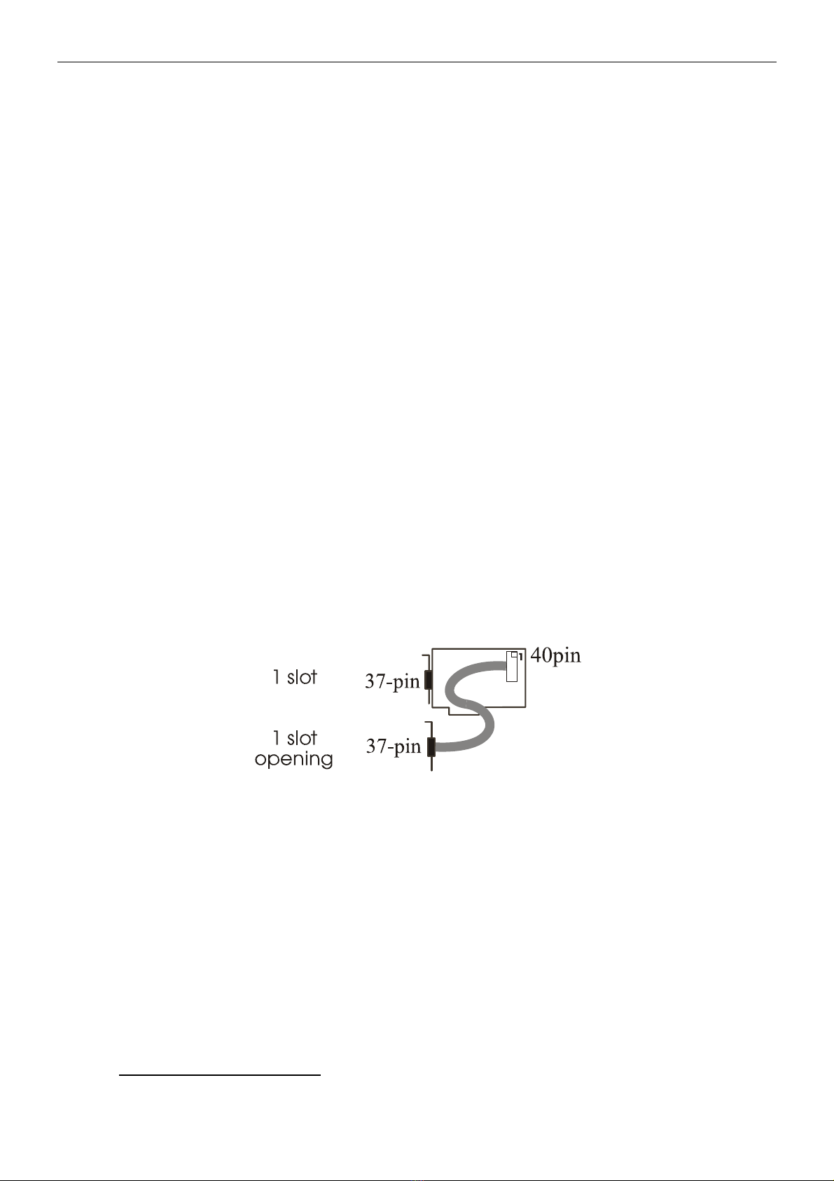
Number of slot required:
APCI-1032, APCI-2032: .......................... 1
APCI-1564: ............................................... 1+1
4.4.1 Digital inputs
24 V digital input channels
Input type: ................................................. mass related inputs
Number of input channels: ....................... 32
Nominal voltage: ...................................... 24 VDC
3All inputs and/or outputs are connected.

APCI-1032, APCI-1564 and APCI-2032 Technical data
17
APCI-1032 APCI-1564
32 (Channels 0 to 31) Channels 0 to 3 Channels 4 to 31
Interruptible inputs 16 (Channels 0 to 15) - 16 (channels 4 to 19)
Input current at nominal voltage 5 mA 10,5 mA 5 mA
Logic input level (Standard)
UH4max.:
UH min.:
UL5max.:
ULmin.:
30 V / 7.3 mA typ.
19 V / 3.2 mA typ.
14 V / 1.3 mA typ.
0 V
26 V / 12.3 mA typ.
19 V / 5.5 mA typ.
14 V / 0.7 mA typ.
0 V
26 V / 5 mA typ.
19 V / 3.2 mA typ.
14 V / 1.3 mA typ.
0 V
Signal delay
(at nominal voltage)
70 μs 1 μs 70 μs
Maximum input frequency
(at nominal voltage)
5 kHz 500 kHz 5 kHz
12 V digital input channels (APCI-1032)
Input type: ................................................. mass related inputs
Number of input channels: ....................... 32
Interruptible inputs: .................................. 16 (input 0 to 15)
Nominal voltage: ...................................... 12 VDC
Input current at nominal voltage: .............. 6 mA
Logic input level: ...................................... UH max.: 16 V / 9 mA typ.
UH min.: 8 V / 2 mA typ.
UL max.: 6 V / 0.7 mA typ.
ULmin.: 0 V
Signal delay: ............................................. 70 μs (at nominal voltage)
Maximum input frequency: ...................... 5 kHz (at nominal voltage)
5 V digital input channels
Input type: ................................................. mass related inputs
Number of input channels: ....................... 32
Nominal voltage: ...................................... 5 VDC
APCI-1032 APCI-1564
32 (channels 0 to 31) Channels 0 to 3 Channels 4 to 31
Interruptible inputs 16 (channels 0 to 15) - 16 (channels 4 to 19)
Input current at nominal voltage 6 mA 8.5 mA 6 mA
4 UH: Eingangsspannung, logisch "1"
5UL: Eingangsspannung, logisch "0"

APCI-1032, APCI-1564 and APCI-2032 Technical data
18
Logic input level (Standard)
UH6max.:
UH min.:
UL7max.:
ULmin.:
6 V / 8.4 mA typ.
4V / 4 mA typ.
2 V / 0.7 mA typ.
0 V
6 V / 11.3 mA typ.
4 V / 5.5 mA typ.
2 V / 1 mA typ.
0 V
6 V / 8.4 mA typ.
4 V / 4 mA typ.
2 V / 0.8 mA typ.
0 V
Signal delay
(at nominal voltage)
70 μs 1 μs 70 μs
Maximum input frequency
(at nominal voltage)
5 kHz 500 kHz 5 kHz
Safety (all boards)
Optical isolation
(DIN VDE 0411-100): .............................. 1000 V (from the PC to the
external peripheral).
4.4.2 Digital outputs
Switching times of the outputs - complies with norm IEC 1131
3 switching times are defined for the outputs.
Fig. 4-1: Switching times of the digital outputs
Output delay time: tdon or tdoff
Output transfer time for transition 0 Æ1: Rising time (tr)
Output transfer time for transition 1 Æ0: Falling time (tf)
24 V digital output channels
Output type: .............................................. high side (load at ground)
Number of output channels: ..................... 32
Nominal voltage: ...................................... 24 VDC
Range of the supply voltage: .................... 10 V to 36 VDC
(over 24 V ext. pins)
Max. output current
for outputs 0-15: ........................................ 3 A typ. (fused through
PTC resistors)
6 UH: Eingangsspannung, logisch "1"
7UL: Eingangsspannung, logisch "0"

APCI-1032, APCI-1564 and APCI-2032 Technical data
19
for outputs 16-31: ...................................... 3 A typ. (fused through
PTC resistors)
Max. output current / output channel: ...... 500 mA
Short-circuit current / output channel at 24 V,
Rload < 0.1 Ω: .......................................... 1.5 A max.: switches off the
component (4 channels)
ON-resistor of the output channel
(RDS ON resistor): .................................... 0.4 Ωmax.
Overtemperature: ......................................
ϑ
IC > 170°C: switches off the
component (4 channels)
Temperature hysteresis: ............................ 20°C
Switching time of the 24 V outputs
Rising time (tr): ......................................... typ. 94 µs, max. 250 μs
Falling time (tf): ........................................ typ. 8 µs, max. 20 μs
Output delay times
Switch ON time: ....................................... typ. 52 µs, max. 150 µs +
delay time of the opto-couplers
Switch OFF time: ..................................... typ. 80 µs, max. 150 µs +
delay time of the opto-couplers
Interruptible diagnostics, read back through status bit
ϑ
-diagnostic: ............................................ Pin 19 (24V/10 mA) is switched
on in case of overload of the
outputs or overtemperature
Vcc-diagnostic: .......................................... is switched on in case of voltage
drop < 5 V
Safety (24 V outputs)
Optical isolation
(DIN VDE 0411-100): .............................. 1000 V (from the PC to the
external peripheral).
Watchdog: ................................................. 8-bit watchdog.
programmable times from 20 ms
to 5 s in steps of 20 ms are
available.
5 V digital output channels
Output type: .............................................. open collector
Number of output channels: ..................... 32
Nominal voltage: ...................................... 5 VDC
Range of the supply voltage: .................... 5 V to 12 VDC
(over 5 V ext. pins)
Max. output current
per output component (8 channels): ......... 400 mA typ. (fused through
PTC resistors)
Max. output current / output channel: ...... 50 mA
Short-circuit current / output channel at 5 V,
Rload < 0.1 Ω: .......................................... Æ400 mA: limited through PTC

APCI-1032, APCI-1564 and APCI-2032 Technical data
20
Switching time of the 5 V outputs
Rising time (tr): ......................................... typ. 280 ns, max. 560 ns
Falling time (tf): ........................................ typ. 100 ns, max. 200 ns
Output delay times
Switch ON time: ....................................... typ. 18 µs, max. 100 µs +
delay time of the opto-couplers
Switch OFF time: ..................................... typ. 1.5 µs, max. 150 µs +
delay time of the opto-couplers
External Vcc < 3 V: ................................... Vcc-diagnostic is interruptible,
can be read back through status bit
Safety (5 V outputs)
Optical isolation
(DIN VDE 0411-100): .............................. 1000 V (from the PC to the
external peripheral).
Watchdog: ................................................. 8-bit watchdog.
programmable times from 20 ms
to 5 s in steps of 20 ms are
available.
5 V digital outputs type UDN2982
Output type: .............................................. High Side
Number of outputs: ................................... 32
Nominal voltage: ....................................... 24 VDC
Range of supply voltage: .......................... 5 V to 35 VDC
(over 24 V ext. pins)
Max. output current (in mA typ.):
per output driver (8 channels): .................. 400 mA (fused through PTC).
Max. output current: ................................. 50 mA
Short circuit current/output at 24 V,
Rlast < 0,1 Ω: ........................................... Æ400 mA
(limited through PTC)
Switch ON time UDN2982 (tr): ................ typ. 1 μs, max. 2 μs
Switch OFF time UDN2982 (tf): ............. typ. 5 μs,, max. 10 μs,
Switch delay signal chain optocoupler and driver UDN2982
at switching on: ......................................... typ. 18 µs, max. 100 µs +
(optocoupler delay)
at switching off: ........................................ typ. 27 µs, max. 150 µs
(optocoupler delay)
External Vcc < 3 V: ................................... Vcc-diagnosis is interruptible
Rereadable status bit
Short circuit:
Over the PTC all channels are switched off when thermal overload of the component.
Timer, interruptible (only for APCI-1564)
Number: .................................................... 1
Timer depth: ............................................. 12-bit
Time unit: ................................................. µs, ms, s
Counter, interruptible (only for APCI-1564)
Number: .................................................... 3
This manual suits for next models
2
Table of contents
Other Addi-Data PCI Card manuals

Addi-Data
Addi-Data ADDICOM APCI-7501 Parts list manual

Addi-Data
Addi-Data APCI-1710 User manual

Addi-Data
Addi-Data APCI-3701 Parts list manual

Addi-Data
Addi-Data APCIe-1711 Parts list manual

Addi-Data
Addi-Data APCI-3003 Parts list manual

Addi-Data
Addi-Data PC104-PLUS1500 Parts list manual

Addi-Data
Addi-Data ADDICOM APCI-7300 Parts list manual

Addi-Data
Addi-Data APCIe-1711 Parts list manual

Addi-Data
Addi-Data APCIe-040 Parts list manual