List of Figures
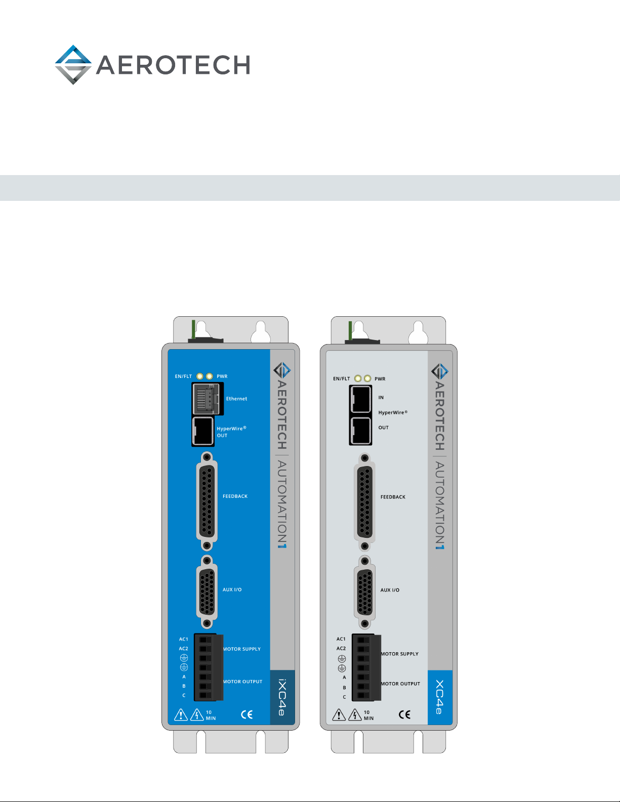
Figure 1-1: iXC4e Digital Drive-Based Controller 17
Figure 1-2: XC4e Digital Drive 18
Figure 1-3: Functional Diagram 20
Figure 1-4: Dimensions 24
Figure 1-5: Dimensions [-EB1] 25
Figure 2-1: Control Supply Connections 27
Figure 2-2: Motor Supply Connections 28
Figure 2-3: TV0.3-28-56-ST Transformer Control and Motor Power Wiring (40 VDC Bus) 30
Figure 2-4: TV0.3-28-56-ST Transformer Control and Motor Power Wiring (80 VDC Bus) 31
Figure 2-5: TV0.3-28-56-ST Transformer Control and Motor Power Wiring (160 VDC Bus) 32
Figure 2-6: TV0.3-28 Transformer Control and Motor Power Wiring (40 VDC Bus) 33
Figure 2-7: TV0.3-56 Transformer Control and Motor Power Wiring (80 VDC Bus) 34
Figure 2-8: TM3/TM5 Transformer Control and Motor Power Wiring 35
Figure 2-9: Brushless Motor Configuration 38
Figure 2-10: Positive Motor Direction 39
Figure 2-11: Encoder and Hall Signal Diagnostics 39
Figure 2-12: Brushless Motor Phasing Oscilloscope Example 40
Figure 2-13: Brushless Motor Phasing Goal 40
Figure 2-14: DC Brush Motor Configuration 41
Figure 2-15: Positive Motor Direction 41
Figure 2-16: Stepper Motor Configuration 42
Figure 2-17: Positive Motor Direction 42
Figure 2-18: Three Phase Stepper Motor Configuration 43
Figure 2-19: Positive Motor Direction 43
Figure 2-20: Square Wave Encoder Schematic (Feedback Connector) 46
Figure 2-21: Absolute Encoder Schematic (Feedback Connector) 47
Figure 2-22: Sine Wave Encoder Phasing Reference Diagram 48
Figure 2-23: Sine Wave Encoder Schematic (Feedback Connector) 49
Figure 2-24: Encoder Phasing Reference Diagram (Standard) 50
Figure 2-25: Position Feedback in the DiagnosticDisplay 50
Figure 2-26: Hall-Effect Inputs Schematic (Feedback Connector) 51
Figure 2-27: Thermistor Input Schematic (Feedback Connector) 52
Figure 2-28: Encoder Fault Input Schematic (Feedback Connector) 53
Figure 2-29: End of Travel and Home Limit Input Connections 55
Figure 2-30: End of Travel and Home Limit Input Schematic (Feedback Connector) 55
Figure 2-31: End of Travel and Home Limit Input Diagnostic Display 56
Figure 2-32: Brake Connected to the 25-Pin Feedback Connector (Typical) 57
Figure 2-33: Typical STO Configuration 59
Figure 2-34: STO Timing 63
Figure 2-35: Square Wave Encoder Interface (Aux I/OConnector) 66
Figure 2-36: Absolute Encoder Schematic (Auxiliary I/O Connector) 67
Figure 2-37: Sine Wave Encoder Phasing Reference Diagram 68
Figure 2-38: Sine Wave Encoder Schematic (Auxiliary I/OConnector) 69
Figure 2-39: PSO Interface 71
Figure 2-40: Digital Output Schematic (Aux I/OConnector) 73
Figure 2-41: Digital Outputs Connected in Current Sourcing Mode 74
Figure 2-42: Digital Outputs Connected in Current Sinking Mode 74
Figure 2-43: Digital Inputs Schematic (Aux I/OConnector) 75
Hardware Manual iXC4e/XC4e
www.aerotech.com 5